
 Open Access Article
 This Open Access Article is licensed under a Creative Commons Attribution-Non Commercial 3.0 Unported Licence
Photoluminescence through in-gap states in phenylacetylene functionalized silicon nanocrystals†
Arzu
Angı
a,
Regina
Sinelnikov
b,
Al
Meldrum
c,
Jonathan G. C.
Veinot
b,
Isacc
Balberg
d,
Doron
Azulay
d,
Oded
Millo
*d and
Bernhard
Rieger
*a
aWACKER-Lehrstuhl für Makromolekulare Chemie, Technische Universität München, Lichtenbergstrasse 4, 85747 Garching, Germany. E-mail: rieger@tum.de
bDepartment of Chemistry, University of Alberta, 11227 Saskatchewan Drive, Edmonton, Alberta, Canada T6G 2G2
cDepartment of Physics, University of Alberta, Edmonton, Alberta T6G 2G2, Canada
dRacah Institute of Physics, The Hebrew University of Jerusalem, Jerusalem 91904, Israel. E-mail: milode@mail.huji.ac.il
First published on 17th March 2016
Abstract
Optoelectronic properties of Si nanocrystals (SiNCs) were studied by combining scanning tunneling spectroscopy (STS) and optical measurements. The photoluminescence (PL) of phenylacetylene functionalized SiNCs red shifts relative to hexyl- and phenyl-capped counterparts, whereas the absorption spectra and the band gaps extracted from STS are similar for all surface groups. However, an in-gap state near the conduction band edge was detected by STS only for the phenylacetylene terminated SiNCs, which can account for the PL shift via relaxation across this state.
Silicon nanocrystals (SiNCs) have gained significant interest in recent years due to their intriguing properties that are not exhibited by their bulk counterparts. When the dimensions of SiNCs are reduced below the Bohr radius of an exciton in Si (∼4.5 nm),1 they photolumience at energies that are tunable by defining the SiNC size2–4 and surface functionalization.5–8 This, in combination with their low toxicity,9 biocompatibility10 and elemental abundance of Si, makes SiNCs a promising material for several applications including LEDs,11 solar cells,12 sensors13 and photoluminescent biomarkers.10
The surface chemistry of SiNCs can have a significant impact on their optoelectronic properties.5 For instance, SiNC photoluminescence has been tuned across the visible spectrum by changing surface groups (i.e., amine, phosphine, oxide and acetal) without altering the NC size.14 In this context, controlling surface characteristics via surface functionalization is essential to make SiNCs useful in optoelectronic applications by preserving and/or controlling their properties.
Recently, we presented the surface functionalization of hydride terminated SiNCs with organolithium reagents.15 This method offers, for the first time, the opportunity to bind aryl and alkynyl groups, such as phenyl and phenylacetylene, directly to the hydride terminated SiNC surface while ensuring monolayer coverage. Subsequent to the functionalization, we observed that SiNC PL was influenced by the surface group identity. For phenylacetylene functionalized SiNCs, the PL maximum red-shifted to ∼735 nm, compared to hexyl and phenyl functionalized SiNCs which emitted at ∼685 nm (Fig. 1).15,16 Elucidating the mechanism leading to this phenomenon is of great interest because it may provide insights into the influence of conjugated surface groups on SiNC electronic structures and optoelectronic properties.
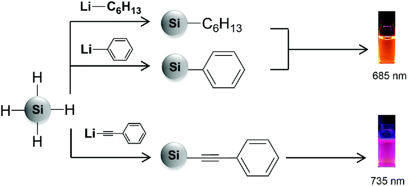 | ||
| Fig. 1 Influence of hexyl, phenyl and phenylacetylene groups on PL emission of SiNCs. | ||
In this work, we present a detailed analysis of the optoelectronic properties of hexyl, phenyl and phenylacetylene functionalized SiNCs with an attempt to explain the PL red-shift observed with phenylacetylene surface groups by utilizing PL and UV-Vis spectroscopy, excited state lifetime measurements and scanning tunneling microscopy/spectroscopy (STM/STS). STS results show that the band gap of the SiNCs is nearly independent of these three surface groups studied. However, for SiNCs functionalized with phenylacetylene, the tunneling spectra reveal the formation of an in-gap state close to the conduction band edge of SiNCs. The PL shift to a lower energy can be attributed to a transition via this in-gap state, which reduces the apparent band gap for recombination. To the best of our knowledge, this is the first time that an in-gap state, intentionally introduced via surface functionalization, has been observed by STS for SiNCs.
The SiNCs used in this work were synthesized by thermolysis of hydrogen silsesquioxane (HSQ) at 1100 °C for 1 hour under an atmosphere consisting of 5% hydrogen and 95% nitrogen.17 This procedure yields SiNCs in a silica-like matrix. Freestanding, hydride terminated SiNCs are obtained by etching the composite with ethanolic HF and final extraction into toluene.
Surface functionalization was performed by dispersing SiNCs, freshly etched from a 300 mg Si/SiO2 composite, in 2 mL 0.1 M solution of the organolithium reagent in toluene and stirring overnight at room temperature. The reaction was quenched upon addition of an acidified methanol–ethanol mixture, and the functionalized SiNCs were further purified by two antisolvent precipitation–dispersion steps.
FT-IR spectroscopy was utilized to confirm the surface functionalization. The freshly etched, hydride terminated SiNCs showed only Si–H bands in the IR spectrum at 2100, 906, and 660 cm−1, without any indication of oxidation (Fig. 2A). For the SiNCs functionalized with n–hexyllithium, strong C–H and C–C stretching bands appeared at ca. 2900 and 1450 cm−1, respectively (Fig. 2B). In the case of phenyl and phenylacetylene functionalized SiNCs, the IR spectra displayed aromatic C−H stretching modes between 3020 and 3085 cm−1 and aromatic C–C stretching peaks at 1595, 1490 and 1442 cm−1, together with aromatic overtones between 1600 and 2000 cm−1 (Fig. 2C and D). For phenylacetylene functionalized SiNCs, an asymmetric C![[triple bond, length as m-dash]](https://www.rsc.org/images/entities/char_e002.gif) C alkyne stretching band was observed at 2150 cm−1 as a shoulder on Si–H stretching at 2100 cm−1. In every case, only a minor surface oxidation was observed, evidenced by the Si–O band at 1050 cm−1.
C alkyne stretching band was observed at 2150 cm−1 as a shoulder on Si–H stretching at 2100 cm−1. In every case, only a minor surface oxidation was observed, evidenced by the Si–O band at 1050 cm−1.
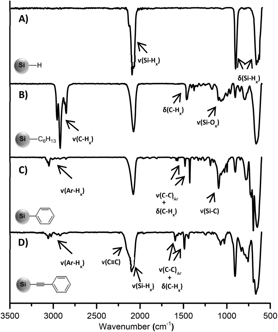 | ||
| Fig. 2 FT-IR spectra of (A) hydride terminated SiNCs; SiNCs functionalized with (B) n–hexyllithium; (C) phenyllithium; (D) lithium phenylacetylide. | ||
The PL spectra show that both hexyl and phenyl functionalized SiNCs emit at around 685 nm. However, when the SiNCs are functionalized with phenylacetylene, the PL maximum red-shifts to 735 nm, (Fig. 3) despite the particle size remaining constant.
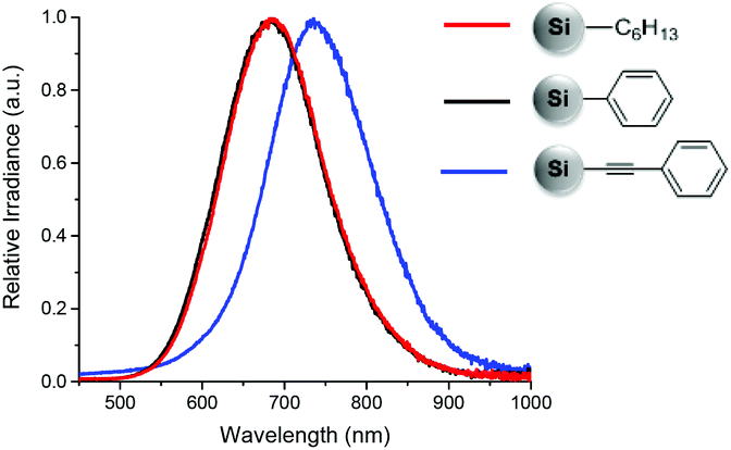 | ||
| Fig. 3 PL spectra of SiNCs functionalized with n-hexyllithium (red), phenyllithium (black) and lithium phenylacetylide (blue). | ||
The influence of surface-bonded molecules on the optical properties of SiNCs is a complex issue. Surface groups can modify the optical transitions of NCs by introducing additional surface states and defects.14,18 In general, size dependent, red/NIR PL emission accompanied by an excited life-time in the range of microseconds, dominantly originates from quantum confined band gap emission.19 In our study, observed PL decay curves (ESI Fig. S1†) were strongly non-exponential. The decay traces were fit with a log–normal lifetime distribution,20 which is applicable for ensembles of SiNCs.21 From the fitting parameters, we extracted a mean lifetime of 89.6, 79.7, and 102.1 μs for the hexyl, phenyl and phenylacetylene functionalized SiNCs, respectively. Since red PL, together with μs excited-state lifetime was observed, the PL is considered to be through a band gap transition.7,19
In several reports, shifts in PL emission maxima of SiNCs induced by different surface groups were observed together with changes in UV-Vis absorption.6,18 In the present work, even though the PL wavelength of phenylacetylene functionalized SiNCs appears at a lower energy, the absorption spectra obtained for hexyl, phenyl and phenylacetylene did not show any significant difference in the absorption edge (Fig. 4).
 | ||
| Fig. 4 UV-Vis spectra of SiNCs functionalized with n-hexyllithium (red), phenyllithium (black) and lithium phenylacetylide (blue). Absorption is normalized at 300 nm. | ||
This, as well as direct evaluation (TEM and STM) of the NC size (vide infra) rule out the possibility that the difference in PL spectra arises from an effective reduction of the SiNC diameter upon treatment with phenyllithium or hexyllithium reagents or to a different dielectric confinement effect22 in phenylacetylene functionalized SiNCs. If this was the case, these effects should contribute equally to the PL and absorption spectra leading to changes in both.
Difficulties associated with interpreting the optical spectroscopy data (PL and absorption) measured on SiNCs and relating them to the intrinsic level electronic structure are common.3,23,24 These challenges primarily stem from the fact that optical measurements alone cannot unambiguously determine the initial and final states associated with the excitation/recombination transitions. In particular, the influence of the surface groups on PL emission and the electronic structure of SiNCs cannot be deduced by optical spectroscopy. Clearly, complementary methods are required if the origin of the PL red-shift seen for the phenylacetylene functionalized SiNCs is to be elucidated.
STM/STS is one of the most effective tools for studying the electronic structure/properties of single colloidal semiconductor NCs.3,25 The main advantage of this approach over optical methods is STS provides information regarding the electronic density of states (DOS) by mapping the conduction band (CB) and valence band (VB) states independently. Therefore the single-particle (rather than excitonic) band gap can be evaluated directly.26 In addition, and most significant for our present work, the tunneling spectra can reveal in-gap states associated with either surface or NC-bulk defects.27,28 Such states are usually not observed in absorption measurements due to their very small absorption cross-sections.
STM images and a topographic cross-section taken on one of the isolated hexyl functionalized SiNCs, whose electronic structure was examined, are shown in Fig. 5A and B. All images were acquired with a set bias of 2.2 eV (well above the CB edge where the DOS of the SiNC is appreciable) and a set current of 0.2 nA. Under these conditions, the cross-section height corresponds well to the diameter of the SiNC, yielding in this case (and all other SiNCs presented here) a mean size of ∼3 nm. Further experimental details regarding the STM-STS measurements are given in the ESI.† TEM images of SiNCs functionalized with n–hexyllithium also reveal the average diameter of SiNCs around 3 nm (Fig. 5C). In the HR–TEM image, crystal lattice fringes are clearly seen (Fig. 5D).
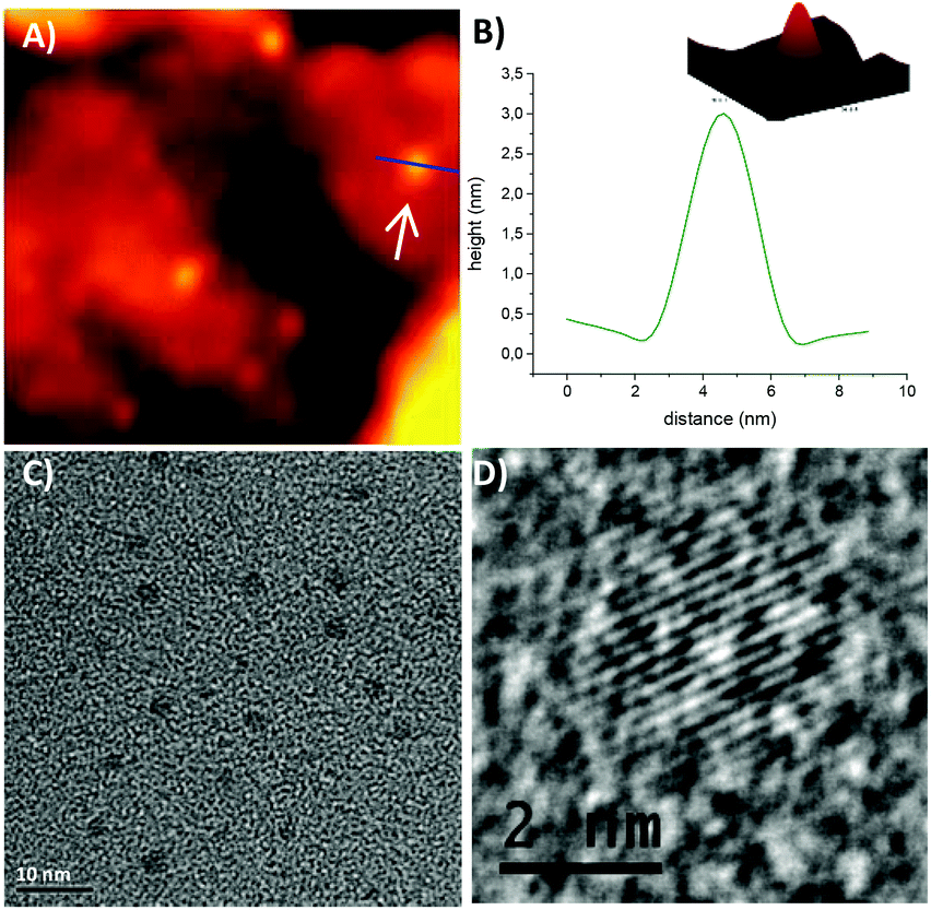 | ||
| Fig. 5 (A) STM image (150 × 150 nm2) showing isolated SiNCs functionalized with n-hexyllithium; (B) STM topographic image of a single SiNC marked by the white arrow in (A) and a cross-section taken along the blue line. (C) TEM image of n-hexyllithium functionalized Si-NCs with an average diameter of 3 nm; (D) HR-TEM image of 3 nm SiNCs functionalized with n-hexyllithium, lattice-fringes are clearly observable. Both methods verify a 3 nm average size of the SiNCs. | ||
Tunneling spectra measured on isolated SiNCs are shown for all three different surface functionalities together with the corresponding STM topography images and cross-sections in the insets (Fig. 6). Band gaps are deduced directly from the STS data from the energy difference between the VB and CB edges. For each band, the edge is defined here as the mid-value between the position of the first peak (or shoulder) and the onset of detectable DOS.29 This method affords band gaps of hexyl and phenyl functionalized SiNCs of 2.1 ± 0.1 eV. Note that the band gap values obtained by STS are larger than exciton band gaps determined by PL maxima (685 nm = 1.81 eV.) The reason for that is predominantly three-fold. First, the electron–hole Coulomb interaction that is incorporated in the optical (excitonic) gap does not play a role in the fundamental single-particle gap measured by STS.26,30 Second, the tunneling spectra are measured in the double-barrier tunnel junction configuration and thus the apparent gap is broadened due to the effect of voltage division between the two tunnel barriers involved; the tip–SiNC and the SiNC–substrate junctions.26 Third, the polarization energy associated with electron tunneling through the SiNC also contributed to the widening of the measured gap.31 We note that the STS-extracted gaps found here are somewhat larger than those reported in ref. 3. This may be due to the different ligands used here, which may affect the latter two factors.
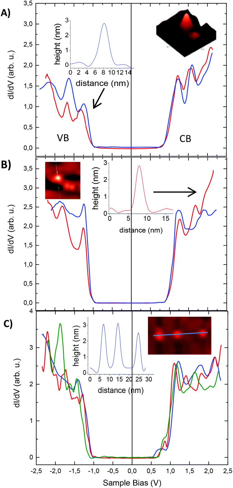 | ||
| Fig. 6 Tunneling spectra measured on ∼3 nm SiNCs functionalized with (A) n-hexyllithium; (B) phenyllithium; (C) lithium phenylacetylide. The insets show some of the NCs and the corresponding cross-section on which the spectra were acquired. The extracted band gaps of the Si-NCs are all around 2.1 eV, except for the green curve in (C) which was measured on the smaller, rightmost, NC. Importantly, the spectra measured on the phenylacetylene-capped SiNCs (in C) exhibit in-gap states close to the CB-edge. | ||
In the case of phenylacetylene functionalized SiNCs, the band gap is still in the range 2.1 ± 0.1 eV, in spite of the red-shifted PL. However, an in-gap state close to the CB-edge of the SiNCs is clearly observed in their tunneling spectra (Fig. 6C). This observation was very robust and detected in every measurement acquired for these NCs. The separation of the in-gap state from the CB-edge varied between 140 meV (red and green curves in Fig. 6C) and 190 meV (blue curve), where most spectra showed ∼160 meV separation. These values are in the range of, yet somewhat larger than, the PL red-shift (∼130 meV). The slight enlargement may be due to the aforementioned voltage division effect. After observing the in-gap state introduced by the phenylacetylene surface groups, along with the independence of the STS gap on surface functionalization, we suggest that the shift of PL to lower energy can be accounted for by a transition across this state, which reduces the apparent band gap for recombination.
Direct covalent bonding of a π-conjugated molecule to a silicon atom can efficiently reduce its HOMO–LUMO gap because of the σ*–π* conjugation between the Si core and the bonded conjugated molecule.32 The formation of states near band edges was theoretically expected to be the reason for the narrowing of the band gap.33 Such a conjugation between the Si core and the surface bound conjugated molecule can enhance the optical absorption of SiNCs at longer wavelengths which is highly desired for light harvesting applications. In contrast, no change in UV-Vis absorption was observed in the present system; this may result from the comparatively short conjugation length of phenylacetylene, and the corresponding small cross-section for photon absorption through these states. The effect of different conjugated surface groups with varied conjugation lengths on the optoelectronic properties and light harvesting efficiencies of SiNCs is under investigation.
Conclusions
In summary, we utilized STM/STS in combination with optical measurements to study the optoelectronic properties of hexyl, phenyl and phenylacetylene functionalized Si-NCs. PL emission of phenylacetylene functionalized SiNCs red-shifts for around 50 nm relative to hexyl- and phenyl-capped Si-NCs. No significant difference was observed in the band gaps deduced from STS and UV-Vis absorption measurements on Si-NCs terminated with these three different surface groups. However, for phenylacetylene functionalized SiNCs, the tunneling spectra revealed an in-gap state close to the CB edge. The lowering in PL emission energy can be attributed to a transition across this state, which reduces the apparent band gap for the recombination process. These results expand the understanding of the influence of the surface groups on the electronic structure of SiNCs and can lead to the control of the properties utilized in optoelectronic devices.Acknowledgements
B. R., J. G. C. V. and A. M. acknowledge the funding from DFG IRTG (2022) and NSERC CREATE programs for Alberta/TU München International Graduate School. J. G. C. V. and A. M. thank the NSERC DG program for continued generous support. A. A. is grateful for the scholarship from Studienstiftung des Deutschen Volkes. R. S. acknowledges the funding from AITF. O. M. and I. B. acknowledge support of the Harry de Jur Chair in Applied Science (O. M.), the Enrique Berman Chair in Solar Energy Research (I. B.) and the Focal Technology Area program within the Israel National Nanotechnology Initiative. Ignaz Höhlein is thanked for valuable discussions. Kai Cui is thanked for assistance with HR-TEM measurements.Notes and references
- E. G. Barbagiovanni, D. J. Lockwood, P. J. Simpson and L. V. Goncharova, J. Appl. Phys., 2012, 111, 34307 CrossRef.
- G. Ledoux, O. Guillois, D. Porterat, C. Reynaud, F. Huisken, B. Kohn and V. Paillard, Phys. Rev. B: Condens. Matter, 2000, 62, 15942–15951 CrossRef CAS.
- O. Wolf, M. Dasog, Z. Yang, I. Balberg, J. G. C. Veinot and O. Millo, Nano Lett., 2013, 13, 2516–2521 CrossRef CAS PubMed.
- X. Wen, P. Zhang, T. A. Smith, R. J. Anthony, U. R. Kortshagen, P. Yu, Y. Feng, S. Shrestha, G. Coniber and S. Huang, Sci. Rep., 2015, 5, 12469 CrossRef PubMed.
- K. Dohnalová, T. Gregorkiewicz and K. Kůsová, J. Phys.: Condens. Matter, 2014, 26, 173201 CrossRef PubMed.
- T. Zhou, R. T. Anderson, H. Li, J. Bell, Y. Yang, B. P. Gorman, S. Pylypenko, M. T. Lusk and A. Sellinger, Nano Lett., 2015, 15, 3657–3663 CrossRef CAS PubMed.
- M. Dasog and J. G. C. Veinot, Phys. Status Solidi B, 2014, 251, 2216–2220 CrossRef CAS.
- M. Dasog, J. Kehrle, B. Rieger and J. G. C. Veinot, Angew. Chem., Int. Ed., 2016, 55, 2322–2339 CrossRef CAS PubMed.
- J. Liu, F. Erogbogbo, K.-T. Yong, L. Ye, J. Liu, R. Hu, H. Chen, Y. Hu, Y. Yang, J. Yang, I. Roy, N. A. Karker, M. T. Swihart and P. N. Prasad, ACS Nano, 2013, 7, 7303–7310 CrossRef CAS PubMed.
- F. Erogbogbo, K.-T. Yong, I. Roy, G. Xu, P. N. Prasad and M. T. Swihart, ACS Nano, 2008, 2, 873–878 CrossRef CAS PubMed.
- F. Maier-Flaig, J. Rinck, M. Stephan, T. Bocksrocker, M. Bruns, C. Kübel, A. K. Powell, G. A. Ozin and U. Lemmer, Nano Lett., 2013, 13, 475–480 CrossRef CAS PubMed.
- M. Dutta, L. Thirugnanam, P. van Trinh and N. Fukata, ACS Nano, 2015, 9, 6891–6899 CrossRef CAS PubMed.
- C. M. Gonzalez, M. Iqbal, M. Dasog, D. G. Piercey, R. Lockwood, T. M. Klapötke and J. G. C. Veinot, Nanoscale, 2014, 6, 2608–2612 RSC.
- M. Dasog, G. B. De los Reyes, L. V. Titova, V. Lyubov, F. A. Hegmann and J. G. C. Veinot, ACS Nano, 2014, 8, 9636–9648 CrossRef CAS PubMed.
- I. M. D. Höhlein, A. Angı, R. Sinelnikov, J. G. C. Veinot and B. Rieger, Chem. – Eur. J., 2015, 21, 2755–2758 CrossRef PubMed.
- I. M. D. Höhlein, J. Kehrle, T. K. Purkait, J. G. C. Veinot and B. Rieger, Nanoscale, 2015, 7, 914–918 RSC.
- C. M. Hessel, E. J. Henderson and J. G. C. Veinot, Chem. Mater., 2006, 18, 6139–6146 CrossRef CAS.
- M. X. Dung, D. D. Tung, S. Jeong and H.-D. Jeong, Chem. – Asian J., 2013, 8, 653–664 CrossRef CAS PubMed.
- V. A. Belyakov, V. A. Burdov, R. Lockwood and A. Meldrum, Adv. Opt. Technol., 2008, 1–32 CrossRef.
- A. F. van Driel, I. S. Nikolaev, P. Vergeer, P. Lodahl, D. Vanmaekelbergh and W. L. Vos, Phys. Rev. B: Condens. Matter, 2007, 75, 35329 CrossRef.
- A. Nguyen, C. M. Gonzalez, R. Sinelnikov, W. Newman, S. Sun, R. Lockwood, J. G. C. Veinot and A. Meldrum, Nanotechnology, 2016, 27, 105501 CrossRef PubMed.
- T. Takagahara, Phys. Rev. B: Condens. Matter, 1993, 47, 4569–4584 CrossRef.
- M. Dasog, Z. Yang, S. Regli, T. M. Atkins, A. Faramus, M. P. Singh, E. Muthuswamy, S. M. Kauzlarich, R. D. Tilley and J. G. C. Veinot, ACS Nano, 2013, 7, 2676–2685 CrossRef CAS PubMed.
- M. V. Wolkin, J. Jorne, P. M. Fauchet, G. Allan and C. Delerue, Phys. Rev. Lett., 1999, 82, 197–200 CrossRef CAS.
- B. Marsen, M. Lonfat, P. Scheier and K. Sattler, Phys. Rev. B: Condens. Matter, 2000, 62, 6892–6895 CrossRef CAS.
- U. Banin and O. Millo, Annu. Rev. Phys. Chem., 2003, 54, 465–492 CrossRef CAS PubMed.
- D. Steiner, T. Mokari, U. Banin and O. Millo, Phys. Rev. Lett., 2005, 95, 56805 CrossRef CAS PubMed.
- Y. Bekenstein, K. Vinokurov, S. Keren-Zur, I. Hadar, Y. Schilt, U. Raviv, O. Millo and U. Banin, Nano Lett., 2014, 14, 1349–1353 CrossRef CAS PubMed.
- O. Millo, I. Balberg, D. Azulay, T. K. Purkait, A. K. Swarnakar, E. Rivard and J. G. C. Veinot, J. Phys. Chem. Lett., 2015, 6, 3396–3402 CrossRef CAS PubMed.
- A. Franceschetti and A. Zunger, Phys. Rev. B: Condens. Matter, 2000, 62, 2614–2623 CrossRef CAS.
- E. P. A. M. Bakkers, Z. Hens, A. Zunger, A. Franceschetti, L. P. Kouwenhoven, L. Gurevich and D. Vanmaekelbergh, Nano Lett., 2001, 1, 551–556 CrossRef CAS.
- J.-K. Choi, S. Jang, K.-J. Kim, H. Sohn and H.-D. Jeong, J. Am. Chem. Soc., 2011, 133, 7764–7785 CrossRef CAS PubMed.
- R. Wang, X. Pi and D. Yang, J. Phys. Chem. C, 2012, 116, 19434–19443 CAS.
Footnote |
| † Electronic supplementary information (ESI) available: Detailed experimental procedures, additional HR-TEM images and PL lifetime data. See DOI: 10.1039/c6nr01435f |
| This journal is © The Royal Society of Chemistry 2016 |