
 Open Access Article
 This Open Access Article is licensed under a
 Creative Commons Attribution 3.0 Unported Licence
Tunable top-down fabrication and functional surface coating of single-crystal titanium dioxide nanostructures and nanoparticles†
Seungkyu
Ha
,
Richard
Janissen
,
Yera Ye.
Ussembayev
,
Maarten M.
van Oene
,
Belen
Solano
and
Nynke H.
Dekker
*
Department of Bionanoscience, Kavli Institute of Nanoscience, Faculty of Applied Sciences, Delft University of Technology, Lorentzweg 1, 2628 CJ Delft, The Netherlands. E-mail: n.h.dekker@tudelft.nl
First published on 18th April 2016
Abstract
Titanium dioxide (TiO2) is a key component of diverse optical and electronic applications that exploit its exceptional material properties. In particular, the use of TiO2 in its single-crystalline phase can offer substantial advantages over its amorphous and polycrystalline phases for existing and yet-to-be-developed applications. However, the implementation of single-crystal TiO2 has been hampered by challenges in its fabrication and subsequent surface functionalization. Here, we introduce a novel top-down approach that allows for batch fabrication of uniform high-aspect-ratio single-crystal TiO2 nanostructures with targeted sidewall profiles. We complement our fabrication approach with a functionalization strategy that achieves dense, uniform, and area-selective coating with a variety of biomolecules. This allows us to fabricate single-crystal rutile TiO2 nanocylinders tethered with individual DNA molecules for use as force- and torque-transducers in an optical torque wrench. These developments provide the means for increased exploitation of the superior material properties of single-crystal TiO2 at the nanoscale.
Introduction
Micro- and nanostructures based on titanium dioxide (TiO2) have been utilized in numerous applications that exploit the unique properties of this material (Fig. S1†). For example, the high photocatalytic activity of TiO2 is used for water splitting1 and air purification.2 The electrical properties of TiO2, which include a tunable resistance, a high dielectric constant, carrier transport abilities, and a wide band gap, render it a preferred material for sensors,3 memory devices,4 transistors,5 solar cells,6 and batteries.7,8 Furthermore, the optical properties of TiO2, e.g. high refractive index and optical nonlinearity, make it find use in optical waveguides,9 photonic crystals,10 and optical trapping.11In particular, the use of TiO2 in its single-crystalline phase can offer substantial advantages over its amorphous and polycrystalline phases for existing and new applications. For instance, single-crystal TiO2 allows improved control of surface properties, e.g. photochemical reactivity12 and surface wettability,13 by making use of the different crystallographic orientations. The higher carrier mobility of single-crystal TiO2 renders it a promising material for transistors and (bio)sensors14 and may enhance the efficiency of dye-sensitized solar cells.15 Furthermore, optical waveguides and photonic crystals composed of single-crystal TiO2![[thin space (1/6-em)]](https://www.rsc.org/images/entities/char_2009.gif) 16,17 are expected, due to their highly ordered atomic structures, to exhibit improved light transmission and nonlinear responses.18,19 Lastly, the single-crystal rutile polymorph of TiO2 has an exceptionally large optical birefringence, which makes it an excellent candidate for incorporation into torque transducers for e.g. single-molecule spectroscopy.20
16,17 are expected, due to their highly ordered atomic structures, to exhibit improved light transmission and nonlinear responses.18,19 Lastly, the single-crystal rutile polymorph of TiO2 has an exceptionally large optical birefringence, which makes it an excellent candidate for incorporation into torque transducers for e.g. single-molecule spectroscopy.20
To facilitate the application of TiO2 in its single-crystalline phase, major challenges in both fabrication and surface functionalization must be addressed. First, it is important to control structural parameters such as feature size, shape, and pitch that determine the resulting physical responses of fabricated TiO2 nanostructures. Such physical responses impact e.g. gas sensing performance,3 light scattering efficiency,6 light propagation behavior,9 and optical trapping capabilities.11 Mainstream bottom-up approaches for TiO2 nanofabrication,21e.g. the hydrothermal growth method1,22 and electrochemical anodization,6 although capable of high throughput, lack sufficient flexibility in controlling dimensions and geometries. A number of bottom-up methods are capable of fabricating single-crystal TiO2 nanostructures, but these lack control of the crystallographic orientations and are limited to a certain crystalline polymorph, e.g. anatase23 or rutile.15 Hybrid fabrication methods, such as the atomic layer deposition array defined by etch-back technique,24,25 can achieve a high aspect-ratio but are limited to the fabrication of amorphous or polycrystalline TiO2.26 These limitations can be overcome by employing top-down nanofabrication methods based on plasma etching, which can target a single-crystal TiO2 substrate with any desired crystalline polymorph or crystallographic orientation. However, as TiO2 is substantially more difficult to etch than comparable materials (e.g., silicon (Si), silicon dioxide (SiO2), and silicon nitride (Si3N4)),27,28 such etching processes are currently limited to a low aspect-ratio and a largely positive sidewall angle.
Second, it is key to achieve highly efficient surface functionalization and bioconjugation of TiO2 for applications such as (bio)sensors,29 force transducers,30 and torque transducers.31 However, surface functionalization of TiO2, using common alkoxysilane surface linkers, is known to be less efficient in terms of linker density and uniformity than other oxide materials (e.g., SiO2 and aluminum oxide (Al2O3)).32,33 Furthermore, the majority of the described bioconjugation methods for TiO2 surfaces require a long incubation time and additional crosslinker molecules29 that could decrease the overall conjugation efficiency and harm the biomolecule functionality. Peculiarly for single-crystal TiO2 nanostructures, the lack of extensive quantitative and qualitative comparisons of different surface functionalization strategies hinders the selection of an optimal procedure.
Here, we present a successful top-down fabrication and surface functionalization of single-crystal TiO2 nanostructures and nanoparticles. We focus our efforts on the rutile polymorph of single-crystal TiO2 (100), in order to harness its exceptionally large optical birefringence and precisely oriented optic axis for effective torque transfer (ESI Methods†) in an optical torque wrench (OTW).20 Using high aspect-ratio nanocylinders suitable for optical trapping as our target structures, we demonstrate how these can be mass-produced with well-defined sizes and etch profiles that display excellent overall structural uniformity. We achieve a dense, uniform surface coating of TiO2 nanocylinders using different linker molecules, and we demonstrate subsequent covalent conjugation of biological and organic molecules such as DNA, streptavidin, biotin, and biocompatible poly(ethylene glycol) (PEG). We successfully exploit these developments to fabricate and functionalize TiO2 nanocylinders with single DNA molecules, and demonstrate full rotational control of individual nanocylinders in an OTW. This provides a particularly stringent test, as proper functioning of the OTW relies on both the correctly oriented optic axis and tightly controlled dimension of the single-crystal TiO2 nano-cylinder, and the quality and reliability of the surface coating. Rutile being the polymorph of TiO2 that is most difficult to etch,34 our approach provides the means for increased exploitation of the superior material properties of single-crystal TiO2 in any desired polymorph for diverse applications.
Results and discussion
Selecting an etch mask for the plasma etching of single-crystal TiO2
One of the major issues in top-down nanofabrication of single-crystal TiO2 is its high etch resistance. Plasma generated by fluorine-based gases is capable of etching TiO2 only under more aggressive etching conditions – in terms of plasma ion density and energy – than the ones employed for the dry etching of comparable materials e.g. Si, SiO2, and Si3N4. The increased difficulty in etching TiO2 compared to e.g. SiO2 stems from differences in the volatility of their etch byproducts: whereas SiFx is volatile, TiFx is not.27 The more aggressive physical etching conditions for TiO2 necessitate careful selection of the etch mask material: while a typical polymer-based mask (e.g., photoresist, electron beam (e-beam) resist, or polystyrene spheres) can provide sufficient etch selectivity (defined as the ratio of the substrate and mask etch rates) for e.g. SiO2,31 this is not the case for TiO2. The low etch selectivity imposes a thicker mask for a target etch depth, which is challenging as the applicable mask thickness is always limited (ESI Methods†). Also, masks can suffer from excessive edge erosion during etching, which in turn reduces both feature sizes and the ability to perform anisotropic etching.35To overcome these challenges, we have searched for a mask material for the dry etching of single-crystal TiO2 that achieves sufficiently high etch selectivity to permit the fabrication of nanostructures in a wide range of dimensions and sidewall profiles. We have compared different mask materials (Fig. S2†), such as chromium (Cr),36 tungsten (W), e-beam resist, and amorphous Si. We observe that in particular Cr provides a significantly higher etch selectivity in fluorine-based etching of rutile TiO2 (up to ∼28:1 under specific etching conditions; an overview of etch selectivity values for different etching conditions can be found in Fig. S3†) than the other tested materials. We therefore select Cr as an appropriate etch mask material. To fabricate the Cr mask, we create circular apertures in a poly(methyl methacrylate) (PMMA) layer using e-beam lithography (Fig. 1, steps 1–3). The aperture diameters can be tuned within 100–600 nm by means of defocusing e-beam. Subsequent Cr deposition and the following lift-off define the mask (Fig. 1, steps 4 and 5).
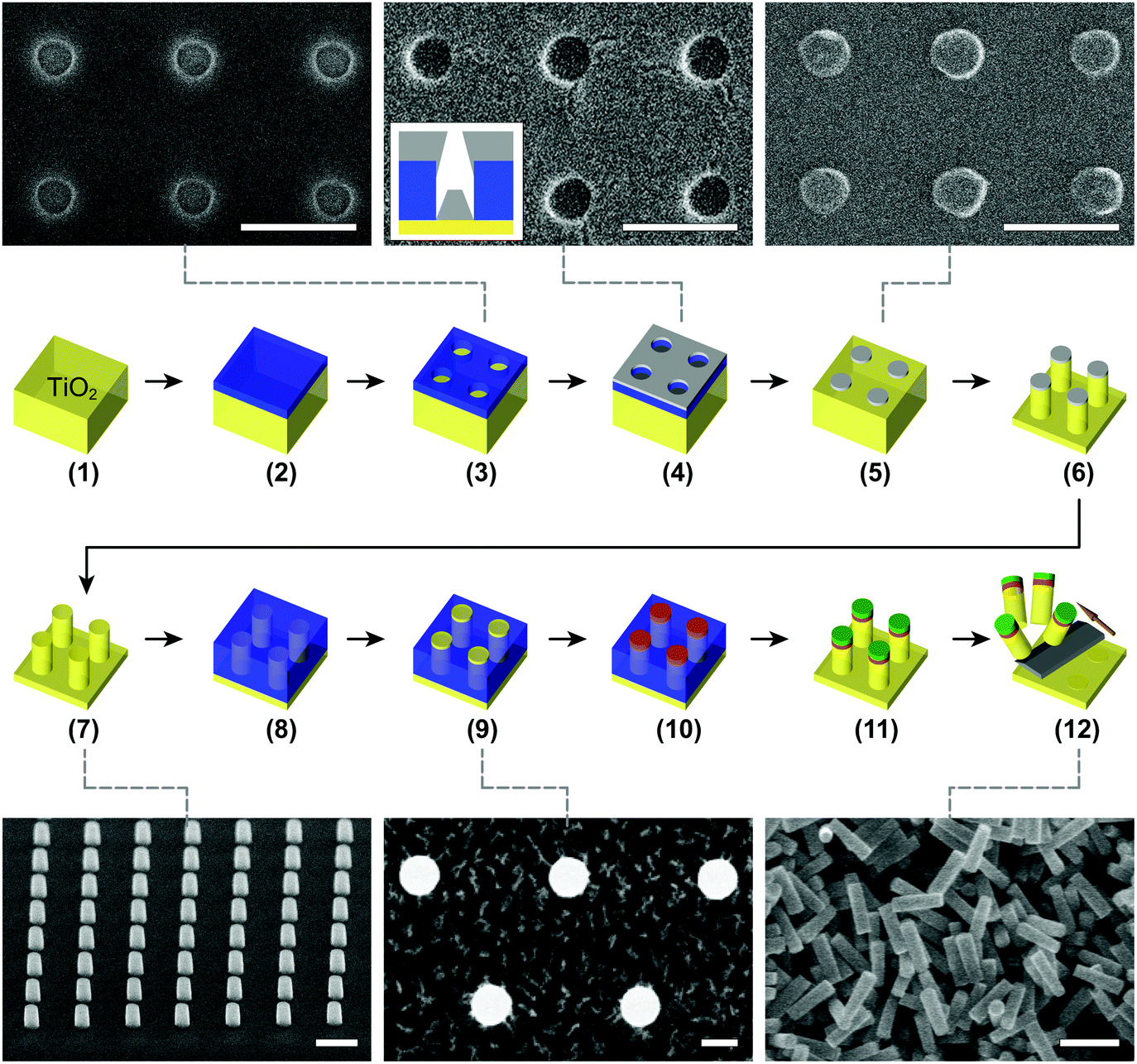 | ||
| Fig. 1 Schematic diagram of the fabrication protocol for single-crystal TiO2 nanostructures and nanoparticles. Each SEM image is linked to the corresponding step by a gray dashed line. Scale bars denote 500 nm. (Step 1) Cleaning of a single-crystal TiO2 substrate (yellow). (Step 2) PMMA (blue) spin-coating for e-beam lithography. (Step 3) E-beam patterning and subsequent development to generate evaporation windows that define the desired nanostructure sizes. The corresponding SEM image in the inset shows the TiO2 surfaces (circles) following exposure and development of the PMMA layer. (Step 4) Deposition of the Cr layer (light gray) through evaporation. The Cr layer covers both the accessible TiO2 surfaces (circles) and the PMMA layer (inset SEM image). The inset illustration shows a cross-section that highlights the formation of a Cr mask. (Step 5) Lift-off of the PMMA layer and the resulting Cr etch mask. The SEM image in the inset displays the Cr mask (circles) formed on the TiO2 substrate. (Step 6) Dry etching step to obtain the desired heights and sidewall profiles. (Step 7) Removal of the Cr mask following usage generates the complete nanostructures, and surface cleaning prepares these for subsequent surface functionalization. The SEM image (60° tilt) in the inset shows an array of the fabricated nanocylinders. (Step 8) Spin-coating of a temporary PMMA layer for area-selective functionalization. (Step 9) Etching of the temporary PMMA layer renders the tops of the nanostructures accessible. The SEM image in the inset shows the TiO2 nanostructures (white circles) amidst the etched PMMA layer. (Step 10) Selective surface functionalization with linker molecules (orange). (Step 11) Removal of the temporary PMMA layer and the following conjugation with biomolecules (green). (Step 12) Mechanical cleavage of the nanostructures using a microtome blade (dark gray) to generate isolated individual nanoparticles. The inset shows an SEM image of a batch of cleaved nanocylinders. For further details, see Methods. | ||
Trifluoromethane (CHF3)-based plasma etching of single-crystal TiO2 nanocylinders
With the objective to maximize the etch rate with a sufficiently high etch selectivity (>10:1, in order to achieve etch depths up to 1–2 μm at the practical upper limit of Cr mask thickness, ∼150 nm; ESI Methods†) and to produce single-crystal TiO2 nanocylinders with vertical sidewall angles, we have optimized parameters for the fluorine-based plasma etching process (Fig. 1, step 6). We start with a reactive ion etching (RIE) system in which trifluoromethane (CHF3) is the major etchant, and oxygen (O2) and argon (Ar) are additive gases. The major etchant gas CHF3 supplies both the reactive etching species and the fluorocarbon (CxFy) surface passivation layer-forming species.37 To optimize the process, we systematically vary the radio frequency (RF) power, chamber pressure, and ratios of the etch gases (CHF3:O2:Ar) (Table S1†). Our optimized etching conditions (Table S2†) result in a high single-crystal TiO2 etch rate of ∼40 nm min−1 at a sufficient etch selectivity of ∼14:1 over the Cr mask, which enables the formation of TiO2 nanocylinders with vertical sidewalls (∼90°; Fig. 2a). We have successfully implemented this protocol on a second, nominally identical RIE system (Fig. 2b), requiring only minor tuning in the O2 flow rate (4–8 sccm compared to ∼0.5 sccm), most likely due to differences in instrument calibration.
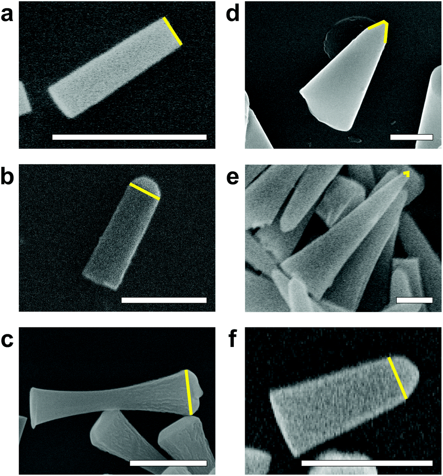 | ||
| Fig. 2 Control of single-crystal TiO2 nanocylinder shapes using different conditions in plasma etching. In each SEM image, the top surface of the nanocylinder is marked by a yellow line (remnants of the Cr mask prior to its removal are visible in (b, c and f)). Scale bars denote 500 nm. In the following, the height (H), the averaged diameter (D), and the resulting aspect-ratio (AR = H/D) of each nanocylinder are shown. (a) A nanocylinder with a vertical sidewall (89°) that results from an optimized CHF3:O2 dry etching in an RIE system (H: 430 nm, D: 110 nm, AR: 3.9). (b) A nanocylinder with a vertical sidewall (89°) etched from the optimized CHF3:O2 dry etching in a second, nominally identical RIE system (H: 605 nm, D: 205 nm, AR: 3.0). (c) An hourglass-shaped nanocylinder that results from CHF3:O2:Ar dry etching in an RIE system (H: 1020 nm, D: 200 nm, AR: 5.1). (d) A cone-shaped nanocylinder that results from SF6:CH4:Ar dry etching in an ICP-RIE system (H: 1385 nm, D: 490 nm, AR: 2.8). (e) A cone-shaped nanocylinder that results from SF6:He dry etching in an ICP-RIE system (H: 2160 nm, D: 390 nm, AR: 5.5). (f) A nearly vertical (85°) nanocylinder that results from an optimized SF6:He dry etching in an ICP-RIE system (H: 470 nm, D: 210 nm, AR: 2.2). | ||
Notably, we observe that tuning a single process parameter, namely the O2 flow rate, allows us to drastically alter sidewall etch profiles and even cross-sectional shapes (Fig. S3†). For example, at low O2 flow rates (0–1 sccm), we can modulate the sidewall angles from positive to negative, thereby including vertical sidewalls (Fig. 2a and b). At significantly higher O2 flow rates (5–10 sccm), we can obtain hourglass-shaped etch profiles (Fig. 2c).
Sulfur hexafluoride (SF6)-based plasma etching of single-crystal TiO2 nanocylinders
While maintaining identical objectives as above (high etch selectivity and vertical sidewall angles), we have also optimized the plasma etching of TiO2 using another major etchant, sulfur hexafluoride (SF6), in inductively coupled plasma (ICP)-RIE systems. We achieve higher etch rates of 100–200 nm min−1 (compared to those of 30–100 nm min−1 in RIE systems) using two different ICP-RIE systems (one equipped with SF6, methane (CH4), and Ar gases, Fig. 2d; the other equipped with SF6 and helium (He) gases, Fig. 2e and f), making it possible to fabricate TiO2 nanocylinders with heights up to 1–2 μm while reducing the time of exposure to the plasma. The latter is important because longer etch durations tend to induce a drift in the etching conditions which in turn leads to irregular etch profiles. The higher TiO2 etch rates that we obtain result from the increased density of plasma generated in ICP-RIE versus RIE systems28 and a reduced level of CxFy sidewall surface passivation. Decreased levels of CxFy passivation are attributed to an excess of hydrogen plasma38 and to the lack of a carbon source for the cases of SF6:CH4:Ar and SF6:He, respectively. Furthermore, SF6-etched nanocylinders show cleaner, smoother surfaces in high-resolution scanning electron microscopy (SEM) images (Fig. 2d) compared to those of CHF3-etched cylinders (Fig. 2c).
When we use non-optimized SF6-based plasma etching conditions, etch profiles displaying highly positive sidewall angles are obtained. Since the high plasma densities of ICP-RIE systems also significantly increase the Cr etch rates, we observe that the Cr mask tends to be completely etched away during the process, hence resulting in the formation of cone-shaped nanocylinders35 (Fig. 2d and e). Under our optimized etching conditions (Table S2†), which rely on a reduced ICP power to generate moderate plasma density, we are able to achieve sufficient etch selectivity over the Cr mask (∼16:1) and nearly vertical sidewall angles (∼85°; Fig. 2f) with high single-crystal TiO2 etch rates of ∼120 nm min−1.
Quantification of single-crystal TiO2 nanocylinder uniformity
To quantify both the local and global structural uniformity of fabricated single-crystal TiO2 nanocylinders over an entire substrate, we have analyzed SEM images of high aspect-ratio (3.6) nanocylinders fabricated using the CHF3 plasma-based protocol (Fig. 3; etching conditions in Table S2†). Qualitatively, the high uniformity of nanocylinder diameters and heights can be observed from the SEM image of a cleaved nanocylinder substrate (Fig. 3a). To quantify this, we measure the dimensions of nanocylinders at radial distances from the substrate center out to 3.5 mm and spaced by 0.5 mm (thus covering the entire circularly patterned area with a radius of ∼4 mm on the 10 × 10 mm2-sized substrate). From the analysis of top-view SEM images (Fig. 3b), we observe that the top (Fig. 3d) and bottom diameters (Fig. 3e) exhibit excellent local uniformity, defined as the uniformity at each measurement position (averaged relative standard deviation (RSD) of 4.4% (top) and 2.3% (bottom)). The global uniformity across the substrate displayed similar values (RSD of 4.7% (top) and 2.7% (bottom)). Fluctuations in diameters likely result from the instability of the e-beam during the patterning process of the Cr etch mask. The observation that the top diameters are nonetheless slightly less uniform than the bottom diameters may result from the fact that etching erodes the Cr mask in a non-uniform fashion depending on the roughness of the mask surface,39 as is backed up by an analysis of the roundness of the top and bottom nanocylinder surfaces (Fig. S4†). From tilted-view SEM images (Fig. 3c), we also extract the nanocylinder heights (Fig. 3f), which similarly show very good uniformity both locally (averaged RSD of 0.6%) and globally (RSD of 1.4%). We attribute the nearly monotonic increase in heights outward from the substrate center to the well-known loading effect, in which the transport and depletion of etching species along a substrate contribute to etch rate nonuniformity.40 The analysis of a batch of low aspect-ratio (1.6) nanocylinders reveals identical trends (Fig. S4 and Table S3;† etching conditions in Table S2†), thereby proving that our protocol can be used to generate both low and high aspect-ratio nanoscale structures with high uniformity.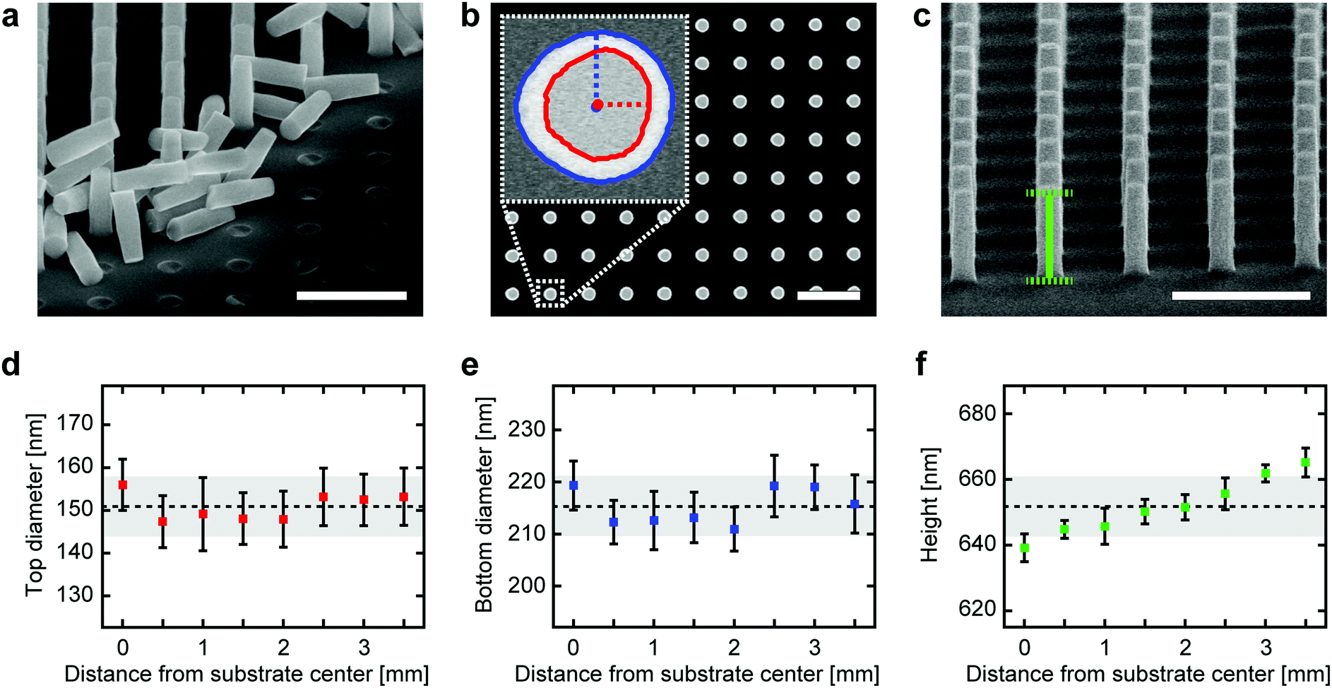 | ||
| Fig. 3 Dimensions of fabricated single-crystal TiO2 nanocylinders. (a–c) SEM images of etched TiO2 nanocylinders (light gray). Scale bars denote 1 μm. (a) Tilted-view (60°) of partially cleaved TiO2 nanocylinders. An array of rigidly fixed nanocylinders is visible in the top-left corner, and the cleaved substrate surface is in the bottom-right corner. The released nanocylinders are positioned at the interface of these regions. (b) Top-view of the nanocylinders. The inset shows the boundaries of the top (red contour line) and bottom (blue contour line) surface areas detected using the custom-written image analysis software routine. The dotted horizontal red (vertical blue) line and the red (blue) dot display the equivalent radius and the center of the top (bottom) surface, respectively. (c) Tilted-view (75°) together with an illustration of the image analysis procedure used to extract nanocylinder heights. The green vertical line measures the distance between the centers of the top and bottom surfaces (indicated by the green dotted horizontal lines). This distance is converted to the actual height using the tilting angle. (d–f) Quantification of nanocylinder diameters and heights over the substrate. Measurement points are spaced by 0.5 mm from the center of the substrate to its edge. At each point, the diameters (heights) are calculated from n = 12 (n = 10) different nanocylinders. The square markers and the error bars in the graphs represent the mean and the standard deviation of the local uniformity, respectively. The horizontal dotted black lines and the top and bottom sides of the gray shaded boxes in the graphs represent the mean and the standard deviation of the global uniformity, respectively. (d) Top diameters, (e) bottom diameters, and (f) heights are shown as a function of distance from the substrate center. | ||
Surface functionalization and bioconjugation of single-crystal TiO2
We now demonstrate highly efficient and versatile surface functionalization and bioconjugation of single-crystal rutile TiO2 (Fig. 4a). We perform the functionalization experiments on single-crystal TiO2 nanostructures fabricated using our developed SF6-based plasma etching process presented earlier. Compared with CHF3-based etching, this process results in a lower degree of surface contamination by CxFy, and hence a higher surface linker coverage.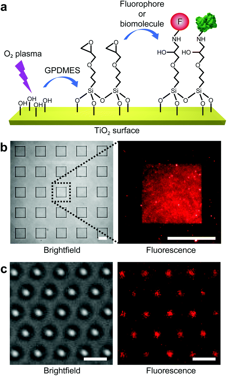 | ||
| Fig. 4 Characterization of the efficiency of surface functionalization of single-crystal TiO2 structures using fluorescence microscopy. (a) Illustration of the surface coating steps. First, single-crystal TiO2 surfaces are O2 plasma-treated to generate hydroxyl groups (–OH). Then epoxysilanes (GPDMES) are covalently bound to the surface hydroxyl groups. Consequently, either fluorophores (red) or biomolecules (e.g., streptavidin (green)) are bound covalently to the reactive epoxy functional group. (b) Functionalized micro-patterns for the quantitative characterization of the efficiency of surface functionalization. The brightfield image (left panel) shows squares (25 × 25 μm2) patterned on the PMMA-coated TiO2 substrate. The corresponding zoom-in fluorescence image (right panel) of a square shows successful covalent binding of the amino-labeled fluorophores (ATTO 647N) to the epoxysilane functionalized surface. Scale bars denote 20 μm. (c) Functionalized nanostructures for the qualitative characterization of the efficiency of surface functionalization. Brightfield (left panel) and the corresponding fluorescence (right panel) images of top-area functionalized TiO2 nanocylinders using the same method as above. Scale bars denote 2 μm. | ||
To quantitatively characterize the surface coating efficiency of different covalently bound surface linkers, we first test functionalization on single-crystal rutile TiO2 substrates with large-scale square micro-patterns (25 × 25 μm2) embedded in a thick (1–2 μm) PMMA layer (Fig. 4b). Similarly to other oxide materials, the surface of TiO2 is populated by hydroxyl groups that allow it to be functionalized with different types of linker molecules, such as silanes and other organic molecules with a covalent hydroxyl-binding capacity.33,41 Here, we have tested four different surface linker molecules: an aminoalcohol (ethanolamine hydrochloride; ETA), an epoxysilane ((3-glycidoxypropyl)dimethylethoxysilane; GPDMES), a widely used alkoxysilane ((3-aminopropyl)dimethylethoxysilane; APDMES), and a cyclic azasilane (N-n-butyl-aza-2,2-dimethoxysilacyclopentane; BADMSCP). Additionally, since PEG coatings are widely used for surface passivation42 and as biocompatibility layers,43 we have also tested the covalent attachment of heterobifunctional PEG to ETA-coated surfaces (ESI Methods, Fig. S5†). To compare the coating efficiency of these different linkers, we covalently bind fluorophores (ATTO 647N; λexcitation = 640 nm, λemission = 669 nm) to the functionalized micro-patterns and measure the fluorescence intensity using quantitative fluorescence microscopy (ESI Methods†). The fluorescence measurements report successful surface functionalization for all the surface linkers used (Fig. S5†).
Regarding subsequent bioconjugation to TiO2 surfaces, several considerations led us to select epoxysilane (GPDMES) as the most appropriate surface linker. To start, epoxysilanes are widely used for their demonstrated reliability in surface functionalization44 and biomolecule attachment.45 Furthermore, GPDMES-coated TiO2 surfaces demonstrate high surface linker coating density and homogeneity (Fig. 4b). Indeed, while GPDMES coatings provide a slightly lower surface linker density than ETA or PEGylated ETA coatings, their coating efficiency is significantly higher than the one obtained using BADMSCP and comparable to that of commonly used APDMES (Fig. S5†).
More importantly, the greatest advantages of using GPDMES compared to other surface linkers are: first, the ability of the epoxy group to react directly with the primary amino groups of biomolecules that permits bioconjugation in the absence of additional crosslinkers, avoiding conditions that could harm the structural and functional integrity of the target biomolecules; and second, the rapid surface functionalization process (e.g., ∼15 min compared to ∼12 h of all the other linkers; ESI Methods†). With this procedure in hand, epoxysilane-functionalized TiO2 surfaces can be readily used for the covalent conjugation of a majority of biomolecules. We apply this bioconjugation process to the single-crystal TiO2 nanocylinder arrays on the substrate (Fig. 1, steps 7–11) prior to their mechanical cleaving (Fig. 1, step 12) to avoid additional, subsequent purification procedures. At this stage, functionalization can be applied to specific areas of the TiO2 nanocylinders through partial PMMA coating (Fig. 1, steps 8–10). Using this approach, we are able to functionalize and bioconjugate only the top parts of the TiO2 nanocylinders (Fig. 1, step 11). Fluorescence microscopy has also been used to qualitatively demonstrate the successful functionalization of individual TiO2 nanocylinders (Fig. 4c).
Degree of monodispersity in coated single-crystal TiO2 nanoparticles
Our ability to functionalize single-crystal TiO2 nanoparticles with high surface linker density and homogeneity can also be beneficial in different contexts. For example, following the mechanical cleaving that liberates the nanocylinders from the TiO2 substrate, it is necessary to prevent their aggregation in aqueous environments. Generally speaking, the aggregation of nanoparticles depends on both the surface composition of the nanoparticles and the type of solution in which they are immersed.46 We have tested different surface coatings and buffer solutions that effectively prohibit single-crystal TiO2 nanoparticle aggregation and have evaluated these using dynamic light scattering (DLS) measurements (Fig. S6†). We found that non-coated TiO2 nanocylinders aggregate substantially over time in deionized (DI) water, in contrast to what occurs in physiological phosphate buffered saline (PBS) solution at a similar pH (7.4). We also found that the addition of bovine serum albumin (BSA, 2% (m/v)), which is widely used as a surface passivation agent,47 deteriorates substantially the monodispersity of TiO2 nanocylinders in both DI water and PBS solution. When we apply a PEG coating – widely implemented for passivating nanoparticle surfaces to decrease aggregation and for enhancing their biocompatibility43 – to TiO2 nanocylinders, we observe no aggregation in either DI water or PBS solution. Such PEG-coated TiO2 nanocylinders refrain from aggregation even when they are conjugated to biomolecules such as biotin or DNA. Likewise, the GPDMES-coated TiO2 nanocylinders with bioconjugated streptavidin show no aggregation under physiological conditions (PBS solution) and therefore have been chosen for the single-molecule OTW experiments.Characterization of individual DNA molecules using single-crystal TiO2 nanocylinders
To demonstrate the potential of our developed fabrication and surface coating processes for diverse applications, we tether single-crystal TiO2 nanocylinders to individual linear, double-stranded DNA molecules and perform stretching and twisting experiments in an OTW. For these measurements, we use GPDMES-functionalized, streptavidin-coated single-crystal TiO2 nanocylinders fabricated in SF6 plasma (Methods), and test their response to force and torque applied on torsionally constrained 20.6 kbp DNA (contour length of ∼7 μm; ESI Methods†). A biotinylated handle on one extremity of the DNA is designed to bind to the streptavidin-coated nanocylinders, whereas the other extremity of the DNA includes digoxigenin to allow it to bind to the digoxigenin antibodies that are covalently bound to a heterobifunctional PEG-coated flow cell channel (Fig. 5a, ESI Methods†).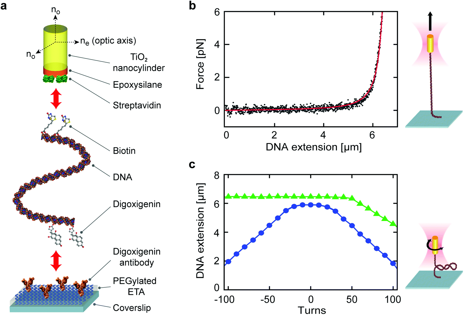 | ||
| Fig. 5 Application of DNA-tethered single-crystal rutile TiO2 nanocylinders in an OTW. (a) Schematic of a DNA tethered at one extremity to a single-crystal rutile TiO2 nanocylinder and at the other extremity to a flow cell channel surface. For the nanocylinder, the orientations of ordinary (no) and extraordinary (ne) refractive indices are indicated. First, we functionalize the flow cell channel surface with ETA, PEG, and digoxigenin antibodies. Then the end of the DNA containing the digoxigenin-enriched handle is attached to the flow cell channel surface via antigen–antibody binding. The other extremity of the DNA that contains the biotin-enriched handle binds to the streptavidin-coated nanocylinder. (b) The extension of tethered DNA as a function of force. The gray dots represent force-extension data while the red line is a fit to the WLC model. The illustration depicts a fully stretched DNA. (c) The response of DNA to rotation at different stretching forces (blue circles and green triangles for 0.5 pN and 1.8 pN, respectively). The corresponding illustration represents a supercoiled DNA. | ||
Prior to performing measurements on these DNA-tethered single-crystal TiO2 nanocylinders in an OTW (ESI Methods†), we calibrate the optical trap by using individual non-tethered nanocylinders to measure its trap stiffness (Fig. S7†). We can then apply a force to a tethered nanocylinder and stretch the DNA (Fig. 5b). The obtained force-extension data are fitted to the worm-like chain (WLC) model48 (red line in Fig. 5b) and yield a persistence length of 45 ± 1 nm and a contour length of 6.8 ± 0.2 μm (means and standard deviations for n = 5 different DNA tethers), in excellent agreement with previous reports.30,31,48 We additionally rotate the nanocylinder at low constant force (0.5 pN) or medium constant force (1.8 pN) to supercoil the tethered DNA molecule. The resulting extension–rotation relationship (Fig. 5c) shows the characteristic symmetric (asymmetric) response of twisted DNA in the low (medium) force regime, also in agreement with previous reports.31,49–52 We note that the OTW provides an excellent platform to evaluate the quality of our top-down fabrication of single-crystal TiO2 nanostructures, as only nanocylinders with precisely controlled dimensions and uniformity are appropriate for stable and reproducible optical trapping. Furthermore, the use of the OTW to stretch and twist DNA molecules provides a stringent test of the applied surface functionalization, as these processes (notably twisting) are only possible provided that the surface functionalization and bioconjugation processes are sufficiently efficient to allow for the formation of multiple stable bonds at either DNA extremity.52
Conclusions
We have developed and optimized processes for the fabrication, surface functionalization, and bioconjugation of single-crystal TiO2 nanostructures and nanoparticles. Using two top-down etching approaches, we demonstrate the fabrication of highly uniform nanostructures and nanoparticles with controllable shapes and dimensions. The CHF3-based etching process provides a wider range of etch geometries, while the SF6-based etching process results in improved surface quality allowing homogeneous and dense coating. We are able to etch single-crystal TiO2 into various nanoscale shapes, including cylinders, cones, and hourglass-shaped structures. The fabricated nanostructures have diameters in the range of 100–600 nm, with heights up to 1–2 μm under etching conditions that yield high etch rate and selectivity. Using SF6-etched single-crystal TiO2 nanocylinders, we show how they can be functionalized with high efficiency and be conjugated covalently to a majority of biomolecules. We demonstrate the use of these coated TiO2 nanocylinders by stretching and twisting individually tethered DNA molecules, an application that exploits the tight dimensional control and high quality surface functionalization of nanocylinders etched from a rutile (100) single-crystal TiO2 substrate. Our developed fabrication and surface functionalization methods will likely find utilization in diverse optical and electronic applications of single-crystal TiO2, including applications in life science-oriented fields through e.g. the development of biosensors and single-molecule techniques.Methods
Fabrication and bioconjugation of single-crystal rutile TiO2 nanocylinders for OTW experiments
We use single-side polished single-crystal rutile TiO2 (100) substrates (Latech, Singapore), 10 × 10 mm2 in size and 0.5 mm in thickness, to produce nanocylinders. We clean the substrates in fuming nitric acid (99.5%, Sigma-Aldrich, The Netherlands) using ultrasonication for 10 min followed by thorough rinsing in DI water and drying under a nitrogen (N2) stream (Fig. 1, step 1). We then subject the substrates to an O2 plasma (TePla300, PVA TePla, Germany), after which we spin-coat a ∼250 nm-thick e-beam resist layer (PMMA 950k A4, MicroChem, Germany) at 500 rpm for 5 s and then 3000 rpm for 55 s. We bake the resist-coated substrates on a hotplate for 30 min at 175 °C (Fig. 1, step 2). The substrates do not require an additional conductive layer to prevent charge accumulation during e-beam patterning since it has sufficiently high electrical conductivity.We then use an e-beam patterning system (EBPG 5000+, Leica, UK; the acceleration voltage is set to 100 kV and the aperture diameter to 400 μm) to pattern the PMMA layer by a defocused e-beam with circular cross-section and tunable diameter. The patterning of each circular shape is performed by a single-pixel e-beam exposure, defining the shapes of the Cr mask for subsequent nanocylinder etching. Using optimized e-beam conditions (a current of 85 nA, a defocusing of 100–200 nm, and a dose of 2000 μC cm−2), we pattern circles with 600 nm pitch on a circular patterning area with radius ∼4 mm (∼140 million masks in total) in <30 min. We develop the patterned substrate using a solution of methyl isobutyl ketone (MIBK, Sigma-Aldrich, The Netherlands) and isopropyl alcohol (IPA, Sigma-Aldrich, The Netherlands) (1:3 MIBK:IPA) for 60 s with constant hand agitation at room temperature. We then rinse the substrate in IPA for 30 s and dry it under a N2 stream (Fig. 1, step 3).
We deposit the Cr mask layer using either an e-beam evaporator (Temescal FC-2000, Ferrotec, Germany) or a thermal evaporator (L560, Leybold Heraeus, Germany) loaded with Cr pieces (purity of 99.95%, Kurt J. Lesker, Germany), using the patterned PMMA layer as evaporation windows. We use slow Cr deposition rates (≤1.0 Å s−1) to obtain high quality Cr layers (Fig. 1, step 4). We finalize Cr mask formation in a lift-off process by soaking the substrate into a preheated (80 °C) resist stripper (PRS-3000, JTBaker, The Netherlands) for 20 min with constant agitation using a magnetic spinner. Then we thoroughly rinse the substrate in DI water and dry it under a N2 stream (Fig. 1, step 5).
We etch TiO2 nanocylinders using the optimized conditions (Table S2†) for vertical sidewall angles (Fig. 1, step 6). We etch nanocylinders with either an RIE system (Fluor Z401S, Leybold Heraeus, Germany; Fig. 2a and b) or an ICP-RIE system (Plasmalab system 100, Oxford Instr., UK; Fig. 2f). For dimensional analysis of the etched nanocylinders, we employ SEM systems (Hitachi S4800 FESEM, FEI XL30S FEG SEM, or FEI Nova NanoSEM). We remove the used Cr mask using a wet etchant (Chromium Etchant N° 1, MicroChemicals, Germany) and then perform surface cleaning using fuming nitric acid and O2 plasma (TePla300) for the subsequent surface functionalization (Fig. 1, step 7).
Optionally, if area-selective functionalization on top of the nanocylinders is required, we cover their sidewalls with a temporary protection layer. We cover the substrate with a PMMA 950k resist at a chosen concentration to provide a spin-coated thickness larger than the heights of the nanocylinders (Fig. 1, step 8). Consequently, we etch the PMMA layer to render the tops of the nanocylinders accessible, using either O2 plasma (TePla300) or a MIBK solution (Fig. 1, step 9). Note that we do not bake the resist in order to allow for its straightforward removal afterwards.
To attach biomolecules to TiO2 nanocylinders, we first activate the nanocylinder substrates by O2 plasma treatment (Plasma-PREEN I, Plasmatic Systems Inc., USA). Then we bind GPDMES to the substrate for 15 min at 75 °C using non-diluted GPDMES solution, and wash the substrate in chloroform (CHROMASOLV plus, for HPLC, ≥99.9%, Sigma-Aldrich, The Netherlands) three times for 15 s each, followed by drying under a N2 stream (Fig. 1, step 10). (If a temporary PMMA layer is used for area-selective functionalization, we first wash the substrate in ethanol three times for 15 s each directly after the incubation with GPDMES, followed by drying under a N2 stream. We then remove the temporary PMMA layer in chloroform for 15 min at room temperature, followed by an additional washing in fresh chloroform three times for 15 s each and drying under a N2 stream.)
We then bind streptavidin molecules to the epoxy group of GPDMES by incubating the nanocylinders with 2 μM streptavidin (Sigma-Aldrich, The Netherlands) in PBS solution (pH 7.4, Sigma-Aldrich, The Netherlands) for 1 h at room temperature. After washing the substrate three times for 15 s each with PBS/TWEEN® solution (pH 7.4, PBS containing 0.1% (v/v) TWEEN® 20 (Sigma-Aldrich, The Netherlands)), we wash the substrate with PBS solution (pH 7.4) another three times for 15 s each (Fig. 1, step 11).
We cleave TiO2 nanocylinders mechanically from the substrate using a diamond microtome blade (DT315D50, C.L. Sturkey, USA) inside a PBS/Triton™ droplet (pH 7.4, PBS containing 0.05% (v/v) Triton™ X-100 (Sigma-Aldrich, The Netherlands)), followed by suction of the droplet using a micropipette (Fig. 1, step 12). These cleaved, streptavidin-coated TiO2 nanocylinders can be further coupled with biomolecules of interest, e.g. DNA with biotinylated handles, by incubating them in a flow cell channel for OTW experiments (ESI Methods†).
Acknowledgements
We acknowledge Z. Huang for his initial help in TiO2 fabrication and M. Zuiddam, C. de Boer, M. van der Krogt, A. van Run, A. van Langen-Suurling, H. Miro, R. Mattern, Y. Caspi, and M. Jonsson for helpful discussions and advice on fabrication steps. We also thank T. van Laar for the preparation of DNA constructs, J. Kerssemakers, M. Docter, and V. M. Lizarraga for helpful discussions on the OTW setup, M. Ganji and O. Ordu for support in testing the surface functionalization protocol, J. van der Does and D. de Roos for the production of custom-made mechanical parts for the OTW setup and nanocylinder-cleaving tools, S. Khaiboulov for his help with laboratory infrastructure, and B. A. Berghuis and S. Pud for reviewing the manuscript. This research is supported by NanoNextNL, a micro and nanotechnology consortium of the Government of the Netherlands and 130 partners, and the Foundation for Fundamental Research on Matter (FOM), which is part of the Netherlands Organisation for Scientific Research (NWO), and by the European Research Council (ERC) via the DynGenome project (N° 312221).References
- G. Wang, H. Wang, Y. Ling, Y. Tang, X. Yang, R. C. Fitzmorris, C. Wang, J. Z. Zhang and Y. Li, Nano Lett., 2011, 11, 3026–3033 CrossRef CAS PubMed.
- H. Yu, K. Zhang and C. Rossi, Indoor Built Environ., 2007, 16, 529–537 CrossRef CAS.
- S. Hwang, H. Kwon, S. Chhajed, J. W. Byon, J. M. Baik, J. Im, S. H. Oh, H. W. Jang, S. J. Yoon and J. K. Kim, Analyst, 2013, 138, 443–450 RSC.
- E. Gale, Semicond. Sci. Technol., 2014, 29, 104004 CrossRef.
- W. S. Shih, S. J. Young, L. W. Ji, W. Water and H. W. Shiu, J. Electrochem. Soc., 2011, 158, H609–H611 CrossRef CAS.
- X. Liu, M. Guo, J. Cao, J. Lin, Y. H. Tsang, X. Chen and H. Huang, Nanoscale Res. Lett., 2014, 9, 1–5 CrossRef PubMed.
- Y. Tang, Y. Zhang, J. Deng, D. Qi, W. R. Leow, J. Wei, S. Yin, Z. Dong, R. Yazami, Z. Chen and X. Chen, Angew. Chem., Int. Ed., 2014, 53, 13488–13492 CrossRef CAS PubMed.
- Y. Tang, Y. Zhang, X. Rui, D. Qi, Y. Luo, W. R. Leow, S. Chen, J. Guo, J. Wei, W. Li, J. Deng, Y. Lai, B. Ma and X. Chen, Adv. Mater., 2016, 28, 1567–1576 CrossRef CAS PubMed.
- J. D. B. Bradley, C. C. Evans, J. T. Choy, O. Reshef, P. B. Deotare, F. Parsy, K. C. Phillips, M. Lončar and E. Mazur, Opt. Express, 2012, 20, 23821–23831 CrossRef CAS PubMed.
- X. Wang, M. Fujimaki and K. Awazu, Opt. Express, 2005, 13, 1486–1497 CrossRef CAS PubMed.
- A. Jannasch, A. F. Demirors, P. D. J. van Oostrum, A. van Blaaderen and E. Schäffer, Nat. Photonics, 2012, 6, 469–473 CrossRef CAS.
- P. A. Morris Hotsenpiller, J. D. Bolt, W. E. Farneth, J. B. Lowekamp and G. S. Rohrer, J. Phys. Chem. B, 1998, 102, 3216–3226 CrossRef.
- R. Wang, N. Sakai, A. Fujishima, T. Watanabe and K. Hashimoto, J. Phys. Chem. B, 1999, 103, 2188–2194 CrossRef CAS.
- J. M. Baik, M. H. Kim, C. Larson, X. Chen, S. Guo, A. M. Wodtke and M. Moskovits, Appl. Phys. Lett., 2008, 92, 242111 CrossRef.
- X. Feng, K. Zhu, A. J. Frank, C. A. Grimes and T. E. Mallouk, Angew. Chem., 2012, 124, 2781–2784 CrossRef.
- Z.-F. Bi, L. Wang, X.-H. Liu, S.-M. Zhang, M.-M. Dong, Q.-Z. Zhao, X.-L. Wu and K.-M. Wang, Opt. Express, 2012, 20, 6712–6719 CrossRef CAS PubMed.
- K. Awazu, M. Fujimaki, Y. Ohki and T. Komatsubara, Radiat. Meas., 2005, 40, 722–729 CrossRef CAS.
- A. M. Agarwal, L. Liao, J. S. Foresi, M. R. Black, X. Duan and L. C. Kimerling, J. Appl. Phys., 1996, 80, 6120–6123 CrossRef CAS.
- A. Stone, H. Jain, V. Dierolf, M. Sakakura, Y. Shimotsuma, K. Miura, K. Hirao, J. Lapointe and R. Kashyap, Sci. Rep., 2015, 5, 10391 CrossRef CAS PubMed.
- J. Lipfert, M. M. van Oene, M. Lee, F. Pedaci and N. H. Dekker, Chem. Rev., 2015, 115, 1449–1474 CrossRef CAS PubMed.
- Y. Wang, Y. He, Q. Lai and M. Fan, J. Environ. Sci., 2014, 26, 2139–2177 CrossRef PubMed.
- Y. Tang, Y. Zhang, J. Deng, J. Wei, H. Le Tam, B. K. Chandran, Z. Dong, Z. Chen and X. Chen, Adv. Mater., 2014, 26, 6111–6118 CrossRef CAS PubMed.
- Z. Miao, D. Xu, J. Ouyang, G. Guo, X. Zhao and Y. Tang, Nano Lett., 2002, 2, 717–720 CrossRef CAS.
- Y. Huang, G. Pandraud and P. M. Sarro, Nanotechnology, 2012, 23, 485306 CrossRef PubMed.
- E. Shkondin, J. Michael-Lindhard, M. D. Mar, F. Jensen and A. Lavrinenko, presented in part at the 15th Int'l Conf. on Atomic Layer Deposition, Portland, United States, June 2015.
- H. Y. Jeong, J. Y. Lee and S.-Y. Choi, Appl. Phys. Lett., 2010, 97, 42109 CrossRef.
- J. Dekker, K. Kolari and R. L. Puurunen, J. Vac. Sci. Technol., B, 2006, 24, 2350–2355 CAS.
- F. Karouta, J. Phys. D: Appl. Phys., 2014, 47, 233501 CrossRef.
- J. Tang, Y. Wang, J. Li, P. Da, J. Geng and G. Zheng, J. Mater. Chem. A, 2014, 2, 6153–6157 CAS.
- M. D. Wang, H. Yin, R. Landick, J. Gelles and S. M. Block, Biophys. J., 1997, 72, 1335–1346 CrossRef CAS PubMed.
- Z. Huang, F. Pedaci, M. Van Oene, M. J. Wiggin and N. H. Dekker, ACS Nano, 2011, 5, 1418–1427 CrossRef CAS PubMed.
- S. P. Pujari, L. Scheres, A. T. M. Marcelis and H. Zuilhof, Angew. Chem., Int. Ed., 2014, 53, 6322–6356 CrossRef CAS PubMed.
- W.-J. Kim, S. Kim, B. S. Lee, A. Kim, C. S. Ah, C. Huh, G. Y. Sung and W. S. Yun, Langmuir, 2009, 25, 11692–11697 CrossRef CAS PubMed.
- Y. Wang, J. Miao, Y. Tian, C. Guo, J. Zhang, T. Ren and Q. Liu, Opt. Express, 2011, 19, 17390–17395 CrossRef CAS PubMed.
- R. Kaliasas, J. Baltrusaitis, M. Mikolajūnas, L. Jakučionis and D. Viržonis, Thin Solid Films, 2012, 520, 2041–2045 CrossRef CAS.
- A. P. Milenin, C. Jamois, T. Geppert, U. Gösele and R. B. Wehrspohn, Microelectron. Eng., 2005, 81, 15–21 CrossRef CAS.
- K. Suzuki, S.-W. Youn, Q. Wang, H. Hiroshima and Y. Nishioka, Microelectron. Eng., 2013, 110, 432–435 CrossRef CAS.
- A. Somashekhar, H. Ying, P. B. Smith, D. B. Aldrich and R. J. Nemanich, J. Electrochem. Soc., 1999, 146, 2318–2321 CrossRef CAS.
- K. Mohamed and M. M. Alkaisi, Nanotechnology, 2013, 24, 015302 CrossRef CAS PubMed.
- K. P. Giapis, G. R. Scheller, R. A. Gottscho, W. S. Hobson and Y. H. Lee, Appl. Phys. Lett., 1990, 57, 983–985 CrossRef CAS.
- U. Diebold, Surf. Sci. Rep., 2003, 48, 53–229 CrossRef CAS.
- S. D. Chandradoss, A. C. Haagsma, Y. K. Lee, J.-H. Hwang, J.-M. Nam and C. Joo, J. Visualized Exp., 2014, 86, e50549 Search PubMed.
- H. Li, X. Zhang, X. Zhang, K. Wang, H. Liu and Y. Wei, ACS Appl. Mater. Interfaces, 2015, 7, 4241–4246 CAS.
- L. Chen, B. Yang and J. Zhang, J. Adhes. Sci. Technol., 2014, 28, 1725–1738 CrossRef CAS.
- Y. Nam, D. W. Branch and B. C. Wheeler, Biosens. Bioelectron., 2006, 22, 589–597 CrossRef CAS PubMed.
- Z. Ji, X. Jin, S. George, T. Xia, H. Meng, X. Wang, E. Suarez, H. Zhang, E. M. V. Hoek, H. Godwin, A. E. Nel and J. I. Zink, Environ. Sci. Technol., 2010, 44, 7309–7314 CrossRef CAS PubMed.
- B. Sweryda-Krawiec, H. Devaraj, G. Jacob and J. J. Hickman, Langmuir, 2004, 20, 2054–2056 CrossRef CAS PubMed.
- C. Bouchiat, M. D. Wang, J.-F. Allemand, T. Strick, S. M. Block and V. Croquette, Biophys. J., 1999, 76, 409–413 CrossRef CAS PubMed.
- D. A. Koster, V. Croquette, C. Dekker, S. Shuman and N. H. Dekker, Nature, 2005, 434, 671–674 CrossRef CAS PubMed.
- B. Gutiérrez-Medina, J. O. L. Andreasson, W. J. Greenleaf, A. Laporta and S. M. Block, Methods Enzymol., 2010, 475, 377–404 Search PubMed.
- P.-C. Li, J.-C. Chang, A. La Porta and E. T. Yu, Nanotechnology, 2014, 25, 235304 CrossRef PubMed.
- T. R. Strick, J.-F. Allemand, D. Bensimon, A. Bensimon and V. Croquette, Science, 1996, 271, 1835–1837 CAS.
Footnote |
| † Electronic supplementary information (ESI) available: Experimental details (ESI Methods) of the optic axis orientation of TiO2 nanocylinders, Cr etch mask fabrication, surface functionalization and its evaluation using fluorescence microscopy, preparation of DNA constructs, assembly of flow cells, bioconjugation of TiO2 nanocylinders, OTW instrumentation and measurements; TiO2 dry etching optimization and the etching parameters employed (Tables S1 and S2); dimensional analysis of TiO2 nanocylinders (Table S3); diverse applications of TiO2 at the nanoscale (Fig. S1); selection of etch mask material (Fig. S2); control of sidewall profiles in TiO2 etching (Fig. S3); size distributions of TiO2 nanocylinders (Fig. S4); quantitative comparisons of different surface linker molecules (Fig. S5); DLS measurements on TiO2 nanocylinders (Fig. S6); optical trap calibration (Fig. S7); and supplementary references. See DOI: 10.1039/c6nr00898d |
| This journal is © The Royal Society of Chemistry 2016 |