
 Open Access Article
 This Open Access Article is licensed under a
 Creative Commons Attribution 3.0 Unported Licence
Impedance spectra of Fe-doped SrTiO3 thin films upon bias voltage: inductive loops as a trace of ion motion
S.
Taibl
*,
G.
Fafilek
and
J.
Fleig
Institute of Chemical Technologies and Analytics, Vienna University of Technology, Getreidemarkt 9-164/EC, 1060 Vienna, Austria. E-mail: stefanie.taibl@tuwien.ac.at
First published on 18th April 2016
Abstract
Mass and charge transport properties of slightly Fe-doped SrTiO3 (Fe:STO) thin films on a conducting substrate were investigated by means of impedance spectroscopy under different bias voltages and I–V measurements with varying scan rates. At measurement temperatures between 325 °C and 700 °C the applied bias voltage caused an unusual “inductive loop” in the low frequency range of impedance spectra. DC measurements showed that current–voltage curves strongly depend on the scan rate, indicating that different states of the sample became accessible to probe. Both findings can be understood in terms of bias induced ion motion, i.e. by stoichiometry polarization within the Fe:STO thin films upon voltage. Hence, the appearance of an “inductive loop” in the impedance spectra is considered a very general feature that might exist for many materials, particularly in oxide thin films. It may indicate ion motion and stoichiometry variations taking place in the corresponding frequency range.
1. Introduction
SrTiO3 is among the most investigated electroceramic materials and often acts as a kind of large band gap model oxide, representing many of the features found in more complex perovskites such as ferroelectric BaTiO3 or Pb(Zr,Ti)O3. Its bulk defect chemistry is well understood with thermodynamic and kinetic data available for many conditions.1–8 In Fe-doped SrTiO3, for example, the acceptor dopant is compensated by oxygen vacancies and electron holes with the individual concentrations depending on the oxygen partial pressure and temperature.3 Also interfaces in SrTiO3 have been investigated in great detail.6,9 Grain boundaries of acceptor doped SrTiO3 are characterized by a positive core and adjacent space charge layers with strong depletion of positive charge carriers, i.e. holes and oxygen vacancies. This causes a significant grain boundary resistance for electron transport10–12 and also for chemical diffusion of oxygen13,14 or stoichiometry polarization upon field load, where ion motion is essential.15 Similar space charge layers could be detected at surfaces, causing an additional resistance for oxygen exchange with the gas atmosphere, and at electrodes (Schottky contacts).16,17Recently, thin SrTiO3 films came into the focus of research. In general, thin films of perovskite-type oxides may exhibit defect chemical properties that differ from bulk behavior of macroscopic samples.18–24 This might not only be caused by the high density of interfaces but also by structural differences, with strain possibly playing a significant role.22–24 Substantial differences between bulk defect concentrations and those of thin films were also found for SrTiO3.25,26 Finite-size effects and space charges were discussed as possible reasons but a detailed understanding of these deviations is still missing. Moreover, SrTiO3 thin films exhibit a voltage induced resistance switching behavior.27–32 Thus, they are also promising systems (and again model materials) for memory devices based on memristors.
The bias induced switching of the resistance has to involve ion motion and there is an ongoing discussion about the underlying mechanisms of the very fast switching behavior even at room temperature.29,33,34 Explanations of the switching behavior are often based on the model of field driven stoichiometry polarization of acceptor-doped oxides: in SrTiO3 with one or two electrodes blocking the ion flow, while both electrodes being reversible for electrons, any applied voltage has to cause a gradient in the chemical potential of oxygen within the sample. Thus an inhomogeneous composition, i.e. a spatially varying δ(x) in SrTiO3−δ, and therefore inhomogeneous mass and charge transport properties results. Those may not only cause high resistive but also low resistive situations, depending on the specific δ(x) value.
A quantitative model of the steady state resulting from such a stoichiometry polarization with one ionically reversible electrode was developed by C. Wagner35 and is often referred to as the Wagner–Hebb polarization. Time dependent stoichiometry polarization with two blocking electrodes could successfully explain the phenomenon of long-term resistance degradation in SrTiO3 and BaTiO3.36,37 In further studies the local conductivities in SrTiO3 single crystals and polycrystals were measured after such a stoichiometry polarization and strongly varying conductivity was found within the samples with high electron conductivity near to the (former) cathode and high hole conductivity at the other electrode.38,39 Even conductivity profiles within single grains could be detected. Stoichiometry changes upon voltage load are also often assumed to be essential for resistive switching in polarized thin films, with additional phenomena causing very fast localized switching behavior in many cases.30,32
In view of the memristor applications, also from a more fundamental point of view, it is important to understand better the defect chemistry and the change of charge transport properties in SrTiO3 thin films. This not only concerns films in equilibrium with the gas phase, but also films with frozen-in defect chemical situations and films supposedly in non-equilibrium due to an applied electric field. Two important methods for analyzing the charge transport properties of electroceramics are impedance spectroscopy and current–voltage (I–V) measurements, the latter either probing steady state situations or analyzing transient variations of current or voltage.
In this study, both methods were applied to slightly Fe-doped SrTiO3 thin layers on conducting substrates in order to investigate mass and charge transport in such films. Special emphasis is put on transient effects caused by a bias load at elevated temperatures (325–700 °C). At such temperatures, it is not only possible to induce bias driven changes but also to quickly regenerate equilibrium situations, thus enabling very reproducible and systematic studies. A major outcome of these measurements is the fact that bias induced ion motion in the thin films often leads to inductive loops in impedance spectra. This correlation of inductive loops and stoichiometry polarization should be a very general feature of many oxide thin films mostly overlooked or ignored so far. Thus, our experiments and the corresponding quantitative model may also have a significant impact on impedance studies in electroceramics in general.
2. Experimental
SrTiO3 thin films of 100–413 nm thickness were deposited by pulsed laser deposition (PLD) from the target material with nominally 0.4 mol% Fe doping (Fe:STO) prepared by the mixed oxide route (sintering temperature = 1200 °C). The films were deposited on single crystalline Nb-doped SrTiO3 substrates (Nb:STO, 0.5 wt% Nb, 0.5 mm thickness, Crystec, Germany) at substrate temperatures of Tsubstrate = 650 °C, an oxygen partial pressure of 0.15 mbar, an excimer laser wavelength of 248 nm and a pulse rate of 5 Hz. Subsequent ICP-OES (inductively coupled plasma optical emission spectrometry) of dissolved pieces of the target material revealed a true doping level of 0.37 mol%. The exact Fe content in the thin film was not analyzed, but preliminary studies on films with other acceptor dopants (Al, Ni) and different dopant concentrations indicated that the phenomena reported here are a rather general behavior and not specific for the given Fe content. Transmission electron microscopy studies on the films showed epitaxial growth without any indication of grain boundaries or pores (Fig. 1a and b). Investigation of the surface by means of atomic force microscopy (AFM) revealed a very smooth surface with an average roughness of 0.2 nm (Fig. 1c), which also indicates quite undisturbed growth of the layers.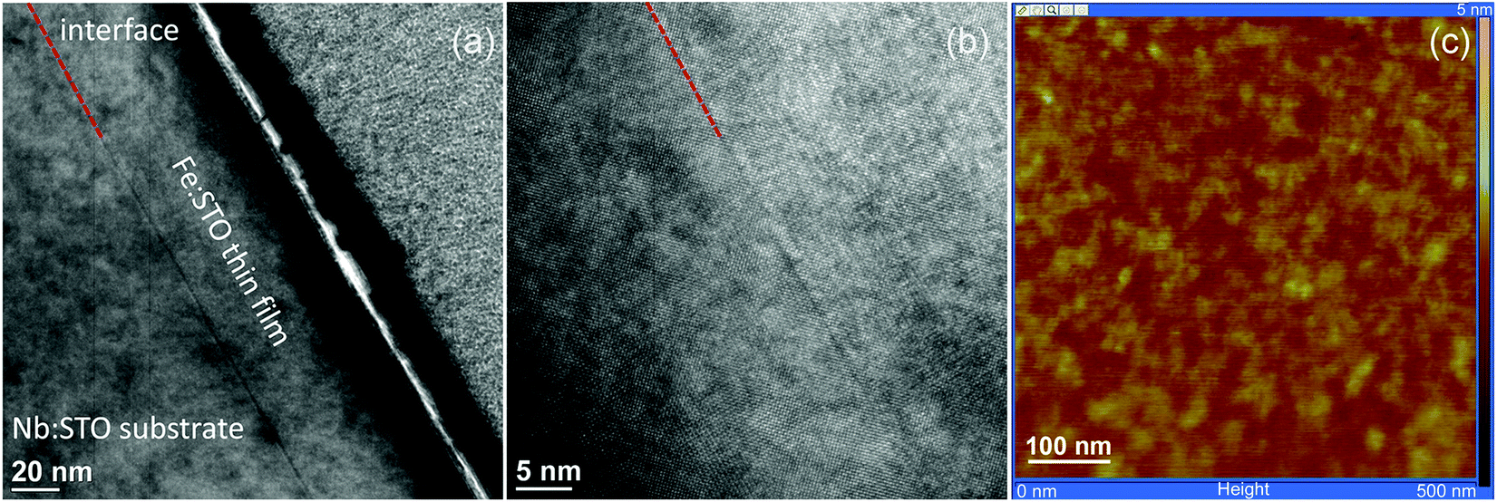 | ||
| Fig. 1 (a) and (b) TEM images (two different magnifications) of a Fe:STO thin film deposited on Nb:STO. The dotted red line in (a) and (b) indicates the interface. Neither grain boundaries nor dislocations were found in such films. (c) Investigations by means of AFM showed a very smooth surface of these layers, with an average roughness of 0.2 nm. | ||
The highly conducting Nb:STO substrate acted as a counter electrode in all electrical measurements. It is at least partially reversible for electrons but supposedly completely blocking for oxide ions due to its negligible oxygen vacancy concentration. As the top (working) electrode, a 100 nm (La0.6Sr0.4)CoO3−δ (LSC) thin film was prepared by PLD; preparation details are given in ref. 40. Circular microelectrodes of 100–300 μm diameter were fabricated from the LSC layer by photolithographic techniques and chemical etching in diluted HCl solution. An example of such a sample is shown in Fig. 2a. LSC (micro-)electrodes were used since this mixed conductor is known to be an excellent oxygen exchange material and therefore often employed as an electrode in solid oxide fuel cells.41–43 In our case, it serves as an electrode that is supposedly rather reversible for ions via the oxygen exchange reaction O2− ↔ 1/2O2 + 2e− at the surface of LSC. This is essential in steady state I–V measurements and ensures that the chemical potential of the gas atmosphere is also present at the SrTiO3|LSC interface.
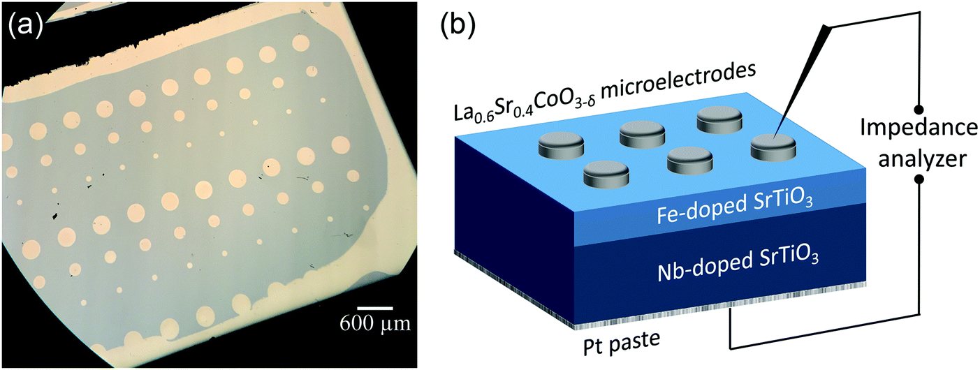 | ||
| Fig. 2 (a) Top view image of a sample with (La0.6Sr0.4)CoO3−δ (LSC) microelectrodes of different diameters. (b) Schematic sketch of the Fe:STO thin film, sandwiched between an oxygen blocking electrode (Nb:STO substrate) and a reversible electrode (LSC microelectrodes). | ||
On the bottom side of the Nb:STO substrate a Pt paste electrode was deposited and the LSC microelectrodes were made to come in contact with Pt/Ir tips for impedance and I–V measurements. A sketch of a sample cross section is shown in Fig. 2b. In the following, polarity notions refer to the polarity of the LSC top electrode (vs. bottom counter electrode = substrate), in agreement with the notion used in most papers on resistive switching. One has to keep in mind that a negative voltage (at the LSC top electrode) corresponds to a positive voltage and thus higher chemical potential of oxygen at the ion blocking Nb:STO.
All samples were measured in ambient air within a temperature range between 325 °C and 700 °C. The measurements presented in this paper were partly conducted in a set-up with homogeneous heating (Tcorr) while other measurements were performed on a heating stage with sample heating from the bottom side (Tset).44 The given temperatures are thus either the correct sample temperatures (Tcorr) or the slightly higher set temperature of the heating stage (Tset). Except from the less accurate temperature measurement and a certain thermovoltage in the latter case, no set-up dependent results were found, and all effects were completely reproducible. The use of microelectrodes minimized the risk of pin-holes in the relevant part of the SrTiO3 films and allowed for numerous measurements on one and the same film. Reproducibility was excellent for each film though slight differences were found on different films, see Results and discussion.
All samples were heated up to a certain temperature and were held under these conditions for a few minutes before impedance measurements were started. Impedance spectra were measured in the frequency range of 1 MHz to 100 mHz (starting at high frequencies) with and without bias load (maximum value: ± 500 mV) using an Alpha-analyzer with POT/GAL-interface from Novocontrol (Novocontrol, Germany) operating at an AC rms amplitude of 20 mV. I–V measurements were also conducted by means of the same instrumental set-up from Novocontrol. I–V curves were recorded with different scan rates, from very slow with one complete cycle taking several hours to ensure steady state condition for each voltage, to rather fast curves (up to 25 Hz cycling frequency). Before starting I–V cycles, a steady state was established by applying the starting voltage for an appropriate time (depending on temperature). Moreover, systematic potentiostatic resistance measurements were performed (voltage typically up to a few 100 mV), together with resistance relaxation measurements after switching off the large voltage.
3. Results and discussion
3.1 Bias dependence of impedance spectra
Fig. 3a displays impedance spectra for four different Fe:STO film thicknesses, measured at 600 °C (Tcorr). While the main part of the spectra found for thinner films is rather semicircle-like, the thickest film clearly exhibits deviations from an ideal single arc. Moreover, an additional small arc-like element was often found at low frequencies. The latter is attributed to electrode effects and is not further considered in this paper. The almost linear relationship of the low frequency resistance and the film thickness indicates that the entire film contributes to the impedance; the resistance is not largely caused by interfacial regions close to the electrodes. This is further confirmed by an analysis of the capacitance of the main arc. This scales with the inverse film thickness and yields values close to those expected from the geometrical (bulk) capacitance of SrTiO3 at moderate temperatures.12 Space charges at electrodes should neither depend on the film thickness nor yield a meaningful bulk permittivity value. Hence, they seem to be of minor importance here.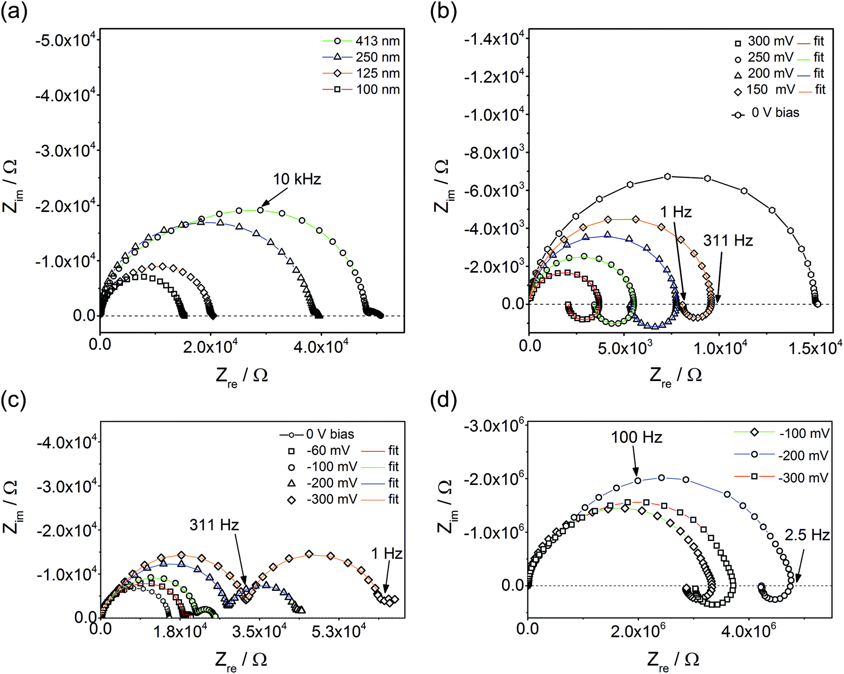 | ||
| Fig. 3 (a) Impedance spectra of four STO films with varying thickness, measured at 600 °C (Tcorr) on 300 μm LSC microelectrodes. The film resistance scales almost linearly with thickness. Some minor changes in the shape of the spectra can be observed with increasing film thickness. (b) Spectra of a 160 nm STO thin film measured at 600 °C (Tcorr) for positive bias voltages; an “inductive loop” appears for all measurements. (c) For this 160 nm STO film, an additional semicircle appears upon negative bias voltage (Tcorr = 600 °C). (d) In other films (here again 160 nm thickness, measured at Tset = 500 °C) loops are also found for negative bias voltages. | ||
However, when calculating the film conductivity from the measured resistances, the obtained values are much smaller than the bulk conductivity determined from a polycrystal with the PLD target composition. At 550 °C (Tcorr), ca. 1.5 × 10⁻⁷ and 6.7 × 10⁻⁴ S cm−1 were found for thin films and macroscopic polycrystals (bulk part), respectively. Activation energies are also substantially different: thin films exhibit ca. 1.6 eV while the grain bulk of a polycrystal shows 0.95 eV, in excellent agreement with the literature.11 Thus, our measurements confirm that SrTiO3 thin films are very different from bulk SrTiO3, despite nominal epitaxy. Additionally, the deviations of the bulk arcs from ideal semicircles found in thicker films (see above) may indicate some chemical or structural inhomogeneities.
Analyzing and understanding these differences is highly desirable and additional information is available from our studies. Among others, preliminary oxygen tracer studies also revealed very low ionic conductivity, and we suggest that space charge layers along extended one-dimensional defects (dislocations) cause a strong decrease of the mobile charge carrier concentrations in the entire film and thus lead to a low electronic and even lower ionic conductivity. The approach of explaining an increased sample resistance by means of overlapping space charge regions in nanomaterials is also used in ref. 18, 19 and 45. Further analysis of the exact defect chemical situation in such thin films, however, is beyond the scope of this paper. Here, the focus is on a basic understanding of the effects caused by an additional bias voltage. Accordingly, the following part of the paper deals with bias dependent impedance studies and I–V measurements.
Applying a bias voltage during impedance measurements leads to a drastic change of the impedance spectra. Not only does the main arc change its size and partly also its shape, but an additional impedance feature comes into play. Positive bias values cause an “inductive loop” (Fig. 3b) meaning that positive imaginary parts are found for lower frequencies and that the total impedance decreases with decreasing frequency. The relative importance of this inductive loop increases by increasing the bias voltage, also since the main high frequency arc shrinks. For negative bias, often an additional low frequency semicircle was observed which increases in size with larger voltage (Fig. 3c). In some films, also upon negative voltage loops can be found (Fig. 3d). For both negative bias cases (loop or second semicircle), the partly already existing slight splitting of the high frequency arc into two features, possibly due to film inhomogeneities, is intensified (Fig. 3c and d). All these additional features not only appear for a certain temperature and film thickness. Rather, highly reproducible properties of Fe:STO films were found in the entire temperature range from 325 °C to 700 °C.
This reproducible occurrence of inductive loops for positive bias voltage does not depend on the AC amplitude or the specific impedance analyzer, it can be definitely excluded that it is a measurement artefact in contrast to a loop found in impedance measurements between two microelectrodes.46–48 Rather, it has physical relevance, similar to inductive loops found in electrochemical studies of polarized electrodes in aqueous solutions.49,50 In the following, it is shown that such loops, or additional semicircles as their counterpart, might exist in many samples exhibiting stoichiometry polarization upon field load. The explanation of both features is based on the analysis of current–voltage characteristics performed with different scan rates.
3.2 Scan-rate dependent current–voltage measurements
Fig. 4 displays a very slowly measured current–voltage curve of a 180 nm thin SrTiO3 film, obtained at 420 °C (Tset) between +500 and −500 mV at a scan rate of 0.046 mV s−1 (23.2 μHz); reproducibility is proven by returning to the +500 mV value (complete cycle). Before starting at +500 mV, a steady state current was established by waiting for 30 minutes. In the positive voltage range the curve looks exponential while for negative voltages it is at least in some parts almost linear (see magnification in Fig. 4). Very similar curves are found for all films, all temperatures and all microelectrodes on a given film. Only the exact shape of the curve for negative voltages sometimes differed and included slight concave or convex bending. The slight offset for open circuit condition is due to asymmetric heating in this setup (thermovoltage). For further interpretation it is important that the very slow scan rate (cycle frequency) of the I–V curve corresponds to a frequency much lower than the lowest frequency used to collect complete impedance spectra. Accordingly, the slow current–voltage curve is the large signal counterpart of the low frequency real axis intercept of the inductive loops or of the additional semicircles in bias dependent impedance spectra.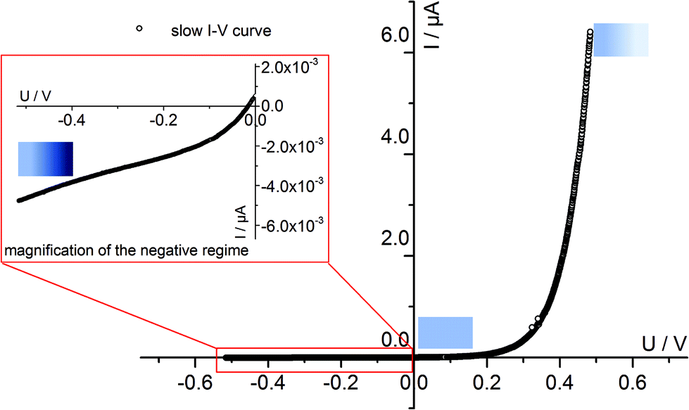 | ||
| Fig. 4 Slowly measured I–V curve with a scan rate of 0.046 mV s−1 (2.3 × 10⁻² mHz) for a 180 nm thin film at 420 °C (Tset). Prior to the scan, a steady state current was established for 500 mV by waiting for 30 minutes. There is no difference between forward and backward scan. The slight offset for zero current is due to a thermovoltage (asymmetric heating). The three sketched boxes indicate the gradient of the oxygen vacancy concentrations at different voltages for LSC on the left hand side of the sketched film (see Discussion, bright side = high oxygen vacancy concentration). | ||
In a second step, I–V curves were measured at a dramatically increased scan rate. Scan frequencies that correspond to the medium frequency real axis intercept of the impedance spectrum upon bias, i.e. a frequency before onset of the loop, are used in this case. Such an I–V curve, conducted at 420 °C (Tset) is displayed in Fig. 5a, together with the corresponding frequency (25 Hz = scan rate ∼4 × 10⁴ mV s−1) indicated in the impedance spectrum. Again, a steady state DC current at a certain starting voltage was established prior to the I–V scan; see changing current at 0.4 V in Fig. 5a.
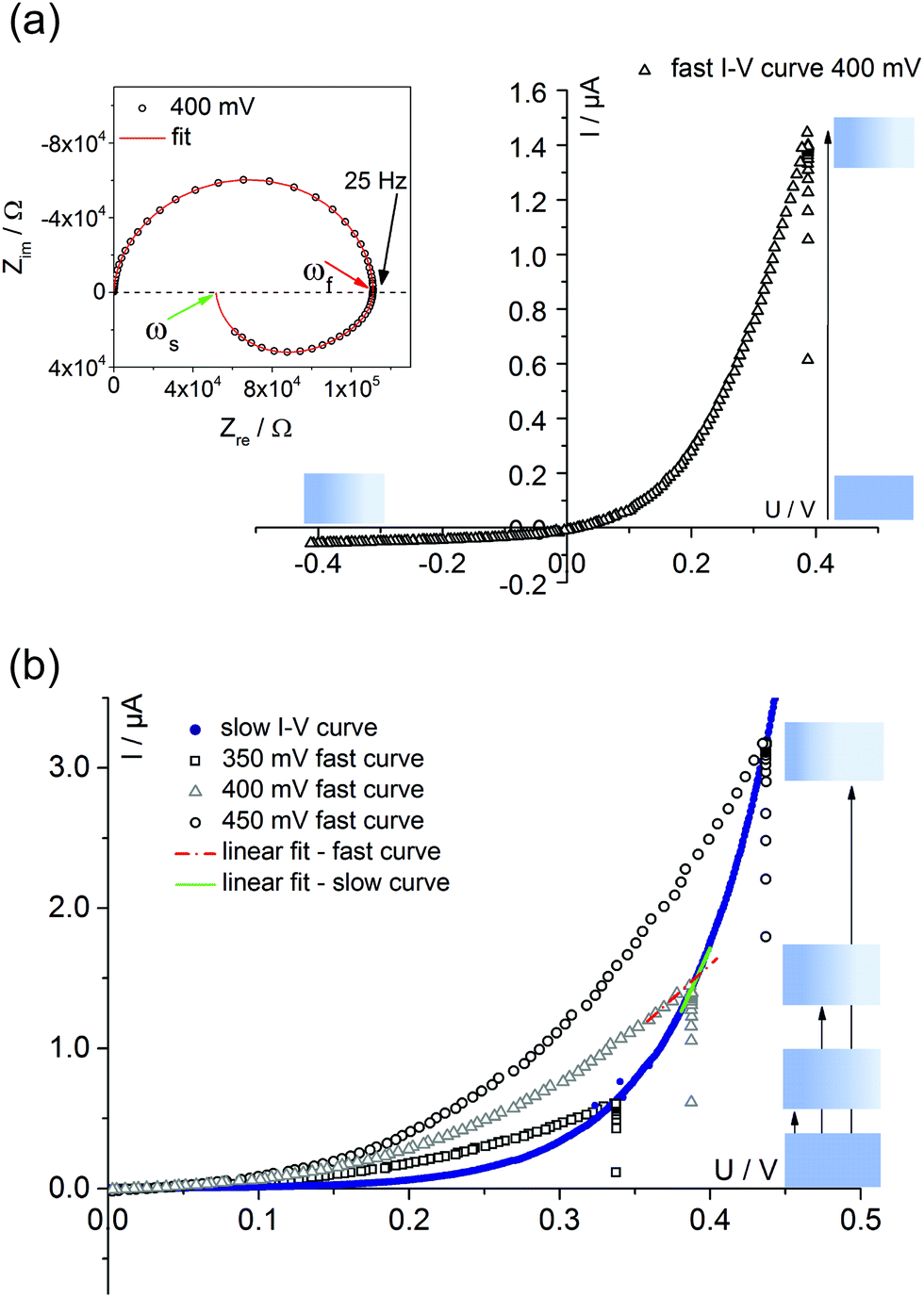 | ||
| Fig. 5 (a) Quickly measured I–V curve (scan rate of 4 × 10⁻⁴ mV s−1) of a 180 nm thin STO film at 420 °C (Tset) after first applying 400 mV for 10 minutes. The corresponding impedance spectrum upon 400 mV bias is also shown; the arrows indicate the frequencies corresponding to the scan rates of fast (ωf, red) and slow (ωs, green) I–V measurements. A fit according to the model discussed in section 4 is shown as well. (b) Comparison of a slow I–V curve (180 nm STO film, 420 °C = Tset) and three fast curves with different starting voltages. In all cases, a steady state for the starting voltage was first established. For a given starting voltage, slopes of fast and slow curves clearly differ. A quantitative analysis of the slopes is given in Table 1. | ||
In the following, we denote these current voltage curves “fast I–V curves” in contrast to the “slow I–V curve” shown in Fig. 4. A comparison of slow and fast I–V curves is depicted in Fig. 5b. Despite identical starting points, fast and slow curves substantially differ. For positive starting voltage, for example, the decrease of the current towards the origin is less sharp in the fast curve. Moreover, slow I–V curves are independent of the starting voltage while fast I–V curves strongly depend on the steady state established before measurement. Irrespective of the mechanistic reasons behind these scan rate dependent I–V curves, this knowledge is already sufficient to explain the appearance of inductive loops and second arcs in the bias dependent impedance spectra, see next section. A mechanistic explanation of the curve shapes and a quantitative model for analyzing the impedance spectra is given in section 4.
3.3 Relation between impedance spectra and I–V curves
Bias dependent impedance spectroscopy usually uses small AC voltages on top of a mostly much larger DC voltage. This corresponds to probing the slope of an I–V curve, see sketch in Fig. 5b. This slope of the I–V curve, however, depends on the scan rate. For the given example (positive starting voltage), the slope is larger for the slow I–V curve and thus the corresponding differential resistance is smaller. This finds its equivalent in the impedance spectrum: a larger resistance is found at intermediate frequencies compared to low frequencies.For a quantitative comparison, Table 1 displays four resistances for each bias voltage. First, the slope of the fast I–V curve is compared with the intermediate frequency intercept in the impedance spectrum (ωf in Fig. 5a). For all bias values, the agreement is rather good, showing that impedance spectroscopy indeed detects the slope of the I–V curve. Second, the extrapolation of the spectrum to its low frequency limit (ωs) leads essentially to the same resistance as the slope analysis of the slow I–V curve. This analysis indicates that the inductive loop is indeed caused by the larger differential resistance (smaller slope) of the fast I–V curve: a frequency range exists for which the impedance increases despite increasing frequency and this manifests itself as an “inductive loop”. Using the same arguments, one can also understand the appearance of an additional arc for negative starting voltage. Then, the slope of the fast I–V curve at a given voltage is larger than that of the slow curve.
Hence, the existence of scan rate dependent I–V curves is already sufficient to explain additional impedance features of bias dependent measurements and particularly the possibility of an inductive loop at low frequencies. In our specific case with almost exponential I–V curves, polarity is highly important for the question whether a loop or a second semicircle develops. However, the shape of the low frequency feature is not a consequence of polarity itself but of slopes and indeed in some cases loops also emerge for negative voltages (see Fig. 3d).
4. Mechanistic discussion and impedance model
4.1 Interpretation of slow and fast I–V curves
The question remains, why fast and slow I–V curves are different for our SrTiO3 thin films. This brings us back to the considerations in the Introduction. From theory and many experiments it is known that applying a voltage to a mixed conducting oxide causes stoichiometry polarization if one or two electrodes are blocking for ions. Oxide ions in our Fe:STO thin films are supposed to be blocked at the Nb:STO electrode, while the LSC electrode shows at least some reversibility for oxide ion exchange. Hence, upon voltage load a stoichiometry variation, i.e. build-up of a δ(x) can also be expected in our Fe:STO films, irrespective of their deviation from bulk defect chemistry.This is supported by the typical time dependent features of stoichiometry polarization found in our films: first, we see a time dependent resistance change upon voltage load and a steady state current after some time, which corresponds to the build-up of δ(x) (Fig. 6a). The different starting values of the resistance in Fig. 6a reflect the non-linearity of the fast I–V curve without pre-polarization (not shown). Second, after polarization we see a relaxation on a longer time scale with little polarization polarity dependence. This reflects re-equilibration of δ(x) in the film by oxygen chemical diffusion (Fig. 6b). Both processes, polarization and relaxation are highly reversible and reproducible as shown in Fig. 6c.
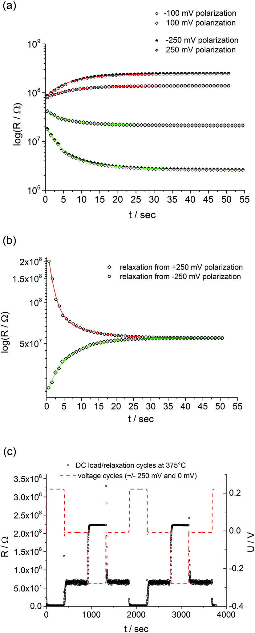 | ||
| Fig. 6 A finite time is required to reach a steady state resistance under an applied bias voltage. This is shown in (a) for a 150 nm STO film at 375 °C (Tset) and ±100 mV and ±250 mV, respectively. By switching off the voltage, a relaxation process takes place. In (b) the relaxation of the resistance probed by a small DC voltage (±5 mV) after polarization by ±250 mV at 375 °C (Tset) is shown. (c) Various cycles with positive and negative voltages show the reproducibility of the polarization and relaxation processes. | ||
Stoichiometry polarization with a voltage dependent steady state oxygen vacancy distribution, i.e. δ(x), also means that for each steady state value in the slow I–V curve the defect chemical situation in the SrTiO3−δ(x) film is different. For large voltages, strong and polarity dependent oxygen chemical potential gradients ∇μ(x) and thus ∇δ(x) should exist while for small voltages the sample is (almost) in equilibrium with the gas phase. In other words, at slow scan rates the I–V curve does not reflect a non-linearity of a static and homogeneous sample but is the result of a film with inhomogeneous properties and composition (δ(x)) which differs in each measurement point. This is sketched in Fig. 4: each voltage corresponds to a different defect chemical situation of the thin film; in the sketches, it is assumed that STO at the LSC electrode (left side of the sketch) is always in equilibrium with the gas phase.
Whenever one is interested in I–V characteristics of a fixed composition (either fixed δ(x) or ∇δ = 0), one has to measure so fast that within the measurement time the vacancy distribution cannot vary, i.e. with scan rates that do not allow any ion redistribution. Please note that this inability of ions (vacancies) to follow the voltage signal does not refer to the individual jumps of ions but to establishing a new long-range vacancy distribution in the entire film. Hence, distances of the order of the film thickness have to be considered. According to these considerations it is thus hardly surprising that fast I–V curves (probing a fixed δ(x), see sketch in Fig. 5a) differ from the slow ones (probing sample variations with voltage, see Fig. 4). It is also clear that fast curves must depend on the starting voltages, since those determine δ(x) (see Fig. 5b).
Hence, the existence of different fast and slow I–V curves is very realistic if not unavoidable in SrTiO3 films. Thus, also the appearance of inductive loops and additional arcs in impedance spectra is no longer surprising. The minimum scan rate required for fast I–V curves depends on the sample thickness and for macroscopic samples much slower scan rates are necessary for probing the I–V curves of the given δ(x) distributions. The corresponding impedance features (loop or additional arc) are expected at much lower frequencies and may easily run out of typically measured frequency ranges. This may be one of the reasons that, to the best of the authors’ knowledge, such effects have not been reported so far, despite many studies dealing with stoichiometry polarization.
4.2 Quantification of slow and fast I–V curves
It remains to be discussed why slow as well as fast I–V curves with a positive starting voltage are more or less exponential-like. When quantitatively analyzing the I–V curves, the specific defect chemical and transport properties of the thin films come into play and thus many unknown parameters. So far, we only know that the thin films strongly differ from macroscopic bulk samples and that the properties measured in this study are not mainly due to interfacial effects (e.g. space charges at the electrodes) but refer to the entire film, see section 3.1. Preliminary tracer diffusion experiments showed very low oxygen diffusion coefficients and probably the electronic conductivity is larger than the ionic one (σeon > σion). In other words, the measured AC as well as DC currents are mainly electronic (either from electron holes or from electrons).Similar to bulk STO we assume that oxygen vacancies are still the majority mobile defect, their small contribution to the current is then only due to their low mobility. Hence, we face a situation that corresponds to Wagner–Hebb-type stoichiometry polarization: one electrode blocks the majority charge carrier (Nb:STO) and the second electrode is reversible for both charge carriers (LSC). At the reversible electrode, the chemical potential of the corresponding component is fixed (here oxygen is fixed by the gas atmosphere). In such a case, the steady state current voltage curve (electronic current ieon due to holes ih and electrons ievs. voltage U) is given by35,51,52
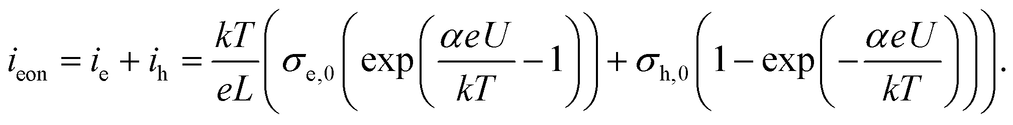 | (1) |
Symbols σe,0 and σh,0 denote the electron and electron hole conductivity for the chemical potential of the reversible electrode (i.e. gas phase), k, T, e, L are Boltzmann's constant, temperature, elementary charge and film thickness, respectively and for standard Wagner–Hebb polarization of an oxide the α value should be one.
We may now apply eqn (1) to quantify the measured slow I–V curves. Owing to the obvious absence of a significant exponential part for negative voltages, only the positive voltage part is considered and the second term in eqn (1) is neglected. A rather good agreement between fit and measured curve is found, see Fig. 7a. The α-value (0.93) is close to what we expect for ideal behavior (1.0). Hence, we consider it as highly probable that without bias, our film is either electron conducting (on a very low level) or close to the intrinsic minimum of electronic conductivity with little effect of ih for positive voltages. A film with almost intrinsic electron concentration would also be in accordance with preliminary p(O2) dependent measurements which showed little change of the conductivity between 1% and 100% O2 in the gas atmosphere. As already mentioned in section 3.1, this low charge carrier concentration despite Fe doping may be due to overlapping space charges caused by one-dimensional defects. The strongly hole conducting regime expected from eqn (1) for negative voltages seems to be absent here, possibly due to the very low oxygen vacancy concentration already existing without bias.
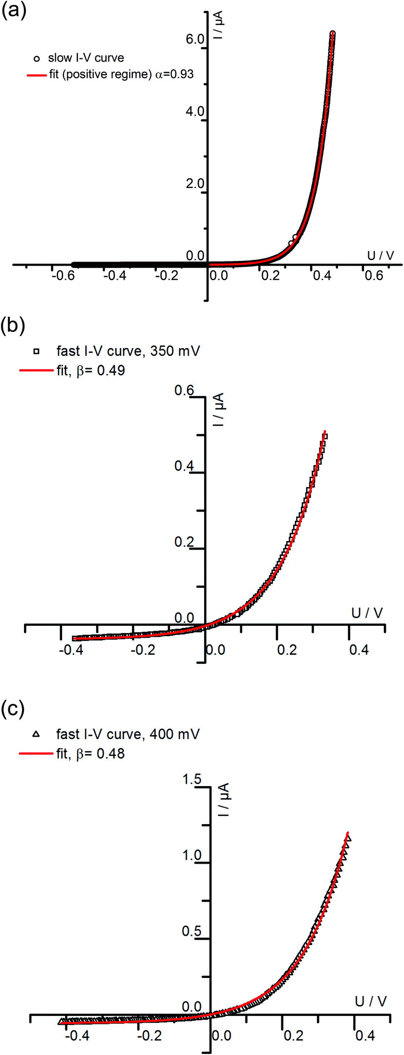 | ||
| Fig. 7 (a) The positive part of the slowly measured I–V curve for a 180 nm STO film conducted at 420 °C (Tset) is fitted using the first part of eqn (1). The resulting α of 0.93 is close to what is expected for ideal Wagner–Hebb behavior (α = 1). In (b) and (c) fast I–V curves of the same film and temperature starting at 350 mV (b) and 400 mV (c) were fitted by means of eqn (2). | ||
The fast I–V curve for positive starting voltage exhibits diode like behavior and therefore the diode equation
 | (2) |
4.3 Impedance model
Finally, we introduce a model not only to qualitatively understand the existence of inductive loops or second arcs in impedance measurements upon bias, but also to quantitatively fit the spectra and to interpret the corresponding capacitive and resistive contributions. This model is based on the assumption σeon ≫ σion, i.e. that ionic current does not directly contribute to a measurable current. Additional temperature dependent measurements on similar films (not shown here) suggest that such an assumption is valid in the temperature range between 450 °C and 750 °C. At lower temperatures, we cannot exclude that ionic conductivity needs to be considered, which may complicate the model but does not affect the main message.Despite this assumption of negligible ionic contribution to the overall current, ion flux is highly important since it leads to the build-up of the stoichiometry profile upon voltage load. At high frequencies, we can thus approximate the SrTiO3 thin film by a parallel RC element with resistance Rfast denoting the (differential) resistance of electron and hole current for a given δ(x) distribution in the film. The parallel capacitor Cgeo is the geometrical capacitance of the thin film which may be generalized by a constant phase element CPE with impedance ZCPE = (iω)−nQ−1. The capacitance C of such a R-CPE element can be estimated from53,54
 | (3) |
The measured resistance changes if the frequency comes into the range in which ions can move substantial distances within a single half wave of the AC sine function. Therefore, in each half wave of the AC signal novel charge carrier distributions develop within the thin film. At very low frequencies, ions can follow the AC voltage on the length scale of the sample thickness and alternatingly modify the already existing δ(x) (from DC polarization voltage) by Δδ(x). This is also illustrated in Fig. 8: on a time scale τδ after applying a DC voltage the ion blocking character of the Nb:STO leads to the formation of an oxygen vacancy distribution within the STO thin film; in Fig. 8a a linear profile is sketched for the sake of simplicity. Please note that the positive polarity on the LSC side does not indicate a shift of this thin film side to higher oxygen partial pressures, rather LSC pins the chemical potential of oxygen. Accordingly, at the LSC|Fe:STO interface a reversible exchange of all three charge carriers (electrons, holes and oxygen vacancies) is possible in contrast to the Nb:STO|Fe:STO interface where oxygen vacancies are blocked.
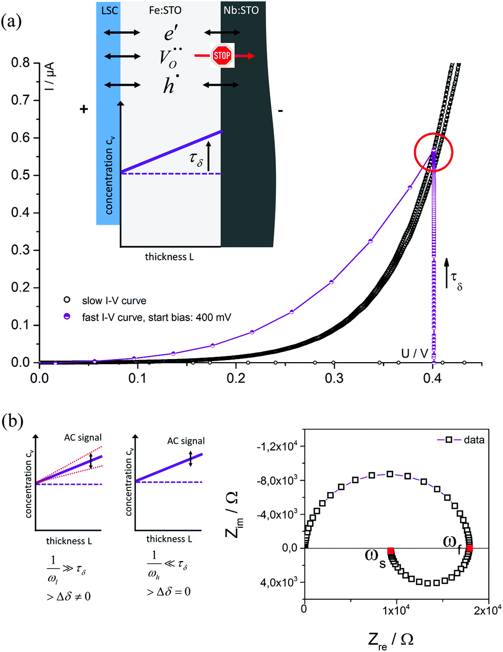 | ||
| Fig. 8 (a) A schematic sketch of the sample illustrates the build-up of an oxygen vacancy gradient under applied bias voltage (time constant τδ); for the sake of simplicity a linear profile is sketched. The concentration of ionic charge carriers is pinned at the LSC|Fe:STO interface but they can accumulate or deplete at the blocking Nb:STO|Fe:STO interface depending on the polarity of bias. (b) Impedance measurements upon bias probe slopes of I–V curves (as shown in a). The impedance spectra consist of two features at different frequencies. In the high frequency arc, ions cannot follow the AC voltage changes, i.e. the given vacancy distribution does not vary, Δδ = 0; the slope of the fast I–V curve is measured for ωf. At low frequencies (ωs) the ions redistribute according to the given AC amplitude and the slope of the slow I–V curve is detected. | ||
High probing frequencies ωf do not affect the corresponding stoichiometry profile (Δδ = 0); this refers to the intermediate frequency intercept of the impedance spectrum and to the slope of the fast I–V curve. For low frequencies ωs however, the concentration profile follows the voltage variation established either by AC (low frequency intercept in the spectrum) or by DC (slope of the slow I–V curve). Hence, we indeed get a finite Δδ(x). At low frequencies the film resistance Rslow probed by impedance therefore differs from the high frequency case (Rfast) and we get
| Rslow = Rfast + ΔRslow | (4) |
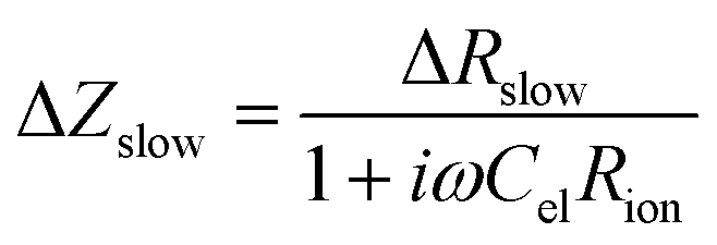
| ΔZslow = F(ω)·ΔRslow. | (5) |
 | ||
| Fig. 9 The frequency dependent changes of the sample stoichiometry under bias need to be included in the equivalent circuit. Therefore, an additional ΔZslow (a) is introduced, which includes a weight factor F(ω) that can be correlated with the stoichiometry changes; F(ω) is determined by the ionic rail, given by Rion and Cel (b). All these considerations lead to the final equivalent circuit in (c). | ||
Here, ion transport comes into play, since its kinetics determines whether or not the given stoichiometry distribution δ(x) is changed by the AC voltage. Hence, the time constant of the stoichiometry change via ion transport has to correlate with F(ω). The simplest way of representing ion transport in such a mixed conductor with one ion blocking electrode is by a serial connection of the ionic resistance Rion and an ion-blocking interfacial capacitance Cel. In general, the impedance of a mixed conductor also includes a chemical capacitance,55 and ion transport may have an additional contribution from the oxygen exchange kinetics at the quasi-reversible LSC electrode. The chemical capacitance is neglected here due to the small volume of the film; the area specific chemical capacitance can be approximated by  for electronic minority charge carrier concentration (ceon)56 and with L = 400 nm (film thickness) and ceon < 1016 cm−3, we obtain at 500 °C values <1 μF cm−2. The electrode kinetics of LSC is assumed to be fast compared to ion transport in SrTiO3, i.e. the oxygen chemical potential at the LSC|Fe:STO interface is pinned. Hence, a serial RionCel element is a realistic approximation of the ionic conduction in the film and the time constant of the stoichiometry polarization is given by τδ = RionCel. The weight factor F(ω) may then be defined by
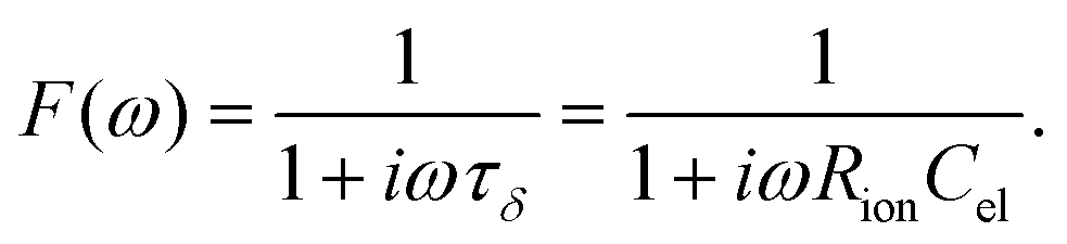 | (6) |
This F(ω) correctly describes the time (or frequency) dependence of Δδ(x): F(ω) = 0 (Δδ = 0) for high frequencies and F(ω) = 1, i.e. modification of δ(x) by Δδ for low frequencies (Fig. 9b).
Combining eqn (5) and (6) leads to
 | (7) |
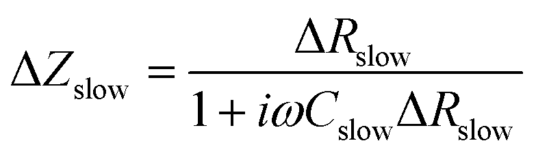 | (8) |
 | (9) |
Eqn (8) corresponds to a parallel RC element consisting of resistance ΔRslow and capacitance Cslow. Hence, we finally get the circuit given in Fig. 9c with ΔZslow corresponding to an RC element. However, both elements in ΔZslow have non-trivial meanings: ΔRslow was already discussed above and Cslow is even more complicated since it includes contributions of one conventional interfacial capacitance (Cel) and two resistances, one of them having a non-trivial meaning itself (ΔRslow). Since ΔRslow may be negative, also Cslow can exhibit negative values, which is not unphysical since it is not a simple electrostatic capacitance but a combined property of three sample features. Moreover, CPE elements rather than ideal capacitors are used in the fit circuit; a Cslow value was then calculated from CPEslow, Rslow and eqn (3).
Fig. 10a displays that the circuit excellently fits the spectra with inductive loops. Typical exponents n were in the range between 0.94 and 0.98 for both CPEgeo and CPEslow. Excellent fit agreement is also found for situations with an additional low frequency arc; i.e. for negative starting voltage. However, in those cases the high frequency part of the spectrum shows an additional splitting into two arcs and this is taken into account empirically by an additional serial R-CPE element (RHF − CPEHF), see Fig. 10b. Here, this high frequency modification is not further interpreted, only the results of the low frequency part are considered for the following analysis. Fig. 11a displays Arrhenius plots of Rfast (+RHF) of one sample for different bias values. Fig. 11c plots the temperature dependence of the absolute values of Cslow found in the same film for different bias voltages. Cslow shows a significant bias dependence and the values for +400 and −400 mV differ by more than one order of magnitude. The absolute value is in the range of a few mF cm−2 for 400 mV and thus higher than any realistic interfacial capacitance. Most striking, however, is the Arrhenius-type behavior of Cslow with an activation energy of around 0.5 eV.
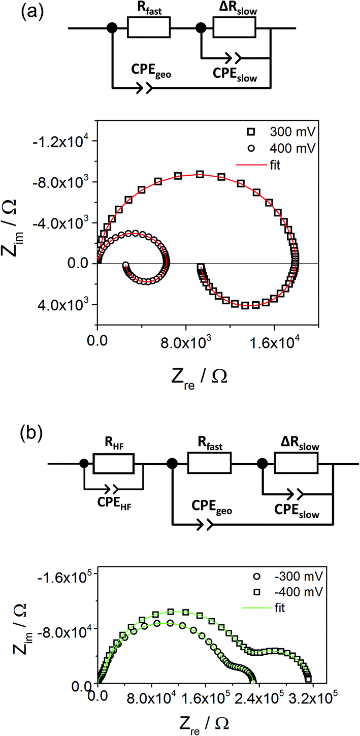 | ||
| Fig. 10 Low frequency loops for the 180 nm STO thin film at 625 °C (Tset) in the positive regime (a) as well as low frequency second semicircles in the negative regime (b) can be fitted quite accurately with the given equivalent circuits. An additional small arc in the high frequency range develops for the negative voltages. This is taken into account by another RHF − CPEHF element, but is not further discussed in this paper. | ||
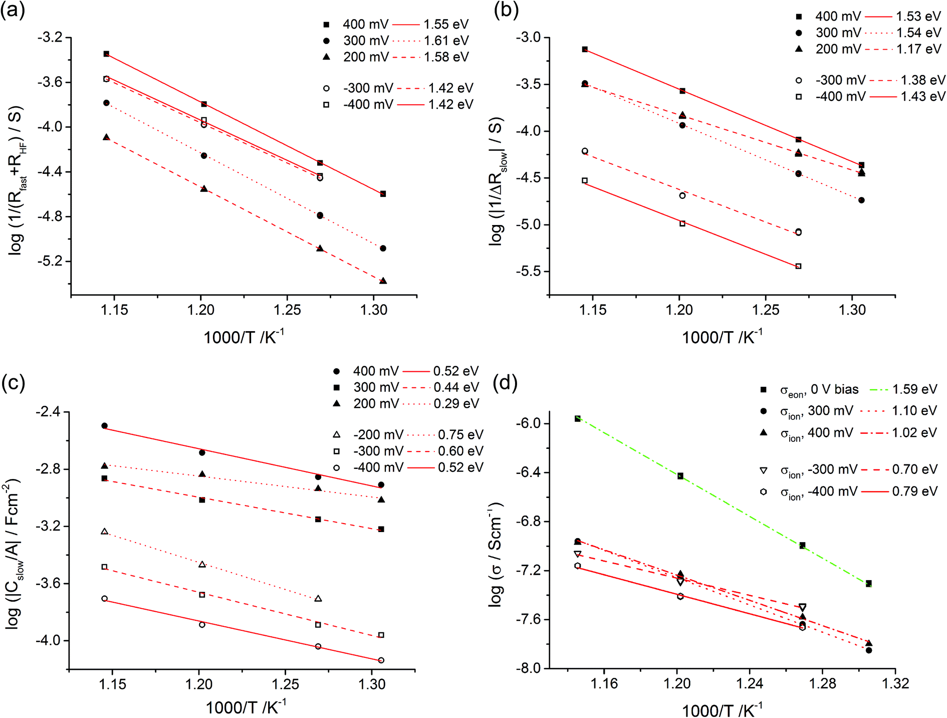 | ||
| Fig. 11 Temperature dependent parameters deduced from the equivalent circuit model for a 180 nm STO layer under different bias voltages. Arrhenius behavior of Rfast (+RHF) values (a) and of ΔRslow (b) with activation energies. In (c) the area-specific capacitance (Cslow/A) is plotted. (d) Estimation of the ionic conductivity using eqn (9) and Cel = 20 μF cm−2. For comparison, also the conductivity determined from high frequency arcs without bias (σeon) is shown. | ||
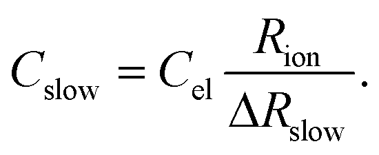
All these features of Cslow can be understood from our model i.e. from eqn (9). Since ΔRslow, δ(x) and thus also Rion depend on the polarity and voltage, a strong voltage dependence of Cslow is not surprising. As a first approximation we may assume a temperature and bias independent interfacial capacitance Cel. Then, the temperature dependence of Cslow is determined by the different temperature dependences of Rion and ΔRslow. The Arrhenius plots of 1/ΔRslow are given in Fig. 11b and reveal activation energies between 1.1 eV and 1.5 eV. Together with the measured activation energies of Cslow this suggests an activation energy of 0.7 eV–1.1 eV for Rion, a value range that is very realistic for oxygen vacancy conduction.
Based on this model, a further property can be deduced from our measurements: even though the ionic conductivity is most probably too low to significantly contribute to the measured STO thin film resistance in the given temperature range, it enters the equation of the measured capacitance Cslow. An exact value of the ion blocking interfacial capacitance is not available, but 20 μF cm−2 may serve as a reasonable first estimate; this corresponds to a relative permittivity of ca. 100 and a capacitor thickness of 4 nm. Based on this assumption we can estimate the ionic resistance by eqn (9) for each temperature and voltage and the resulting averaged ionic conductivity values are plotted in Fig. 11d. Not surprisingly, these values depend on bias since each voltage corresponds to a certain δ(x). Extrapolation of the values to 0 V could lead to the true ionic conductivity of the layer. Owing to the lack of sufficient data an exact interpolation is not possible in our case. However, the voltage dependence is not very pronounced anyway and, for example, we get σion = 1.1 × 10⁻⁷ S cm−1 at 600 °C. This is much smaller than σeon = 1.2 × 10⁻⁶ S cm−1 estimated from the high frequency semicircle of the 0 V measurements at the same temperature. Owing to different activation energies of σion and σeon, the values approach each other at lower temperatures and we get σion = 8.0 × 10⁻¹⁰ S cm−1 (400 mV bias measurement) and σeon = 7.6 × 10⁻¹⁰ S cm−1 for 400 °C (not shown in Fig. 11d).
This quantitative analysis of the bias dependent impedance measurements thus offers a novel tool for estimating ionic conductivities of thin films even if σion ≪ σeon hinders a straightforward measurement; it becomes accessible from Cslow and the measured ΔRslow. However, the proportionality to Cel leaves a significant uncertainty in this estimate.
From the consistency of all these considerations we conclude that the inductive loops or second arcs found in the impedance spectra of SrTiO3 films upon bias are a very clear trace of ion motion in these layers. Analogous effects are expected in many other oxide films or thin bulk layers. Moreover, the situation is only slightly changed when two ion blocking electrodes are used instead of one. The pinning of the composition at the reversible electrode is then no longer present but fast I–V curves again have to be different and loops and/or second arcs are again expected. The effects shown in this paper should thus be rather ubiquitous phenomena. The reason for not yet finding many reports on such effects may simply be the fact that inductive loops are often assumed to be measurement artefacts, and were often not further investigated so far.
5. Conclusion
Upon voltage load at elevated temperatures, stoichiometry polarization takes place in slightly Fe-doped SrTiO3 thin films deposited on ion blocking Nb-doped SrTiO3 substrates. During polarization the oxygen vacancy concentration changes until an inhomogeneous steady state distribution is reached. For slowly measured current voltage (I–V) curves, each measurement point thus corresponds to a different sample situation, i.e. a different oxygen vacancy profile in the film. The I–V curves measured for positive voltages at a reversible (La0.6Sr0.4)CoO3−δ top electrode are close to those expected from standard Wagner–Hebb theory with electrons in the oxide as the relevant electronic minority charge carriers. I–V curves measured with fast scan rates, however, depend on the starting voltage (steady state established prior to the measurement) and also differ from those predicted by Wagner–Hebb theory. This is due to the fact that for fast scan rates the SrTiO3 thin films do not change their vacancy distribution during the measurement. Accordingly, fast and slow I–V curves exhibit different slopes for one and the same voltage.This difference is reflected in an uncommon impedance feature of SrTiO3 thin films measured upon bias: inductive loops are often found at low frequencies and in some cases additional semicircles show up. These phenomena are nothing but the small signal AC equivalent of the scan rate dependent slopes of I–V curves. They are caused by the time required for oxygen vacancies to redistribute after a voltage change (bias or AC signal) and thus depend on the ionic resistance of the SrTiO3 thin film. In other words, the inductive loops (or additional arcs) measured upon bias are traces of ion motion in the films, even if the ionic current is negligible compared to the electronic one. An equivalent circuit model was derived, which not only fitted the spectra but could also explain the main features of the deduced parameters, including the negative sign of the corresponding capacitance, its high activation energy and its strong bias dependence. Based on an estimate of the interfacial capacitance at the ion blocking electrode, such measurements even constitute a novel method for obtaining information on the ionic conductivity of mixed conducting thin films with a very small ionic transference number. Similar effects are expected in many mixed conducting oxide thin films, provided the time constants of stoichiometry polarization get into the frequency range of impedance measurements.
Acknowledgements
The authors gratefully acknowledge funding by FWF (Austrian Science Fund) project F4509-N16. Furthermore, we would like to thank Prof. Gernot Friedbacher for conducting AFM measurements and Prof. Andreas Limbeck for performing ICP-MS measurements. TEM images were obtained using facilities at the University Service Centre for Transmission Electron Microscopy, Vienna University of Technology, Austria.References
- R. A. De Souza, J. Fleig, R. Merkle and J. Maier, Z. Metallkd., 2003, 94, 218–225 CrossRef CAS.
- R. Merkle, Phys. Chem. Chem. Phys., 2002, 4, 4140–4148 RSC.
- R. Merkle and J. Maier, Angew. Chem., Int. Ed., 2008, 47, 3874–3894 CrossRef CAS PubMed.
- R. Waser, J. Am. Ceram. Soc., 1991, 74, 1934–1940 CrossRef CAS.
- I. Denk, W. Muench and J. Maier, J. Am. Ceram. Soc., 1995, 78, 3265–3272 CrossRef CAS.
- F. Noll, W. Münch, I. Denk and J. Maier, Solid State Ionics, 1996, 86–88((Part 2), 711–717 CrossRef.
- M. Leonhardt, R. A. De Souza, J. Claus and J. Maier, J. Electrochem. Soc., 2002, 149, J19–J26 CrossRef CAS.
- R. A. De Souza, V. Metlenko, D. Park and T. E. Weirich, Phys. Rev. B: Condens. Matter, 2012, 85, 174109 CrossRef.
- R. Waser, Solid State Ionics, 1995, 75, 89–99 CrossRef CAS.
- X. Guo, J. Fleig and J. Maier, Solid State Ionics, 2002, 154–155, 563–569 CrossRef CAS.
- S. Rodewald, J. Fleig and J. Maier, J. Am. Ceram. Soc., 2001, 84, 521–530 CrossRef CAS.
- R. A. De Souza, J. Fleig and J. Maier, J. Am. Ceram. Soc., 2003, 86, 922–928 CrossRef CAS.
- R. A. De Souza, Phys. Chem. Chem. Phys., 2009, 11, 9939–9969 RSC.
- I. Denk, F. Noll and J. Maier, J. Am. Ceram. Soc., 1997, 80, 279–285 CrossRef CAS.
- R. Waser, T. Baiatu and K. H. Härdtl, J. Am. Ceram. Soc., 1990, 6, 1645–1653 CrossRef.
- S. Rodewald, N. Sakai, K. Yamaji, H. Yokokawa, J. Fleig and J. Maier, J. Electroceram., 2001, 7, 95–105 CAS.
- R. A. De Souza and M. Martin, Phys. Chem. Chem. Phys., 2008, 10, 2356–2367 RSC.
- P. Balaya, J. Jamnik, J. Fleig and J. Maier, Appl. Phys. Lett., 2006, 88, 062109–062103 CrossRef.
- P. Balaya, J. Jamnik, J. Fleig and J. Maier, J. Electrochem. Soc., 2007, 154, P69–P76 CrossRef CAS.
- G. Gregori, P. Lupetin and J. Maier, ECS Trans., 2012, 45, 19–24 CrossRef CAS.
- P. Lupetin, G. Gregori and J. Maier, Angew. Chem., Int. Ed., 2010, 49, 10123–10126 CrossRef CAS PubMed.
- M. Kubicek, Z. Cai, W. Ma, B. Yildiz, H. Hutter and J. Fleig, ACS Nano, 2013, 7, 3276–3286 CrossRef CAS PubMed.
- Z. Cai, Y. Kuru, J. W. Han, Y. Chen and B. Yildiz, J. Am. Chem. Soc., 2011, 133, 17696–17704 CrossRef CAS PubMed.
- H. Jalili, J. W. Han, Y. Kuru, Z. Cai and B. Yildiz, J. Phys. Chem. Lett., 2011, 2, 801–807 CrossRef CAS.
- C. Ohly, S. Hoffmann-Eifert, X. Guo, J. Schubert and R. Waser, J. Am. Ceram. Soc., 2006, 89, 2845–2852 CrossRef CAS.
- R. A. De Souza, F. Gunkel, S. Hoffmann-Eifert and R. Dittmann, Phys. Rev. B: Condens. Matter, 2014, 89, 2414011–2414015 CrossRef.
- T. Menke, P. Meuffels, R. Dittmann, K. Szot and R. Waser, J. Appl. Phys., 2009, 105, 066104 CrossRef.
- K. Szot, W. Speier, G. Bihlmayer and R. Waser, Nat. Mater., 2006, 5, 312–320 CrossRef CAS PubMed.
- R. Waser, R. Dittmann, C. Staikov and K. Szot, Adv. Mater., 2009, 21, 2632–2663 CrossRef CAS.
- R. Waser and M. Aono, Nat. Mater., 2007, 6, 833–840 CrossRef CAS PubMed.
- R. Dittmann, R. Muenstermann, I. Krug, D. Park, T. Menke, J. Mayer, A. Besmehn, F. Kronast, C. M. Schneider and R. Waser, Proc. IEEE, 2012, 100, 1979–1990 CrossRef CAS.
- R. Muenstermann, T. Menke, R. Dittmann and R. Waser, Adv. Mater., 2010, 22, 4819–4822 CrossRef CAS PubMed.
- C. Lenser, A. Koehl, I. Slipukhina, H. Du, M. Patt, V. Feyer, C. M. Schneider, M. Lezaic, R. Waser and R. Dittmann, Adv. Funct. Mater., 2015, 25, 6360–6368 CrossRef CAS.
- C. Lenser, M. Patt, S. Menzel, A. Köhl, C. Wiemann, C. M. Schneider, R. Waser and R. Dittmann, Adv. Funct. Mater., 2014, 24, 4466–4472 CrossRef CAS.
- C. Wagner, Proc. 7th Meeting of Int. Comm. on Electrochem. - Thermodynamics and Kinetics, 1955, p. 361.
- T. Baiatu, R. Waser and K. H. Härdtl, J. Am. Ceram. Soc., 1990, 6, 1663–1673 CrossRef.
- R. Waser, T. Baiatu and K. H. Härdtl, J. Am. Ceram. Soc., 1990, 6, 1654–1662 CrossRef.
- S. Rodewald, J. Fleig and J. Maier, J. Am. Ceram. Soc., 2000, 83, 1969–1976 CrossRef CAS.
- S. Rodewald, J. Fleig and J. Maier, J. Eur. Ceram. Soc., 1999, 19, 797–801 CrossRef CAS.
- M. Kubicek, A. Limbeck, T. Frömling, H. Hutter and J. Fleig, J. Electrochem. Soc., 2011, 158, B727–B734 CrossRef CAS.
- G. M. Rupp, A. Limbeck, M. Kubicek, A. Penn, M. Stoger-Pollach, G. Friedbacher and J. Fleig, J. Mater. Chem. A, 2014, 2, 7099–7108 CAS.
- A. V. Berenov, A. Atkinson, J. A. Kilner, E. Bucher and W. Sitte, Solid State Ionics, 2010, 181, 819–826 CrossRef CAS.
- E. Bucher, W. Jantscher, A. Benisek, W. Sitte, W. Preis, I. Rom and F. Hofer, Solid State Ionics, 2001, 141–142, 375–380 CrossRef CAS.
- T. M. Huber, A. K. Opitz, M. Kubicek, H. Hutter and J. Fleig, Solid State Ionics, 2014, 268(Part A), 82–93 CrossRef CAS.
- J. Jamnik, Solid State Ionics, 2006, 177, 2543–2547 CrossRef CAS.
- J. S. Lee, J. Fleig, J. Maier, T. J. Chung and D. Y. Kim, Solid State Ionics, 2005, 176, 1711–1716 CrossRef CAS.
- J. S. Lee, J. Fleig, J. Maier, D. Y. Kim and T. J. Chung, J. Am. Ceram. Soc., 2005, 88, 3067–3074 CrossRef CAS.
- J. Fleig, J. Jamnik, J. Maier and J. Ludvig, J. Electrochem. Soc., 1996, 143, 3636–3641 CrossRef CAS.
- R. Srinivasan, ECS Trans., 2011, 33, 21–35 Search PubMed.
- J. P. Diard, B. Le Gorrec and C. Montella, J. Electroanal. Chem., 1992, 326, 13–36 CrossRef CAS.
- X. Guo and J. Maier, Solid State Ionics, 2000, 130, 267–280 CrossRef CAS.
- I. Riess, Solid State Ionics, 1992, 51, 219–229 CrossRef CAS.
- G. J. Brug, A. L. G. van den Eeden, M. Sluyters-Rehbach and J. H. Sluyters, J. Electroanal. Chem. Interfacial Electrochem., 1984, 176, 275–295 CrossRef CAS.
- C. H. Hsu and F. Mansfeld, Corrosion, 2001, 57, 747–748 CrossRef CAS.
- J. Jamnik and J. Maier, J. Electrochem. Soc., 1999, 146, 4183–4188 CrossRef CAS.
- J. Jamnik and J. Maier, Phys. Chem. Chem. Phys., 2001, 3, 1668–1678 RSC.
| This journal is © The Royal Society of Chemistry 2016 |