
 Open Access Article
 This Open Access Article is licensed under a
 Creative Commons Attribution 3.0 Unported Licence
A gate-tunable single-molecule diode†
Mickael L.
Perrin
a,
Elena
Galán
b,
Rienk
Eelkema
b,
Joseph M.
Thijssen
a,
Ferdinand
Grozema
b and
Herre S. J.
van der Zant
*a
aKavli Institute of Nanoscience, Delft University of Technology, Lorentzweg 1, 2628 CJ Delft, The Netherlands. E-mail: H.S.J.vanderZant@tudelft.nl
bDepartment of Chemical Engineering, Delft University of Technology, Julianalaan 136, 2628 BL Delft, The Netherlands
First published on 6th April 2016
Abstract
In the pursuit of down-sizing electronic components, the ultimate limit is the use of single molecules as functional devices. The first theoretical proposal of such a device, predicted more than four decades ago, is the seminal Aviram–Ratner rectifier that exploits the orbital structure of the molecule. The experimental realization of single-molecule rectifiers, however, has proven to be challenging. In this work, we report on the experimental realization of a gate-tunable single-molecule rectifier with rectification ratios as high as 600. The rectification mechanism arises from the molecular structure and relies on the presence of two conjugated sites that are weakly coupled through a saturated linker. The observed gate dependence not only demonstrates tunability of the rectification ratio, it also shows that the proposed rectification mechanism based on the orbital structure is operative in the molecule.
The theoretical design of the first molecular rectifier marked the birth of the field of single-molecule electronics.1 Since that proposal, many other mechanisms leading to rectification have been explored.2–5 However, due to experimental limitations, it was not until 2005 that the first single-molecule rectifier was built,6 albeit with a modest rectification ratio (RR) of 10. Since then, many more realizations have been proposed and realized,7–13 some of them based on molecule intrinsic properties,6–9 others exploiting contact effects.10–13 Here, we report on single-molecule devices of which the rectification mechanism is built into the molecule, with rectification ratios reaching up to 600. This rectification ratio is the result of the molecular structure and not of asymmetries in the coupling to the electrodes. The design is based on an asymmetric molecule consisting of two similar conjugated parts that are weakly coupled through a non-conjugated bridge. The conductance through these molecules was measured by forming molecular junctions using the mechanically controllable break junction (MCBJ) technique.14–16 A unique feature of the MCBJ measurements presented here is the use of a third electrode that acts as a gate. Using this gate electrode, the alignment of the electronic levels that are responsible for transport with the Fermi energy of the electrodes are altered, leading to a tunable rectification ratio. Moreover, the dependence of the rectification ratio on the gate-voltage gives direct proof that the two-site rectification mechanism is operational the molecule.
1 Diode design
The molecule used in this work, DPE-2F, consists of two conjugated parts, connected by a saturated ethane bridge that breaks the conjugation, as shown in Fig. 1a. Asymmetry is introduced by two fluorine atoms that are located on one of the phenyl rings, both in the ortho position with respect to the ethane group. The molecule is substituted at both ends with thiol groups that act as anchoring units for coupling to metallic electrodes. Details about the synthesis of the molecule can be found elsewhere.17Fig. 1b presents the energy diagram of the molecule, with the energy of the fluorine-containing part lowered by the electron withdrawing character of the fluorine substituents. A similar idea has very recently been put forward by van Dyck and Ratner18 but in their case the asymmetry is introduced in the anchoring groups.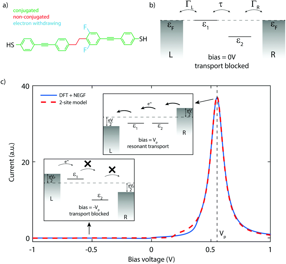 | ||
| Fig. 1 Molecule and diode mechanism. Chemical structure (a) of the DPE-2F molecule and its energy diagram (b), with the right half being lower in energy than the left one due to the electron withdrawing character of the fluorine substituents. (c) Current–voltage characteristic calculated using DFT + NEGF (solid blue, electronic coupling ΓL,R = 100 meV) and using the analytical expression for the two-site model (dashed red, electronic coupling ΓL,R = 25.8 meV.) The parameters ε1, ε2 and τ are obtained from the DFT calculations, and are equal to 0 meV, 299 meV and 11.9 meV, respectively. The voltage drop inside the molecule, α, is also obtained from DFT and is 0.54. The good agreement between the two calculated curves indicates that charge transport through the molecule can indeed be described using two sites, which form a delocalized bonding/anti-bonding HOMO/HOMO−1. Although in this calculation the peak is at positive bias, in the experiments, the orientation of the molecule cannot be controlled and therefore the peak in the current can be expected both at positive and negative bias voltages. | ||
Charge transport through the molecule can be understood from a two-site model,19 the use of which is supported by quantum chemistry calculations (see section I of the ESI† for a description of the model).20,21Fig. 1c shows a current–voltage (IV) characteristic (solid blue line) calculated for DPE-2F using density functional theory (DFT) combined with the non-equilibrium Green's function (NEGF) formalism (see section II of the ESI† for more details). As the energy of the sites is different at zero bias, the current is low. For positive bias, the sites are pulled towards each other and the current increases. At 0.55 V, a pronounced peak is visible. This is the point where the two sites have equal energy and resonant transport occurs. For higher voltages, the sites are pulled off resonance again and the current decreases. For reverse bias, conversely, the Stark shift causes the sites to be increasingly pulled apart. They therefore never align (see lower left panel of Fig. 1c) and the current remains low. Since current passes through the molecule only for a particular bias polarity, the molecule behaves as a rectifier. The figures of merit for a diode are the operating voltage (OP) and the rectification ratio (RR). As a definition for RR, we use the maximum ratio between the forward and reverse current determined at opposite bias polarities. For the calculated curve in Fig. 1c, this yields a RR of 751 and an operating voltage of 0.55 V.
2 Experimental
To investigate charge transport through single DPE-2F molecules, we employed the gateable mechanically controllable break junction (gMCBJ) technique,22–25 which is schematically depicted in Fig. 2a. The presence of the third electrode acting as a gate allows to tune the electrostatic potential of the molecule, thereby changing the alignment of the molecular levels responsible for transport with respect to the Fermi energy of the electrodes.26,27 To achieve this, the gate electrode needs to be located close to the molecule, but electrically insulated from the source/drain and the molecule.28 In our implementation, a aluminum gate is lithographically defined on top of a flexible phosporbronze substrate, electrically isolated from each other by a polyimide layer. After atomic-layer-deposition enhancement of the native gate oxide (Al2O3), a 15 nm thick gold wire is patterned on top of it. Finally, using an isotropic plasma etch, a free-standing gate/gate oxide/source–drain sandwich is formed. Fig. 2b and c present scanning electron micrographs of a gMCBJ device, in which the suspended sandwich is clearly visible. For more details about the fabrication and the characterization of the devices, we refer to sections VI–VII of the ESI.†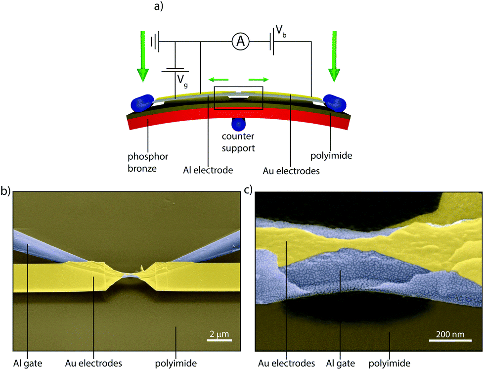 | ||
| Fig. 2 MCBJ technique with gate. (a) Schematic representation of the gMCBJ principle. (b, c) Scanning electron micrographs of a gMCBJ sample. | ||
The measurements are performed as follows. The molecular solution (0.1 mM in dichloromethane) is drop casted at room temperature on the unbroken electrodes, which are mounted in a three-point bending mechanism set-up. The set-up is pumped to high vacuum (≈1 × 10⁻⁶ mbar) and cooled down to 6 K by submersion in liquid helium. At base temperature, upon bending the substrate, the thin gold bridge is stretched until it breaks, after which two atomically sharp electrodes are formed.29 During the breaking, a molecule can be ‘trapped’ between these two electrodes and electrically characterized.15
3 Results
Fig. 3 presents measurements performed on two different gMCBJ devices. In Fig. 3a, a current–voltage characteristic (IV) recorded on sample 1 and at zero gate voltage is shown. The IV is highly asymmetric, with a peak in the current around 1.2 V. From this plot, we obtain a RR of 424, with a forward current of 1.7 nA, while the reverse current is only 4.04 pA (i.e., the current taken at −1.2 V). The inset shows IVs recorded at three different gate voltages. The current peak at positive bias, as well as the onset of the current, shift outward for increasingly positive gate voltage. This becomes more evident from Fig. 3b, where the differential conductance (dI/dV) is color coded as a function of bias and gate voltages. In the following we will refer to this kind of plot as a stability diagram. The color map shows a bright resonance which moves towards higher bias for higher positive gate voltage. The blue region represents the negative differential conductance (NDC). Altogether, all features shift towards higher bias for increasingly positive gate voltage, with a gate coupling of 7.5 mV V−1. This indicates HOMO-dominated charge transport.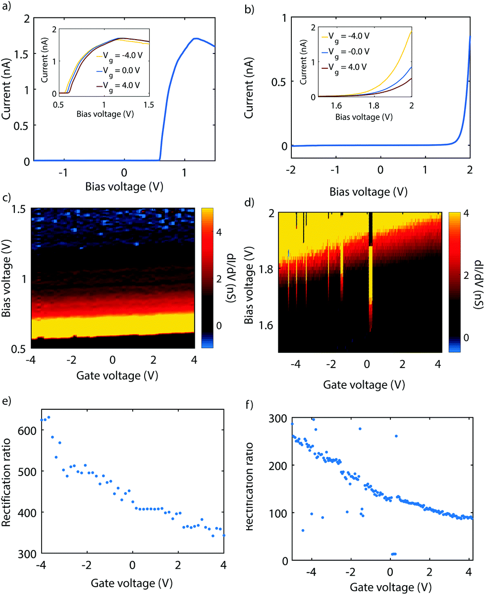 | ||
| Fig. 3 Gate tunability of the diode. Measurements recorded on sample 1 (a–c) and sample 2 (d–f). (a, d) Current–voltage characteristics recorded for various gate voltages. The inset shows a zoom-in on the reverse bias regime. (b, e) Color-coded map of the current as a function of bias and gate voltage. (c, f) Influence of gate voltage on the rectification ratio. | ||
Fig. 3c presents the rectification ratio as a function of gate voltage. It reaches its highest value (RR = 620) for a gate voltage of −4 V and monotoneously decreases for increasingly more positive gate voltage, with a lowest value of 340 at 4 V. Fig. 3d shows an IV recorded at zero gate voltage on a different junction. Again, the IV is highly asymmetric. In contrast to Fig. 3a, no peak in the current is reached within the applied bias window. The RR is therefore calculated for the maximum bias voltage, yielding 130. Upon application of a gate voltage (see inset), the onset of current shifts towards higher bias voltages. In Fig. 3e, the corresponding stability diagram is shown. From the plot we extract a gate coupling of 20.5 mV V−1, and infer that transport is dominated by the HOMO. Fig. 3f presents the evolution of the RR with gate. As mentioned before, RR is 130 at zero gate voltage, but increases to about 260 when bringing the HOMO closer to the Fermi energy with a gate voltage of −5 V. For a gate voltage of 4 V, the RR is about 90, a factor of almost three lower.
4 Discussion
In total seven three-terminal junctions have been studied. All gated samples show HOMO-mediated transport and an increase in RR when a negative gate voltage is applied (and conversely a decrease in RR for positive gate voltages). The observation of HOMO-mediated transport is consistent with DFT calculations.20,21 The change in the RR can be understood considering the change in level alignment induced by the gate. As previously shown,20 the RR is the largest when the HOMO is on resonance with the Fermi energy, and decreases for an increasing level misalignment. When the sites are not on resonance with the Fermi energy, an increase of the HOMO energy is thus predicted to increase the RR. This trend is illustrated in the left panel of Fig. 4, in which the RR is plotted as a function of level alignment, as obtained from DFT + NEGF calculations. Applying a negative voltage on the gate moves the HOMO up, towards the Fermi energy, thereby increasing the RR, in agreement with our measurements.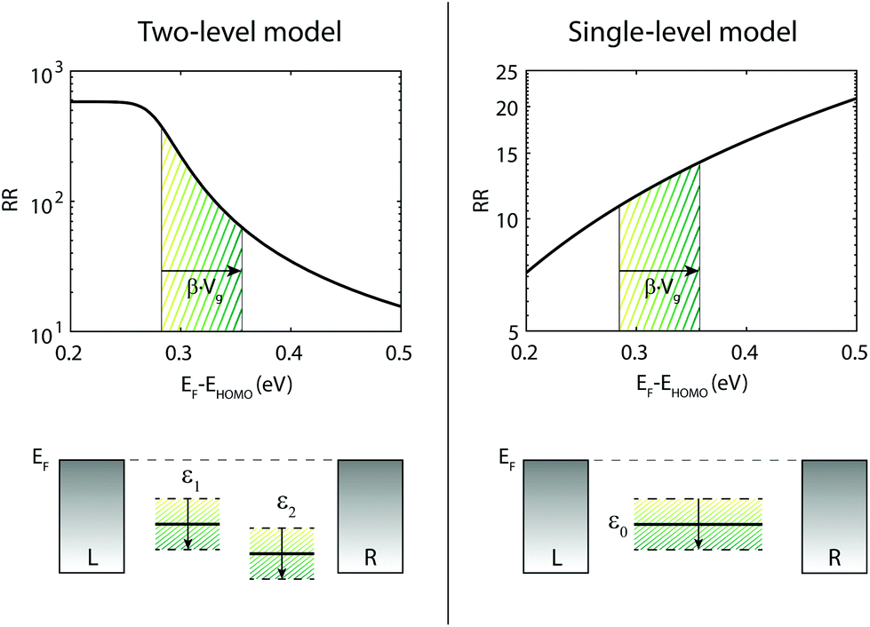 | ||
| Fig. 4 Influence of level alignment on the RR for single versus two site model. The top left panel shows the RR as a function of level alignment as calculated for the two-site model. As obtained in Fig. 1, we used in the model the following parameters: τ = 11.9 meV, α = 0.54 and ΓL,R = 25.8 meV. The bottom left panel shows the effect of the gate on the two sites. The top right panel depicts the RR as a function of gate for a single site. For this plot the used ΓL = 1 meV and ΓR = 100 meV. The RR increases for increasing level misalignment. This trend holds for various asymmetries in coupling. The bottom right plot illustrates the shift of the single site with gate. | ||
We investigated seven three-terminal samples, of which two are shown in the main text. In these two samples, we found HOMO-mediated transport and a RR of about 350–600 around 1.2 V for sample 1 and 100–260 around 1.9 V for sample 2. For the remaining samples we found HOMO-mediated transport as well and a gate tunability of the RR of 7–10 around −2.0 V for sample 3, 25–30 around 2.0 V for sample 4, 8–16 around 2.5 V for sample 5, 80–120 around 2.0 V for sample 6 and 80–110 around −1.1 V for sample 7. In addition, we measured thousands of two-terminal samples, of which the statistics can be found in section VIII of the ESI.†
We emphasize that the gate tunability of the RR is opposite to that expected for a molecular junction with asymmetrical electronic coupling in which transport is dominated by a single HOMO level close to the Fermi energy. In that case, the RR increases when the level is pulled away from the Fermi energy, as shown in the right panel of Fig. 4 and described in more detail in section V of the ESI.† In section IV of the ESI,† we demonstrate that this opposite trend is seen for a large range of electronic couplings, even for asymmetries in the electronic coupling up to a factor 100. In addition to rectification arising from molecule intrinsic properties, an asymmetry in the electronic coupling with the electrodes can further enhance the RR or reduce it, depending on whether fluorine containing halve is more strongly or weakly coupled.20 Nevertheless, the gate tunability in our junctions shows that the rectification mechanism originates from the molecular structure; an asymmetry in the electronic coupling merely modulates RR. It is the use of the gate electrode which allows for discriminating between the opposite behavior of a single- and a two-site system.
Another striking difference between the single- and two-level model is the presence of NDC in the latter case. The IVs shown in Fig. 3a exhibit NDC, a feature which cannot be explained using a single level only. In section VIII of the ESI,† we present several more IVs exhibiting distinct NDC.
It is also important to note that the diode performs optimally when the HOMO is close (<0.25 eV) to the Fermi energy. Taking the HOMO around 0.5 eV below the Fermi energy,30,31 our calculations yield a moderate RR ratio of around 15 for a symmetric coupling to the electrodes. However, the level alignment in experiments is not fixed and varies from junction to junction19,25,31 due to changes in the molecular conformation/anchoring and the possible formation of image-charges. Level shifts up to ±0.1–0.2 eV can occur, and it is these shifts that may bring HOMO closer to the Fermi energy (or further away) and improve (deteriorate) diode performance. As Fig. 4 shows, the level shifts (which have the same effect as a change in the gate voltage) induce corresponding shifts in the RR, which subsequently varies from around 500 to 10. Therefore, robust diode behaviour with a high RR thus not only requires an asymmetry in the energies of the two halves of the molecule, but also a favourable alignment with the Fermi energy of the leads.
We finally note that we also recorded IVs on junctions exposed to the symmetric DPE, as a reference. This molecule has the same molecular backbone as DPE-2F, but without the fluorine substituents. For this molecule, we do not observe the very high RR's observed for DPE-2F. Instead, the molecule exhibits NDC, symmetrically located in bias, as expected for this molecule (see ESI† section III). Upon application of a positive gate voltage, the NDC features shifts towards higher bias voltage. These trends agree with HOMO-mediated transport and the fact that the molecule can be described using two sites, which, in contrast to the asymmetric DPE-2F molecule, are aligned with each other at zero bias.19
5 Conclusions
In conclusion, we have designed and characterized a single-molecule rectifier that operates by a mechanism that is explicitly programmed into the molecular structure. Measurements using the gMCBJ technique show that rectification ratios higher than 600 can be reached with this new design. By employing a gate electrode, we have established that the rectification mechanism that is proposed on basis of electronic structure calculation is indeed occurring. Our findings show that specific electronic functionality can thus be implemented in single molecules by optimizing the internal molecular structure. One could furthermore envision a new class of molecular devices with more than two sites in series. With control over the electrostatic energy of the individual sites by the use of gates, this would allow for the realization of functional devices with no inorganic semiconducting counterpart, in which, for instance, one of the gate terminals is used to transit from negative differential conductance behavior to rectification.Acknowledgements
This research was carried out with financial support from the Dutch Foundation for Fundamental Research on Matter (FOM), the Dutch Organisation for Scientific Research (NWO), the Ministry of Education, Culture and Science (OCW), and by an ERC advanced grant (Mols@Mols). The authors would like to thank Prof. Dr Diana Dulić for careful reading of the manuscript and Max Koole for help with the fabrication of the three-terminal samples.References
- A. Aviram and M. A. Ratner, Chem. Phys. Lett., 1974, 29, 277–283 CrossRef CAS.
- P. E. Kornilovitch, A. M. Bratkovsky and R. Stanley Williams, Phys. Rev. B: Condens. Matter, 2002, 66, 165436 CrossRef.
- J. Taylor, M. Brandbyge and K. Stokbro, Phys. Rev. Lett., 2002, 89, 138301 CrossRef PubMed.
- M. Paulsson, F. Zahid and S. Datta, Handbook of Nanoscience, Engineering, and Technology, 2003 Search PubMed.
- R. M. Metzger, Chem. Rev., 2003, 103, 3803–3834 CrossRef CAS PubMed.
- M. Elbing, R. Ochs, M. Koentopp, M. Fischer, C. von Hanisch, F. Weigend, F. Evers, H. B. Weber and M. Mayor, Proc. Natl. Acad. Sci. U. S. A., 2005, 102, 8815–8820 CrossRef CAS PubMed.
- I. Diez-Perez, J. Hihath, Y. Lee, L. Yu, L. Adamska, M. A. Kozhushner, I. I. Oleynik and N. Tao, Nat. Chem., 2009, 1, 635–641 CrossRef CAS PubMed.
- J. Hihath, C. Bruot, H. Nakamura, Y. Asai, I. Diez-Perez, Y. Lee, L. Yu and N. Tao, ACS Nano, 2011, 5, 8331–8339 CrossRef CAS PubMed.
- E. Lörtscher, B. Gotsmann, Y. Lee, L. Yu, C. Rettner and H. Riel, ACS Nano, 2012, 6, 4931–4939 CrossRef PubMed.
- A. Batra, P. Darancet, Q. Chen, J. S. Meisner, J. R. Widawsky, J. B. Neaton, C. Nuckolls and L. Venkataraman, Nano Lett., 2013, 13, 6233–6237 CrossRef CAS PubMed.
- T. Kim, Z. F. Liu, C. Lee, J. Neaton and L. Venkataraman, Proc. Natl. Acad. Sci. U. S. A., 2014, 111, 10928–10932 CrossRef CAS PubMed.
- A. Batra, J. S. Meisner, P. Darancet, Q. Chen, C. Steigerwald, M. L. Nuckolls and L. Venkataraman, Faraday Discuss., 2014, 174, 79–89 CAS.
- B. Capozzi, J. Xia, O. Adak, E. J. Dell, Z.-F. Liu, J. C. Taylor, J. B. Neaton, L. M. Campos and L. Venkataraman, Nat. Nanotechnol., 2015, 10, 522–527 CrossRef CAS PubMed.
- J. M. Krans, J. M. van Ruitenbeek, V. V. Fisun, I. Y. Yanson and L. J. de Jongh, Nature, 1995, 375, 767–769 CrossRef CAS.
- M. A. Reed, C. Zhou, C. J. Muller, T. P. Buring and J. M. Tour, Science, 1997, 278, 252–254 CrossRef CAS.
- E. Scheer, N. Agraït, J. C. Cuevas, A. Levy Yeyati, B. Ludoph, A. Martín-Rodero, G. Rubio Bollinger, J. M. van Ruitenbeek and C. Urbina, Nature, 1998, 394, 154–157 CrossRef CAS.
- E. Galán, M. L. Perrin, F. Grozema, H. S. J. van der Zant and R. Eelkema, Org. Biomol. Chem., 2016, 14, 2439–2443 Search PubMed.
- C. Van Dyck and M. A. Ratner, Nano Lett., 2015, 15, 1577–1584 CrossRef CAS PubMed.
- M. L. Perrin, R. Frisenda, M. Koole, J. S. Seldenthuis, J. A. Celis Gil, H. Valkenier, J. C. Hummelen, N. Renaud, F. C. Grozema, J. M. Thijssen, D. Dulić and H. S. J. van der Zant, Nat. Nanotechnol., 2014, 9, 830–834 CrossRef CAS PubMed.
- M. L. Perrin, E. Galan, R. Eelkema, F. C. Grozema, J. M. Thijssen and H. S. J. van der Zant, J. Phys. Chem. C, 2015, 119, 5697–5702 CAS.
- M. Kilgour and D. Segal, J. Phys. Chem. C, 2015, 119, 25291–25297 CAS.
- A. R. Champagne, A. N. Pasupathy and D. C. Ralph, Nano Lett., 2005, 5, 305–308 CrossRef CAS PubMed.
- C. A. Martin, J. M. van Ruitenbeek and H. S. J. van der Zant, Nanotechnology, 2010, 21, 265201 CrossRef PubMed.
- S. Ballmann and H. B. Weber, New J. Phys., 2012, 14, 123028 CrossRef.
- M. L. Perrin, C. O. Verzijl, C. A. Martin, A. J. Shaikh, R. Eelkema, J. H. van Esch, J. M. van Ruitenbeek, J. M. Thijssen, H. S. J. van der Zant and D. Dulić, Nat. Nanotechnol., 2013, 8, 282–287 CrossRef CAS PubMed.
- K. Moth-Poulsen and T. Bjornholm, Nat. Nanotechnol., 2009, 4, 551 CrossRef CAS PubMed.
- H. Song, K. Youngsang, J. Y. Hee, J. Heejun, L. Reed and M. A. Takhee, Nature, 2009, 462, 1039 CrossRef CAS PubMed.
- M. L. Perrin, E. Burzurí and H. S. J. van der Zant, Chem. Soc. Rev., 2015, 44, 902–919 RSC.
- J. M. van Ruitenbeek, A. Alvarez, I. Piñeyro, C. Grahmann, P. Joyez, M. H. Devoret, D. Esteve and C. Urbina, Rev. Sci. Instrum., 1996, 67, 108–111 CrossRef CAS.
- B. Kim, S. H. Choi, X.-Y. Zhu and C. D. Frisbie, J. Am. Chem. Soc., 2011, 133, 19864–19877 CrossRef CAS PubMed.
- R. Frisenda, M. L. Perrin, H. Valkenier, J. C. Hummelen and H. S. J. van der Zant, Phys. Status Solidi B, 2013, 250, 2431–2436 CrossRef CAS.
Footnote |
| † Electronic supplementary information (ESI) available: DFT calculations on the DPE molecule, three-terminal measurements on the DPE molecule, additional analysis of the single-level model, three-terminal device fabrication scheme and device characterisation, and junction statistics. See DOI: 10.1039/C6NR00735J |
| This journal is © The Royal Society of Chemistry 2016 |