
 Open Access Article
 This Open Access Article is licensed under a
 Creative Commons Attribution 3.0 Unported Licence
Kinetic factors determining conducting filament formation in solid polymer electrolyte based planar devices†
Karthik
Krishnan
*,
Masakazu
Aono
and
Tohru
Tsuruoka
*
International Center for Materials Nanoarchitectonics (MANA), National Institute for Materials Science, 1-1 Namiki, Tsukuba 305-0044, Japan. E-mail: KRISHNAN.Karthik@nims.go.jp; TSURUOKA.Tohru@nims.go.jp
First published on 8th April 2016
Abstract
Resistive switching characteristics and conducting filament formation dynamics in solid polymer electrolyte (SPE) based planar-type atomic switches, with opposing active Ag and inert Pt electrodes, have been investigated by optimizing the device configuration and experimental parameters such as the gap distance between the electrodes, the salt inclusion in the polymer matrix, and the compliance current applied in current–voltage measurements. The high ionic conductivities of SPE enabled us to make scanning electron microscopy observations of the filament formation processes in the sub-micrometer to micrometer ranges. It was found that switching behaviour and filament growth morphology depend strongly on several kinetic factors, such as the redox reaction rate at the electrode–polymer interfaces, ion mobility in the polymer matrix, electric field strength, and the reduction sites for precipitation. Different filament formations, resulting from unidirectional and dendritic growth behaviours, can be controlled by tuning specified parameters, which in turn improves the stability and performance of SPE-based devices.
Introduction
The resistive switching phenomena that emerge in simple metal/ionic conductor/metal (MIM) structures play a key role in the development of future nonvolatile memory, neuromorphic device technologies, and so on.1–5 In general, resistive switching in a thin film comprised of inorganic and organic ion conducting materials is a promising approach in the development of atomic scale memory devices, such as atomic switches, where both binary logic states and quantized conductance states can be realized by the formation and dissolution of a conducting metal filament.6–8 The operation of such devices is based on the oxidation at an electrochemically active electrode (usually, Ag or Cu) interface, the subsequent migration of oxidized cations in the ion conducting medium, and finally the reduction of cations at the inert metal electrode (for instance, Pt or Au) interface to form a metal filament between the electrodes under electrical bias. However, filament formation takes place randomly as stochastic events, which limits the performance and stability of the device. Therefore, it is important to understand the key factors that control filament growth behaviour during resistive switching in such structures.Several attempts have been made to study filament growth processes in MIM structures microscopically using scanning probe microscopy9 and transmission electron microscopy10–12 (TEM) techniques. These studies, which focused mainly on inorganic oxide based devices, revealed that in some cases filament growth initiates from the active electrode, which is completely opposite to what occurs in the standard electrochemical metallization (ECM) model.13,14 This contrary behaviour was explained by differences in the redox rates at the interfaces and in ion mobility inside the insulating material.15 Recently, the bipolar electrode behaviour of metal clusters in dielectric films was also observed.15,16 In contrast to inorganic materials, few studies have been reported on filament growth behaviour in MIM devices that use organic materials such as polyfluorene derivative polymers17 and conducting polymers as the hole transport layer of field effect transistors.18
In recent years, we have demonstrated that an atomic switch can be realized using a solid polymer electrolyte (SPE) as the organic ion conducting medium.19–21 Because MIM structures have a film of Ag-salt incorporated polyethylene oxide (Ag–PEO) sandwiched between Ag and Pt electrodes, they exhibit stable resistive switching behaviour under sweeping of a bias voltage. PEO is considered to be an essential ion conducting electrolyte for atomic switch operations due to its high mechanical flexibility, good film forming ability and compatibility with various substrates.22–25 The enhanced ionic conductivity occurs preferentially in an amorphous region of PEO. Addition of Ag salt in the PEO matrix mostly influences the local relaxation and segmental motion of PEO chains to create free volume into which the ions migrate effectively.26,27 Very recently, successful in situ optical microscopy and ex situ scanning electron microscopy (SEM) observations were made of conducting filament growth behaviour in a planar structure, in which Ag (or Pt) and Pt electrodes were opposed with a gap distance ranging from 5 to 8 μm.28 The observation of this planar device enabled us to investigate how redox reactions and subsequent filament formations take place in the MIM structure. However, because of the larger gap distance (>5 μm), which is determined by photolithography processes, the device showed no repeatable switching behaviour even after the forming process was clearly observed.29 This indicates that planar devices with more confined configurations are required to correlate the filament growth process to switching behaviour.
In this study, we used electron-beam (EB) lithography processes to fabricated PEO-based planar devices with gap distances between electrodes ranging from ∼2 μm to ∼0.5 μm. Owing to these smaller gap distances, stable resistive switching behaviour can be observed up to 102 cycles in current–voltage (I–V) measurements. Subsequent SEM observations enabled us to investigate how filament growth processes are correlated with switching characteristics and how they are affected by the device configuration and experimental parameters such as gap distance, salt inclusion in the matrix, and the applied compliance current. From the results obtained, we discuss how switching behaviour is controlled by kinetic factors, which determine the filament formation processes in SPE-based atomic switches.
Experimental
Device fabrication
Ag/PEO/Pt and Ag/Ag–PEO/Pt planar devices were fabricated on an Si substrate covered with SiO2 (thickness of 300 nm). The 18 × 18 mm2 substrates were initially cleaned with acetone, 2-propanol, and distilled water with a 15 min ultra-sonication. Plasma ashing (Yamato Scientific Co., Ltd, Japan, PR 300) was performed for 5 min under an oxygen atmosphere to remove the remaining contaminant species from the substrate. Then, opposed 100 nm thick Pt and Ag electrodes were formed on the substrate by two cycles of EB lithography, followed by a lift-off process. The gap distance between the two electrodes was varied from ∼2, ∼1, to ∼0.5 μm. A 10 nm thick layer of Ti was inserted between the electrodes and the substrate as the adhesion layer. To compensate for position misalignment between the two electrodes in the lithography processes, the Pt electrode was made wider than that of the Ag electrode. After that, either a self-assembled PEO or an Ag–PEO film, with a thickness of ∼200 nm, was formed on the electrodes using a spin coating method. Finally, unnecessary areas of the film were wiped away to isolate the respective device. A schematic of the structure of the fabricated device is shown in Fig. 1a.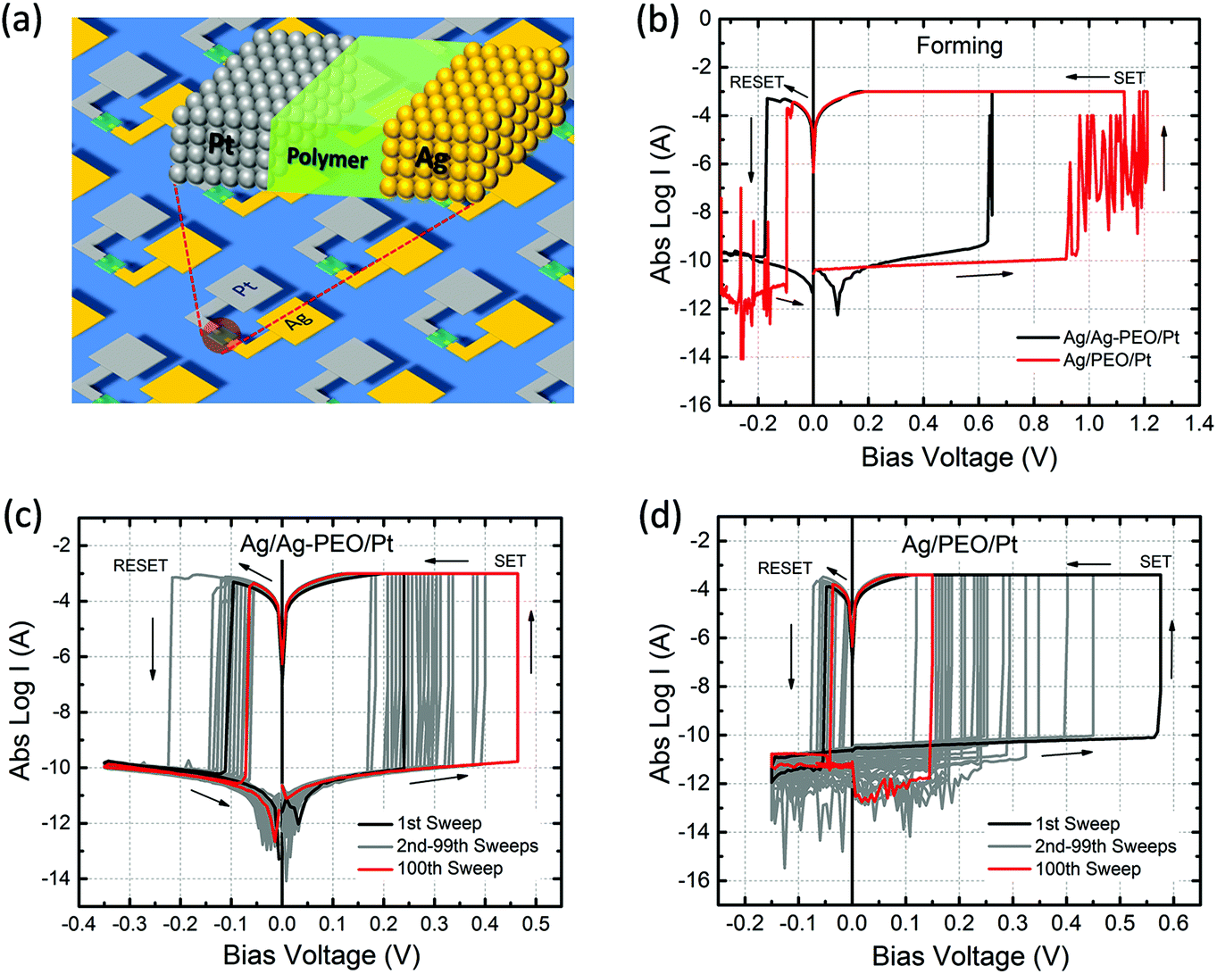 | ||
| Fig. 1 (a) Schematic of the fabricated planar device, (b) I–V plots for the initial forming process (with ICC = 1 mA) and the subsequent switching characteristics of both (c) Ag/Ag–PEO/Pt and (d) Ag/PEO/Pt planar devices measured for 100 consecutive sweeps (with a 5 s delay between each sweep). ICC was set at 1 mA and 400 μA for the Ag–PEO and PEO devices, respectively, for the switching cycles. | ||
PEO with a molecular weight of 5 × 10⁵ g mol−1 was used for the film preparation; to achieve a homogeneous solution, 0.1 g of PEO was initially dissolved in acetonitrile solvent (9.0 ml) and constantly stirred for 1 h at room temperature. Then, 150 μL of homogeneous PEO solution was used for spin coating (Active ACT-300D II/AII spin coater, Japan) to obtain a self-assembled structure on the substrate with the pre-fabricated electrodes. The Ag–PEO based device was fabricated in the same way, except that Ag-salt was added to the PEO solution while stirring. In the present study, 3 wt% of silver perchlorate (AgClO4) salt was used with 0.1 g of PEO.
Characterization
The I–V measurements of the fabricated planar devices were performed in air at room temperature using a semiconductor characterization system (Keithley 4200-SCS/F). A bias voltage was applied to the active Ag electrode and swept at a constant voltage sweep rate of 10 mV s−1, while the opposed inert Pt electrode was grounded. A certain compliance current (ICC) was fixed at positive bias to regulate the low-resistance (ON) state current, but no ICC was set for negative bias to turn the devices off (RESET) completely. The morphology of the filament growth between the electrodes was observed by SEM (Hitachi FE-SEM S-4800) after the I–V measurements.Results and discussion
Resistive switching characteristics
Fig. 1b shows typical I–V curves for Ag/Ag–PEO/Pt (black curve) and Ag/PEO/Pt (red curve) planar devices, measured at the first sweep cycle with an ICC of 1 mA. The gap distance was ∼1 and ∼0.5 μm for the Ag–PEO and PEO devices, respectively. Both devices exhibited a SET process from a pristine high-resistance (OFF) state to the ON state at positive bias. This first SET process corresponds to a forming process in which a metallic conducting filament is formed between the electrodes. The forming voltage was always lower for the Ag–PEO device than for the PEO device, as observed at ∼0.6 and ∼1.2 V respectively. The variation of this forming voltage between the two devices can be explained by the difference in concentrations and conductivities of Ag+ ions in their polymer matrixes. Ag–PEO devices, in which Ag+ ions pre-exist in the matrix, have higher ionic conductivities in their mixed crystalline and amorphous phases. Under positive bias, Ag+ ions oxidized from the Ag electrode and pre-dissolved Ag+ ions in the PEO matrix both migrate quickly toward the Pt electrode and contribute to the filament formation, resulting in the lower forming voltage. In contrast, in PEO devices, the absence of Ag+ ions in the pure PEO matrix results in a lowered ionic conductivity in the highly crystalline PEO. Therefore, large numbers of Ag+ ions are required to be injected into the PEO matrix for the first formation of a metal filament and they migrate slowly through the matrix, giving rise to the higher forming voltage. Under the subsequent negative bias, both devices were RESET from the ON state to the OFF state between −0.1 and −0.2 V. Note that the Ag/PEO/Pt device showed large current (spike-like) fluctuations before the forming and after the RESET process, as indicated by the red curve. These fluctuations, which were observed for the first few sweep cycles, are attributed to the structural instability of the metal filament in the pure PEO matrix during the initial formation and dissolution.The switching behaviour depends strongly on the gap distance between the electrodes and the applied ICC. We found that there is a critical limit for the gap distance value so as to achieve repeatable resistive switching characteristics. Fig. 1 represents the results of two devices with the limit value showing stable switching behaviour (∼1 μm for the Ag–PEO device and ∼0.5 μm for the PEO device). The Ag–PEO device with a ∼0.5 μm gap showed almost similar switching, except for a slightly lower forming voltage. For gap distances larger than these limits, volatile or unstable switching was observed, even if the bias voltage was applied up to 10 V. In addition, ICC was found to have a crucial impact on the switching behaviour. We estimated experimentally the optimum ICC range required to observe nonvolatile switching; 100 μA–1 mA for the Ag–PEO device and 100–400 μA for the PEO device. It was difficult to RESET the devices with larger ICC, whereas lower ICC of less than 10 μA always led to volatile switching. This suggests that these parameters significantly affect the filament formation processes during resistive switching.
Fig. 1c and 1d show typical I–V plots for Ag/Ag–PEO/Pt and Ag/PEO/Pt planar devices, respectively, measured with an appropriate ICC after the initial forming process. Both devices exhibited stable nonvolatile switching behaviour for greater than 102 consecutive sweep cycles, as indicated by the black (1st sweep) and red (100th sweep) curves. SET and RESET voltages lower than those for the first sweep cycle suggest that the formation and dissolution of the metal filament formed after the second sweep cycle take place in a narrower gap region in both devices. The current minimum after the RESET process is associated with electric polarization, which corresponds to an open-circuit voltage (electromotive force) generated by a charge accumulation of cations and anions at the opposite electrode interfaces.30,31 In Fig. 1c, a small electric polarization fluctuation can be observed in the Ag–PEO device, but this varied from one device to another.29 (For the PEO device, we cannot see any polarization effect in Fig. 1d, because of the measured current lower than the detection limit of the semiconductor characterization system used.) The origin of this electric polarization is subject to further investigations.
Fig. 2 plots the SET/RESET voltages and the ON/OFF resistances as a function of the number of sweep cycles, which were extracted from the measured I–V data. The ON and OFF resistances were estimated to be −0.01 and 0.1 V for both devices, respectively. The SET and RESET voltages varied between each sweep cycle, depending on the device performance and the experimental conditions. For the Ag/Ag–PEO/Pt device, the SET voltages ranged from 0.15 to 0.55 V, whereas the RESET voltages varied from −0.05 to −0.28 V (Fig. 2a). Fig. 2b represents the corresponding ON and OFF resistances. Compared with the operation voltages, the resistance values were relatively stable on the order of ∼102 and ∼109 Ω for the ON and OFF states, respectively. Thereby, the ON/OFF resistance ratio was on the order of 107. On the other hand, in the Ag/PEO/Pt device, the SET voltages were distributed between 0.05 and 0.5 V, while the RESET voltages ranged from −0.01 to −0.15 V (Fig. 2c). The corresponding ON and OFF resistances were on the order of ∼102 and ∼109 Ω in the initial sweep cycles, respectively (Fig. 2d). Consequently, the ON/OFF resistance ratio was estimated to be ∼107, which is similar to the value for the Ag–PEO devices. The PEO device showed that the OFF resistance increases to the order of 1011 Ω with sweep cycles and fluctuates after 75 sweep cycles, as seen in Fig. 2d. This fluctuation originates from the current detection limit of the semiconductor characterization system used. The resistance variation was found to depend on the experimental conditions, such as the sweep rate, sweep voltage range, and ICC.
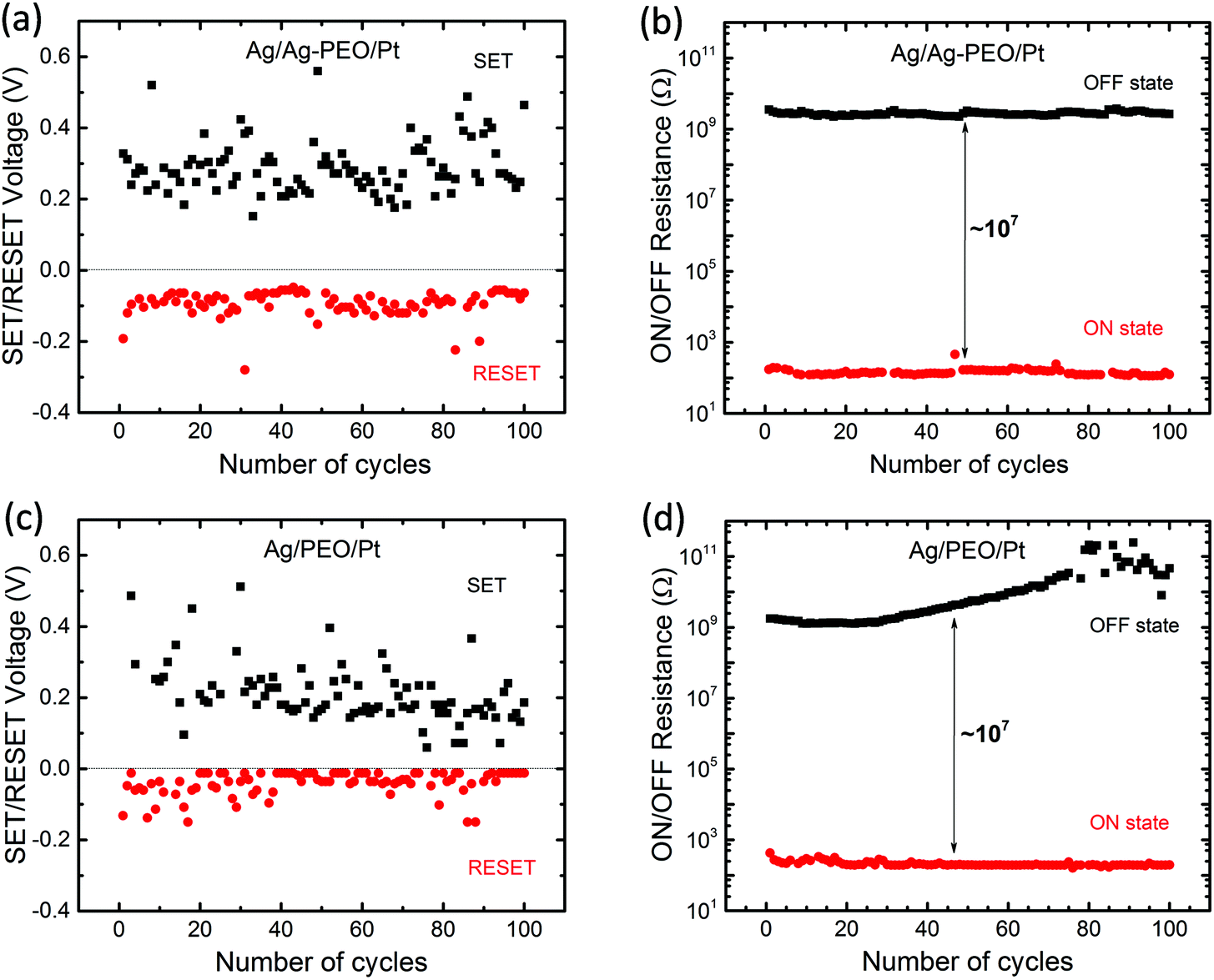 | ||
| Fig. 2 Endurance performance of ON/OFF resistances and SET/RESET voltages plotted as a function of the number of cycles for Ag/Ag–PEO/Pt (a & b), Ag/PEO/Pt (c & d) planar devices. | ||
Fig. 3a and c are SEM images of the Ag/Ag–PEO/Pt and Ag/PEO/Pt planar devices, respectively, taken after the 102 consecutive sweep cycles shown in Fig. 1c and d. The different filament formation behaviours in the two devices are clearly seen. In the Ag/Ag–PEO/Pt device, the filament formation appears to consist of Ag clusters randomly distributed throughout the PEO matrix, with connections between the electrodes occurring at several places. This random filament formation is ascribed to a large amount of pre-dissolved Ag+ ions in the PEO matrix, in addition to Ag+ ions supplied from the Ag electrode. In contrast, in the Ag/PEO/Pt device the electrodes seem to be connected by an aggregation of Ag clusters, although a lot of smaller clusters are also observed in the PEO matrix. In this case, all the observed Ag clusters in the PEO matrix arise solely from the Ag electrode, suppressing random filament growth. Magnified views of Fig. 3a and c are depicted in Fig. 3b and d, respectively. It is expected that the repeated switching cycles and higher ICC (Joule heating) lead to piling up of large clusters. The dissolution of the Ag electrode edge is clearly seen as evidence of Ag oxidation reactions under positive bias in the Ag–PEO device, as indicated by the circle in Fig. 3b. In the PEO device, the dissolution of the electrode edge is significantly reduced (Fig. 3d), which is probably due to the high crystallinity and lower ionic conductivity of the pure PEO matrix. Note that the images of Fig. 3 were taken in the OFF state. Even if we observed the ON state, the images exhibited identical filament morphology. This means that precipitated structures are not re-incorporated into the PEO matrix completely and the switching takes place at a very narrow gap in the filament structures.
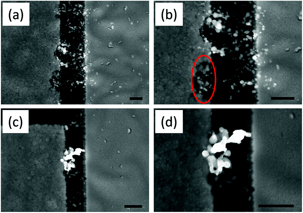 | ||
| Fig. 3 SEM image taken after 102 consecutive I–V sweeps for (a) Ag/Ag–PEO/Pt and (c) Ag/PEO/Pt planar devices with a gap distance of ∼1 and ∼0.5 μm, respectively. The left and right electrodes correspond to Ag and Pt, respectively. Images (b) and (d) are the corresponding magnified views. ICC was set at 1 mA and 400 μA for the Ag–PEO and PEO devices, respectively. The scale bar is 500 nm. | ||
According to the results obtained from I–V measurements and SEM observations, we speculate that filament growth dynamics depend strongly on the device configuration and the experimental conditions, which are most likely able to determine stable resistive switching characteristics. Hence, we performed a more detailed analysis of the filament growth dynamics so as to completely understand the conducting filament growth process–resistive switching property relationship.
Factors determining filament formation
We examined the filament growth behaviour after the forming process as a function of the gap distance, salt inclusion, and ICC. The forming process was terminated when the device was SET from the pristine state under positive bias sweeping with a sweep rate of 2 mV s−1 and a certain ICC. The bias voltage was limited to 10 V to avoid damage to the devices. The device was then transferred for SEM observations. At least five devices were examined for each case, and the representative images are shown here. We consider several kinetic factors that contribute to filament formation and discuss how these factors determine the growth processes.Gap distance
Fig. 4a–c are SEM images of Ag/Ag–PEO/Pt devices with different gap distances of ∼2, ∼1, and ∼0.5 μm after the forming process with ICC = 100 nA. Such a low compliance current was used to stop the initial stage of the filament growth processes. The corresponding I–V plots are depicted in Fig. 4d–f. All the SEM images exhibit dendritic filament morphologies, in which one of the filaments connects between the two electrodes. For the smallest gap distance (∼0.5 μm), narrower filaments grow randomly from the Pt electrode (Fig. 4c). As the gap distance increases, one of the filaments grows further and its morphology changes to a more dendritic formation, as seen in Fig. 4a and b. This indicates that the dendritic growth can be enhanced in devices with larger gap distances, although the filament growth is driven by the same dynamics. Low-power images also show the transition from a random formation of narrow filaments to dendritic dominated growth beyond a certain characteristic length (∼0.5 μm), as seen in Fig. S1 of the ESI.† Voids created in the Ag electrode evidence the oxidation of Ag (Ag → Ag+ + e−) under voltage bias and their area decreases when the gap distance is decreased, as indicated by the circles in Fig. 4b and c (also by the arrows in Fig. S1a–c†). This is because the number of Ag+ ions needed to form a filament between the electrodes is reduced for smaller gap distances. The forming voltage is also reduced from ∼0.49 to ∼0.33 V by decreasing the gap distance, as seen in Fig. 4d–f. This suggests that a smaller number of Ag+ ions are required for a filament to form for smaller gap distances. The filament seems to connect between the electrodes in all the devices in Fig. 4. However, if the bias voltage was swept back to the negative voltage direction subsequently, all the devices exhibited volatile switching behaviour. Because the ON resistance exceeds the resistance of a single atomic point contact (= 12.9 kΩ), the threshold switching, in which electron tunnelling through the precipitated structures is dominated, seems to be responsible for volatile behaviour at lower ICC.32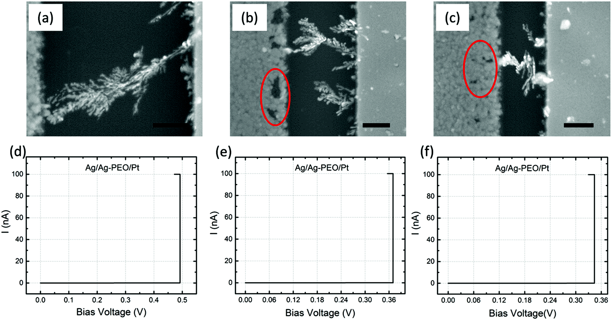 | ||
| Fig. 4 SEM images of the filament growth morphology between Ag (left side) and Pt (right side) electrodes, after the forming process, taken for Ag/Ag–PEO/Pt devices with gap distances of ∼2 (a), ∼1 (b), and ∼0.5 μm (c). The scale bar is 500 nm. Corresponding I–V plots, with a constant sweep rate of 2 mV s−1 and ICC of 100 nA, are shown in (d)–(f). | ||
The impact of the gap distance on the filament growth process is more pronounced for Ag/PEO/Pt devices, as shown in Fig. 5a–c; corresponding I–V plots are depicted in Fig. 5d–f. For the largest gap distance (∼2 μm), no completed filament formation occurred even after the bias voltage was applied up to ∼9.3 V (Fig. 5d), although some precipitations were observed on the Pt electrode, as indicated by the dashed arrows in Fig. 5a. This means that the PEO device cannot be SET for such a gap distance range under the bias condition used. However, if the gap distance was decreased to ∼1 μm, a very narrow filament, consisting of small Ag clusters, was observed to connect between the two electrodes (Fig. 5b), and a current jump to the compliance level was confirmed in the I–V plot (Fig. 5e), resulting in the forming process of the device. As the gap distance is decreased further, more than one filament formation appears between the electrodes (Fig. 5c shows two filaments), and the corresponding forming voltage is reduced from ∼4.2 to ∼2.8 V (see Fig. 5e and f). These results show that gap distance plays a critical role in the initial filament formation in the PEO device.
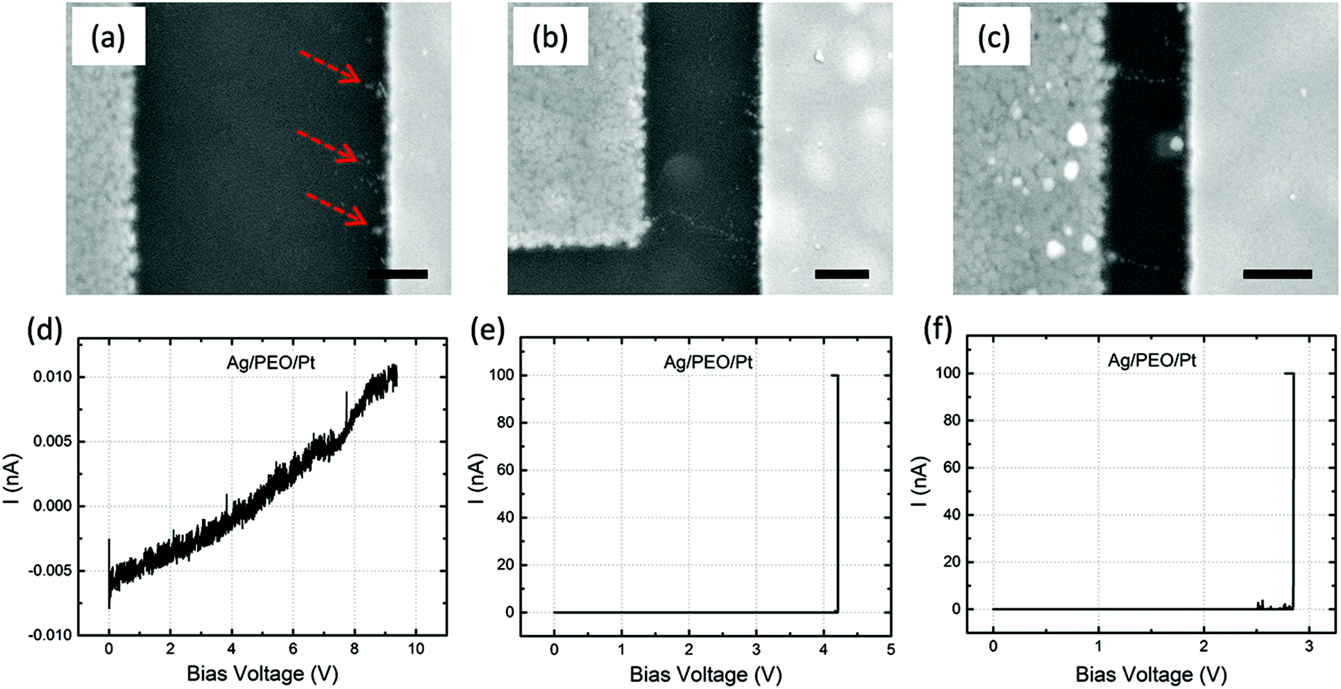 | ||
| Fig. 5 SEM images of the filament growth morphology between Ag (left side) and Pt (right side) electrodes, after the forming process, taken for Ag/PEO/Pt devices with gap distances of ∼2 (a), ∼1 (b), and ∼0.5 μm (c). The scale bar is 500 nm. Corresponding I–V plots, with a constant sweep rate of 2 mV s−1 and ICC of 100 nA, are shown in (d)–(f). | ||
To see the electric field effect, we measured the forming time under the application of constant bias voltages for different gap distances and evaluated the forming time as a function of electric field, as shown in Fig. S2 of the ESI.† It was found that the forming time decreases exponentially with the electric field, suggesting that the filament growth is facilitated by the electric field in both Ag–PEO and PEO devices and the cation transport seems to be the rate-limiting process. A similar electric field strength effect was observed for dielectric-based resistive memories.10
Salt inclusion
A comparison of the observations for Ag–PEO devices (Fig. 4) and PEO devices (Fig. 5) highlights the effect of the salt inclusion in the polymer matrix. In general, pure PEO is a highly crystalline polymer, most of which is in a crystalline phase with a small amount in an amorphous phase.33 Therefore, long-range Ag+ ion transport is significantly hindered, and its conductivity is lowered down to 10−9 S cm−1.23 The oxidation rate of Ag at the Ag/PEO interface should also be lowered. Under positive bias to the Ag electrode, Ag atoms are oxidized at the interface and the dissolved Ag+ ions transport into the PEO matrix toward the Pt electrode. The lower oxidation rate and lower conductivity require a higher bias voltage to promote the redox reaction at the interfaces and ionic transport in the PEO matrix. Nevertheless, no filament formation takes place and precipitations can only be induced on the Pt electrode for a gap distance of ∼2 μm under the bias conditions used, as seen in Fig. 5a. However, when the gap distance was decreased, filament formation between the electrodes became possible. The precipitated Ag atoms are considered to grow along the Ag+ ion transport pathways, resulting in a unidirectional filament growth, as seen in Fig. 5b and c. The observed filaments consist of small Ag clusters rather than being connected continuously. The electron tunnelling through the precipitated clusters is responsible for the forming process with lower ICC, as discussed above.When Ag salt is added into the pure PEO matrix, the situation changes drastically.34 The inclusion of 3 wt% salt lowers the crystallinity of the PEO matrix with dispersed Ag+ ions, resulting in the ionic conductivity being increased by more than two orders of magnitude.23 Under positive bias, Ag atoms are oxidized faster at the Ag/Ag–PEO interface relative to the Ag/PEO interface, because of the increased amount of an amorphous phase. The higher oxidation rate at the Ag/Ag–PEO interface is evidenced by a large number of voids in the Ag electrode, as shown in the low-power SEM images of Fig. S1.†
Both the Ag+ ions dissolved from the Ag electrode and the pre-dissolved Ag+ ions in the PEO matrix can migrate toward the Pt electrode under voltage bias. Once precipitations take place on the Pt electrode, precipitated Ag atoms grow further by incorporating Ag+ ions that are distributed in the PEO matrix. These Ag+ ions act as reduction sites where Ag+ ions capture free electrons injected from the Pt electrode and are reduced to Ag atoms (Ag+ + e− → Ag). As a result, the precipitated atoms form dendritic morphologies with tree-like branching structures, as seen in Fig. 4a–c. These results indicate the importance of salt inclusion in the polymer matrix in determining the filament growth behaviour.
The salt inclusion also affects the initial stability of the filament structure. In PEO devices, the filament formed at the forming process is easily dissolved, because of a lower ion concentration in the surrounding medium (large difference in the electrochemical potential). This causes the initial instability of the filament, observed as the current spikes in Fig. 1b. After several switching cycles, the filament is stabilized due to the increase of the Ag+ ion concentration around the filament. In contrast, Ag–PEO devices possess enough concentration of pre-dissolved Ag+ ions and these ions can support stable filament formation.
Compliance current
I–V plots show that ICC affects switching behaviour. To investigate the impact of ICC on filament growth behaviour, forming processes with different ICC were performed and subsequent SEM analyses were conducted. Fig. 6a and c show SEM images of Ag/Ag–PEO/Pt and Ag/PEO/Pt devices with a gap distance of ∼0.5 μm, respectively, taken after a forming process with an ICC of 10 μA. The corresponding I–V plots are depicted in Fig. 6b and d. The images are compared with Fig. 4c and 5c, which were measured with an ICC of 100 nA. For the Ag–PEO device, dendritic growth was enhanced with increasing ICC, with many tree-like branches forming between the electrodes. On the other hand, even with higher ICC the PEO device still exhibited narrow and unidirectional filaments, which consisted of larger Ag clusters than is the case with smaller ICC (see Fig. 5c and 6c). The number of filaments drastically increased and these filaments changed to inverted cone-like shapes with their bases at the Pt electrode, as indicated by the arrow in Fig. 6c. From these observations, it was confirmed that the density of filament structures is directly proportional to the applied ICC. The impact of larger ICC can also be seen in the low-power images in Fig. S3 of the ESI,† which are compared to Fig. S1c and S1f.† Note that the switching behaviour is still volatile with an ICC of 10 μA for both devices. Indeed, the PEO device exhibited a current fluctuation after the forming process, as seen in Fig. 6d. The threshold switching is presumably responsible for the volatile behaviour even at this ICC level.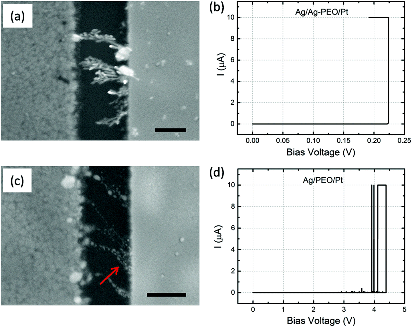 | ||
| Fig. 6 SEM images of (a) Ag/Ag–PEO/Pt and (c) Ag/PEO/Pt devices, taken after the forming process, with a constant sweep rate of 2 mV s−1 and ICC of 10 μA. The left and right electrodes correspond to Ag and Pt, respectively. The scale bar is 500 nm. Corresponding I–V plots are shown in (b) and (d) respectively. The gap distance was fixed to ∼0.5 μm for both devices. | ||
Comparison with the standard ECM model and other material systems
In general, the observed filament growth processes are comparable with the standard ECM model.13,14 In devices with inorganic solid electrolytes, like chalcogenides, the growth process is accompanied by a large volume of metal ions moving through the electrolyte and being reduced at the inert cathode, resulting in an inverted cone-shaped filament growing toward the active electrode.1,2 Devices based on dielectrics, such as SiO2, also exhibited filament growth processes initiating from the inert electrode. However, in some oxide materials like Al2O3, filament growth can be limited by the metal ion transport process, giving rise to a reduction of metal ions inside the dielectrics without their reaching the inert cathode, resulting in conducting filaments growing from the active electrode.10 A similar growth process was observed by a three-dimensional tomography technique based on conductive atomic force microscopy.9 Recently, two-dimensional kinetic Monte Carlo simulations reproduced both growth directions by taking into account various processes, such as fundamental redox reactions at the electrode–electrolyte interface and cation/electron hopping in the electrolyte.35,36 In our observations, filament growth always initiates from the Pt electrode, even for devices with pure PEO matrixes that have a lowered ionic conductivity. This means that the ECM model is applicable for the filament formation scheme in PEO-based atomic switches.Few studies have been reported on the observation of filament growth in organic material based devices, in comparison with devices using inorganic materials. Cho et al. investigated Ag filamentary paths in a polyfluorene derivative polymer film using a cross-sectional TEM technique.17 They observed the formation and rupture of Ag metallic bridges connecting Ag and heavily-doped Si electrodes after SET and RESET operations, respectively. However, filament growth between the electrodes has not been discussed in detail. Recently, Gao et al. observed the Ag filament growth process in planar devices using poly(3,4-ethylene-dioxythiophene):poly(styrenesulfonate) (denoted as PEDOT:PSS), which is used as a hole transport layer in organic field effect transistors.18 They found that cluster structures nucleate from the middle region in the gap between Ag and Pt electrodes and extend toward both electrodes. This anomalous behaviour was attributed to faster diffusion channels for Ag+ ions on the surface than in the interior of PEDOT:PSS films. In the present work, the transport of Ag+ ions is considered to take place in the interior of the PEO films, which results in filament growth processes appropriate for the standard ECM model with solid electrolytes and enables the precise examination of their parameter dependence.
To summarize the above findings, the filament formation processes in PEO-based atomic switches were found to be determined by the gap distance between the electrodes, the salt inclusion in the polymer matrix, and the compliance current applied in the measurements. These parameters are linked to kinetic factors such as the redox reaction rate at the interfaces, ion mobility in the matrix, electric field strength, and the reduction sites for precipitations. The results indicate that filament formation behaviour and the corresponding switching characteristics can be controlled by tuning the device configuration and experimental parameters.
Conclusions
The resistive switching characteristics and the corresponding conducting filament growth behaviours in PEO-based atomic switches have been systematically studied in a planar device configuration under the same experimental conditions. By decreasing the gap distance between the opposed Ag and Pt electrodes, the devices exhibited stable nonvolatile switching behaviour over 102 cycles, with high ON/OFF resistance ratios of ∼107. SEM observations after the forming process revealed that filament growth behaviour depends strongly on the device configuration and experimental parameters such as the gap distance, the salt inclusion in the PEO matrix, and the applied compliance current. These parameters are linked to kinetic factors determining the filament growth processes. First, salt inclusion has the most significant impact on the redox reaction rate at the anode interface, ion mobility in the PEO matrix, and the reduction sites for precipitations. These factors determine the filament formation morphology of unidirectional and dendritic growth processes and the magnitude of the forming voltages. Second, the gap distance determines the electric field strength affecting the filament morphology and provides the critical limit length for stable switching behaviour. Finally, the density and size of the grown filaments are controlled by the compliance current level and determine whether the switching behaviours are volatile or nonvolatile. It was also found that the observed filament growth processes are always consistent with the prediction of the standard ECM model for solid electrolytes, in which filament growth initiates from an inert electrode. These results contribute toward the complete understanding and control of not only resistive switching characteristics but also other unique properties, such as quantized conductance and the learning abilities of atomic switches using SPE.37,38Acknowledgements
The authors would like to thank A. Ohi and T. Ohki of MANA Foundry at NIMS for their assistance in the fabrication of the planar devices. This work was supported in part by JSPS KAKENHI Grant No. 24350278.Notes and references
- R. Waser and M. Aono, Nat. Mater., 2007, 6, 833–840 CrossRef CAS PubMed.
- R. Waser, R. Dittman, G. Staikov and K. Szot, Adv. Mater., 2009, 21, 2632–2663 CrossRef CAS.
- W. P. Lin, S. J. Liu, T. Gong, Q. Zhao and W. Huang, Adv. Mater., 2014, 26, 570–606 CrossRef CAS PubMed.
- Y. Yang and W. Lu, Nanoscale, 2013, 5, 10076–10092 RSC.
- B. K. You, W. I. Park, J. M. Kim, K. I. Park, H. K. Seo, J. Y. Lee, Y. S. Jung and K. J. Lee, ACS Nano, 2014, 8, 9492–9502 CrossRef CAS PubMed.
- K. Terabe, T. Hasegawa, T. Nakayama and M. Aono, Nature, 2005, 433, 47–50 CrossRef CAS PubMed.
- T. Ohno, T. Hasegawa, T. Tsuruoka, K. Terabe, J. K. Gimzewski and M. Aono, Nat. Mater., 2011, 10, 591–595 CrossRef CAS PubMed.
- T. Hasegawa, K. Terabe, T. Tsuruoka and M. Aono, Adv. Mater., 2012, 24, 252–267 CrossRef CAS PubMed.
- U. Celano, L. Goux, A. Belmonte, K. Opsomer, A. Franquet, A. Schulze, C. Detavernier, O. Richard, H. Bender, M. Jurczak and W. Vandervorst, Nano Lett., 2014, 14, 2401–2406 CrossRef CAS PubMed.
- Y. Yang, P. Gao, S. Gaba, T. Chang, X. Pan and W. Lu, Nat. Commun., 2012, 3, 732 CrossRef PubMed.
- Q. Lui, J. Sun, H. Lv, S. Long, K. Yin, N. Wan, Y. Li, L. Sun and M. Liu, Adv. Mater., 2012, 24, 1844–1849 CrossRef.
- X. Tian, L. Wang, J. Wei, S. Ynag, W. Wang, Z. Xu and X. Bai, Nano Res., 2014, 7, 1065–1072 CrossRef CAS.
- I. Valov, R. Waser, J. R. Jameson and M. N. Kozicki, Nanotechnology, 2011, 22, 254003 CrossRef PubMed.
- I. Valov and G. Staikov, J. Solid State Electrochem., 2013, 17, 365–371 CrossRef CAS.
- Y. Tang, P. Gao, L. Li, X. Pan, S. Tappertzhofen, S. H. Choi, R. Waser, I. Valov and W. D. Lu, Nat. Commun., 2014, 5, 4232 Search PubMed.
- X. Tian, S. Yang, M. Zeng, L. Wang, J. Wei, Z. Xu, W. Wang and X. Bai, Adv. Mater., 2014, 26, 3649–3654 CrossRef CAS PubMed.
- B. Cho, J. M. Yun, S. Song, Y. Ji, D. Y. Kim and T. Lee, Adv. Funct. Mater., 2011, 21, 3976–3981 CrossRef CAS.
- S. Gao, C. Song, C. Chen, F. Zeng and F. Pan, Appl. Phys. Lett., 2013, 102, 141606 CrossRef.
- S. Wu, T. Tsuruoka, K. Terabe, T. Hasegawa, J. P. Hill, K. Ariga and M. Aono, Adv. Funct. Mater., 2011, 21, 93–99 CrossRef CAS.
- S. R. Mohapatra, T. Tsuruoka, T. Hasegawa, K. Terabe and M. Aono, AIP Adv., 2012, 2, 022144 CrossRef.
- S. R. Mohaptra, T. Tsuruoka, K. Krishnan, T. Hasegawa and M. Aono, J. Mater. Chem. C, 2015, 3, 5715–5720 RSC.
- Y. Ji, B. Cho, S. Song, T. W. Kim, M. Choe, Y. H. Kahng and T. Lee, Adv. Mater., 2010, 22, 3071–3075 CrossRef CAS PubMed.
- U. S. Bhansali, M. A. Khan, D. Cha, M. N. Almadhoun, R. Li, L. Chen, A. Amassian, I. N. Odeh and H. N. Alshareef, ACS Nano, 2013, 7, 10518–10524 CrossRef CAS PubMed.
- J. J. Kim, B. Cho, K. S. Kim, T. Lee and G. Y. Jung, Adv. Mater., 2011, 23, 2104–2107 CrossRef CAS PubMed.
- Y. Ji, D. F. Zeigler, D. S. Lee, H. Choi, A. K.-Y. Jen, H. C. Ko and T.-W. Kim, Nat. Commun., 2013, 4, 2707 Search PubMed.
- F. Croce, G. B. Appetecchi, L. Persi and B. Scrosati, Nature, 1998, 394, 456–458 CrossRef CAS.
- A. M. Christie, S. J. Lilley, E. Staunton, Y. G. Andreev and P. G. Bruce, Nature, 2005, 433, 50–53 CrossRef CAS PubMed.
- K. Krishnan, T. Tsuruoka and M. Aono, Jpn. J. Appl. Phys., 2016, 55 CrossRef , 06GK02.
- K. Krishnan, T. Tsuruoka, C. Mannequin and M. Aono, Adv. Mater., 2016, 28, 640–648 CrossRef CAS PubMed.
- I. Valov, E. Linn, S. Tappertxhofen, S. Schmelzer, J. van den Hurk, F. Lentz and R. Waser, Nat. Commun., 2013, 4, 1771 CrossRef CAS PubMed.
- S. Tappertzhofen, I. Valov, T. Tsuruoka, T. Hasegawa, R. Waser and M. Aono, ACS Nano, 2013, 7, 6396–6402 CrossRef CAS PubMed.
- H. Sun, Q. Liu, C. Li, S. Long, H. Lv, C. Bi, Z. Huo, L. Li and M. Liu, Adv. Funct. Mater., 2014, 24, 5679–5686 CrossRef CAS.
- M. A. Ratner and D. F. Shriver, Chem. Rev., 1988, 88, 109–124 CrossRef CAS.
- T. M. A. Abrantes, L. J. Alcacer and C. A. C. Sequeira, Solid State Ionics, 1986, 18, 315–320 CrossRef.
- S. Qin, Z. Liu, G. Zhang, Y. Sun, H. Wu, H. Qian and Z. Yu, Phys. Chem. Chem. Phys., 2015, 17, 8627–8632 RSC.
- S. Menzel, P. Kaupmann and R. Waser, Nanoscale, 2015, 7, 12673–12681 RSC.
- S. Tappertzhofen, I. Valov and R. Waser, Nanotechnology, 2012, 23, 145703 CrossRef CAS PubMed.
- T. Tsuruoka, T. Hasegawa, K. Terabe and M. Aono, Nanotechnology, 2012, 23, 435705 CrossRef PubMed.
Footnote |
| † Electronic supplementary information (ESI) available. See DOI: 10.1039/c6nr00569a |
| This journal is © The Royal Society of Chemistry 2016 |