
 Open Access Article
 This Open Access Article is licensed under a
 Creative Commons Attribution 3.0 Unported Licence
Charge transfer and surface defect healing within ZnO nanoparticle decorated graphene hybrid materials†
Chuyen V.
Pham
ab,
Sergej
Repp
c,
Ralf
Thomann
b,
Michael
Krueger
*d,
Stefan
Weber
ce and
Emre
Erdem
*c
aLaboratory for MEMS Applications, Department of Microsystems Engineering - IMTEK, University of Freiburg, Georges-Koehler-Allee 103, 79110 Freiburg, Germany
bFreiburg Materials Research Center (FMF), University of Freiburg, Stefan-Meier-Str. 21, 79104 Freiburg, Germany
cInstitute of Physical Chemistry, University of Freiburg, Albertstr. 21, 79104 Freiburg, Germany. E-mail: emre.erdem@physchem.uni-freiburg.de
dCarl-von-Ossietzky University Oldenburg, Institute of Physics, Carl-von-Ossietzky Str. 9-11, D-26129 Oldenburg, Germany. E-mail: michael.krueger@uni-oldenburg.de
eFreiburg Institute for Advanced Studies (FRIAS), University of Freiburg, Albertstr. 19, 79104 Freiburg, Germany
First published on 11th April 2016
Abstract
To harness the unique properties of graphene and ZnO nanoparticles (NPs) for novel applications, the development of graphene–ZnO nanoparticle hybrid materials has attracted great attention and is the subject of ongoing research. For this contribution, graphene-oxide–ZnO (GO–ZnO) and thiol-functionalized reduced graphene oxide–ZnO (TrGO–ZnO) nanohybrid materials were prepared by novel self-assembly processes. Based on electron paramagnetic resonance (EPR) and photoluminescence (PL) investigations on bare ZnO NPs, GO–ZnO and TrGO–ZnO hybrid materials, we found that several physical phenomena were occurring when ZnO NPs were hybridized with GO and TrGO. The electrons trapped in Zn vacancy defects (VZn−) within the core of ZnO NPs vanished by transfer to GO and TrGO in the hybrid materials, thus leading to the disappearance of the core signals in the EPR spectra of ZnO NPs. The thiol groups of TrGO and sulfur can effectively “heal” the oxygen vacancy (VO+) related surface defects of ZnO NPs while oxygen-containing functionalities have low healing ability at a synthesis temperature of 100 °C. Photoexcited electron transfer from the conduction band of ZnO NPs to graphene leads to photoluminescence (PL) quenching of near band gap emission (NBE) of both GO–ZnO and TrGO–ZnO. Simultaneously, electron transfer from graphene to defect states of ZnO NPs is the origin of enhanced green defect emission from GO–ZnO. This observation is consistent with the energy level diagram model of hybrid materials.
ZnO nanomaterials have attracted great attention due to their unique magnetic, electronic, optical, and electromechanical properties.1,2 Moreover, their large exciton binding energy (60 meV) allows efficient excitonic lasing at room temperature.3 Therefore, ZnO nanomaterials have great potential for various applications such as spintronic devices, light-emitting diodes,4 solar cells,5 laser diodes, UV detectors,6,7 and field effect transistors.8 Meanwhile, it has been demonstrated that graphene is a highly promising material for various applications due to its outstanding optical, electrical and mechanical properties.9 For example, its extreme strength and flexibility makes bendable devices feasible.10 Electrical conductivity in combination with optical transparency makes graphene suitable for applications in optoelectronics,11 while its super-large specific area is beneficial for sensor applications or as a catalyst support.12,13 Recently, ZnO nanomaterials have been combined with graphene, thus forming hybrid materials to harness the unique properties of the two components and generate synergic abilities for novel applications.6,14–18 The hybrids possess fascinating properties, which are not only those two components, but are also novel ones arising from the electronic coupling between graphene and ZnO. For example, ZnO quantum dots (QD) were wrapped with graphene oxide (GO) to generate an additional energy band structure for excitons to occupy, thus leading to additional blue-light emissions. Afterwards, the hybrid material was used to fabricate a white-light emitting diode.19 In that work, however, the surface defect emission of ZnO QDs was not addressed. In later reports,12,20 ZnO/unoxidized graphene and ZnO/GO composite films were synthesized by ultrasonic-assisted spray pyrolysis. Their photoluminescence (PL) investigation showed strong and broad green emissions from the composite films while these were not observed in the ZnO film. Such emission behavior was indirectly explained with the reduced crystallinity of ZnO composite films through increasing oxygen vacancies in the presence of graphene. More recently, Kavitha et al.21 indicated that oxygen vacancy defect states were healed by diffusion of surface oxygen from GO to ZnO when GO was reduced during the pyrolytic synthesis of hybrid materials. The PL of rGO–ZnO hybrid materials was significantly quenched due to the charge transfer between ZnO and graphene sheets. Very recently, not only were enhanced photocurrent and photocatalytic22,23 responses reported for rGO–ZnO nanohybrids but antiferromagnetic behavior was also detected for cobalt doped hybrids.24
In the present work, graphene oxide (GO) and thiol-functionalized graphene (TrGO) were hybridized with ZnO NPs to form GO–ZnO and TrGO–ZnO hybrid materials. The healing effect of oxygen-functionalities within GO and thiol groups of TrGO on both the (VO+) surface defects was investigated and compared using EPR spectroscopy. Here, not only was the charge transfer between ZnO NPs and either GO or TrGO during hybrid formation and under illumination examined, but the influence of the charge transfer on PL emission spectra was also studied.
GO was synthesized using a modified Hummer's method as outlined in our previous report.15 The oxygen-containing groups, such as hydroxyl (OH) and carboxylic (COOH), serve as anchor points for ZnO NP attachment forming ZnO NP decorated GO hybrid materials (GO–ZnO). The GO was thiol-functionalized into TrGO by refluxing GO with phosphorus pentasulfide (P4S10) in dimethylformamide (DMF) at 154 °C for 24 h as reported elsewhere.25 The thiol groups were shown to exhibit strong affinity to semiconductor nanoparticles.25,26 In this work, we also report their high attraction towards ZnO NPs forming ZnO NP decorated TrGO (TrGO–ZnO) by a self-assembly process. Details of ZnO NPs, GO–ZnO, and TrGO–ZnO hybrid material syntheses can be found in the ESI.† The preparation and detailed characterisation of both GO25 and ZnO27 materials have been published elsewhere. Recently, it has been reported that graphene-based ZnO heterostructures give rise to an inhomogeneous strain distribution that is likely due to the mismatch of their thermal expansion coefficients.28
Fig. 1 shows TEM images of TrGO–ZnO (a) and GO–ZnO (b) hybrid materials. ZnO NPs were observed to attach to the graphene surface, and there are no ZnO NPs located outside the graphene sheets. This indicates that the hybrid materials were successfully synthesized via self-attachment.
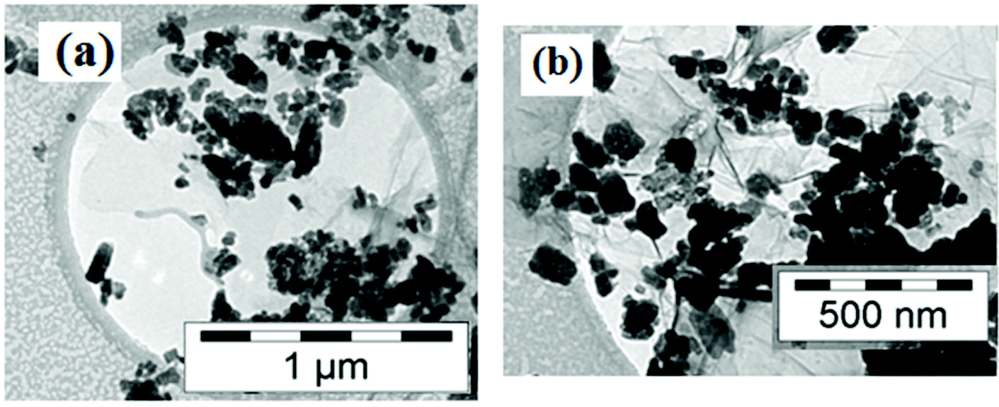 | ||
| Fig. 1 TEM images of a ZnO NP decorated GO sheet (a) and ZnO NP decorated TrGO sheet (b). | ||
For the case of CdSe–TrGO hybrid materials, it was demonstrated in a previous study29 that the formation of the hybrid completely changes the physical properties of individual components due to electronic coupling. ZnO NP surface defects have been detected using EPR and they are the cause of surface defect related PL emission in addition to bandgap transition PL emission.27,30,31 The anchors of ZnO NPs to rGO and TrGO are expected to result in the changes in EPR and PL emission spectra of individuals.
Fig. 2a (upper curve) reveals that the EPR spectrum of ZnO NPs comprises two signals: one with a g-factor at g1 = 2.0037 close to the value of the free electron (ge = 2.0023), and the other at g2 = 1.9600. The signal at g1 results from singly charged oxygen vacancies with unpaired electrons (VO+), and the signal centered at g2 is attributed to the core defects (VZn−) of the ZnO NPs.31,32 When ZnO NPs were attached to GO via oxygen-containing groups, the core signal disappears, as shown in Fig. 2a (lower curve). The signal at g3 = 2.0024 is due to the complex of a surface defect signal (at g1 = 2.0037) from ZnO NPs and a signal (at g = 2.0023) from carbon dangling bonds within GO, which is consistent with previous reports.19,29
 | ||
| Fig. 2 EPR signals of ZnO NPs and GO–ZnO hybrid materials (a), and rGO, TrGO, and TrGO (b). rGO exhibits low EPR signal intensity. Thiol-functionalization of GO to yield TrGO results in a high EPR intensity, and defect healing and charge transfer totally quench the EPR signals of both ZnO NPs and TrGO. EPR spectra of GO can be found elsewhere.25 | ||
The origin of intrinsic defects and their assignment both at the core and surface of ZnO nanocrystals are still controversial issues. Conceivably, probable intrinsic defect centers in ZnO are: (i) zinc vacancies, (ii) zinc on interstitial sites, (iii) oxygen on interstitial sites, and (iv) oxygen vacancies. EPR active intrinsic defect centers have been discussed in detail previously elsewhere.30,33 The disappearance of the core signals can be attributed to the charge transfer occurring between ZnO NPs and either GO or TrGO. This can be rationalized by using the well-established core–shell model for ZnO nanocrystals.31,34 According to this model, the core is negatively charged due to electrons being trapped in Zn vacancy defects (VZn−), while the shell contains singly charged oxygen vacancies as surface defects (Fig. 3). The electrons trapped in surface defects are well confined due to the dielectric nature of the surface of ZnO NPs. Therefore, these electrons are not transferred to electronic states of GO, but remain at the surface inducing the EPR signal at g3 = 2.0024 (Fig. 2a lower line). The electrons trapped in the core may be delocalized owing to the electrical mobility of the core.33–35 This leads to an interesting phenomenon occurring in the GO–ZnO and TrGO–ZnO hybrid materials: the electrons in the core delocalize to the surface, and are then transferred to GO and TrGO, as is schematically illustrated in Fig. 3.
 | ||
| Fig. 3 Schematic illustration of electron spin delocalization within GO–ZnO and TrGO–ZnO hybrid materials leading to the quenching of the core EPR signals. | ||
This happens because the energy-level matching between the conduction band (CB) of ZnO NPs and Fermi levels of GO and TrGO facilitates charge transfer. As shown in Fig. 4, the CB of ZnO NPs is about −4.19 eV slightly above the Fermi level of GO and TrGO,36 which are in a range from −4.5 to −4.7 eV.24 As a result, the electrons vanish in the core, thus leading to the disappearance of the core signals in both GO–ZnO and TrGO–ZnO hybrid materials.
 | ||
| Fig. 4 Schematic energy level diagram and charge transfer leading to PL quenching and enhanced defect emission in the GO–ZnO (left image) and TrGO (right image) hybrid materials. | ||
Fig. 2b displays EPR signals of rGO, TrGO, and TrGO–ZnO. While rGO exhibits very low EPR signal intensity, the sulfur-doping of TrGO introduces thiol groups into rGO generated dangling bonds within the lattice of graphene, thus resulting in a pronounced EPR signal at g4 = 2.0023. After hybridizing TrGO with ZnO NPs through thiol groups, both the EPR signals of TrGO and ZnO are completely quenched (Fig. 2b lowest line). This is remarkably different from the EPR behavior of GO–ZnO. Here, the quenching of the ZnO NP's core signal can be explained as in the case of GO–ZnO. The quenching of the surface defect signal can be attributed to the healing effects of thiol groups to oxygen vacancies in the surface defects. Moreover, during synthesis, traces of a free sulfur byproduct may remain in TrGO.15 The sulfur will also fill the oxygen vacancies of ZnO NPs at the surface areas, which are not wrapped by TrGO, as shown in Fig. 3. Thus, it can be concluded that the oxygen vacancy defects were completely healed in TrGO–ZnO hybrid materials. Such effects can also be confirmed by investigations using PL spectroscopy, which will be described below. However, before going to that, here one interesting question arises: why is the EPR signal of TrGO quenched, but that of GO persists when hybridized with ZnO NPs? A reasonable answer for this question is as follows: after the electrons were transferred from ZnO to TrGO, they hopped within the TrGO lattice because TrGO has high charge mobility as was proven by our previous work.25 The transferred electron spins couple with localized electron spins in TrGO, and as a consequence, the EPR signal of TrGO is quenched. In contrast, GO is dielectric so that the transferred electrons cannot hop to couple with the localized electron spins within the GO lattice, and therefore, the EPR signal of GO persists (Fig. 3).
To further corroborate the above hypotheses drawn from our EPR results, PL investigations were additionally performed. As schematically illustrated in Fig. 4, the free electrons in the CB (−4.19 eV) of ZnO NPs are favorably transferred to GO and TrGO (Fermi level: −4.5 to −4.7 eV)37,38 so that the PL intensity of the bandgap emission is expected to decrease. In the reverse direction, electrons can also be transferred from graphene to defect states (defect level: −5.25 eV) of ZnO NPs, thus increasing the amount of electrons in defect states. This is expected to lead to the enhancement of the defect emission PL band of GO–ZnO. By contrast, in the TrGO–ZnO hybrid, the surface defects of ZnO NPs are healed, so that their defect emission is expected to be quenched.
In fact, the PL spectra of ZnO NPs, GO–ZnO, and TrGO–ZnO (Fig. 5) behave exactly as predicted above. The PL spectrum of ZnO NPs exhibits two maxima: one sharp peak from bandgap emission at 377 nm which is related to near-band-edge emission (UV-emission) and one broad band from defect related emission centered at 525 nm (green emission). The intensities of bandgap emissions are drastically quenched in GO–ZnO and TrGO–ZnO samples as compared to free ZnO NPs, whereas the defect emission band of GO–ZnO is increased. This leads to a peak maximum ratio between defect emission (IDE) and bandgap emission (IBG), IBG/IDE, of 1.01 for bare ZnO NPs and 7.52 for ZnO NP decorated GO. For TrGO–ZnO, the defect emission band is drastically quenched due to the healing of surface defects as described and discussed above.
 | ||
| Fig. 5 Comparison of PL spectra showing the PL quenching of both bandgap and defect emission in TrGO–ZnO (black line), whereas only bandgap emission is quenched for GO–ZnO (red line). | ||
The results from PL investigations are consistent with those from EPR, and taken together, they strongly support the charge-transfer model drawn from the energy-level diagram (Fig. 4). It is noteworthy that the broad defect emission band of GO–ZnO exhibits a red-shift as compared to that of ZnO NPs. This could be due to the interaction of surface defect states and the π-electron cloud of the graphene lattice.21
Conclusions
GO–ZnO and TrGO–ZnO hybrid materials were synthesized by a novel self-assembly process. EPR and PL results demonstrate that electron spins trapped in Zn vacancy defects (VZn−) within the core of ZnO NPs move to the surface and are then transferred to GO and TrGO in the hybrid materials thus leading to the disappearance of core signals from EPR spectra for ZnO NPs. Thiol groups of TrGO and sulfur can effectively heal the oxygen vacancy surface defects of ZnO NPs while oxygen-containing functionalities have low healing ability at low temperature. The electrons transferred from ZnO NPs can hop in the TrGO lattice and their spins couple with localized electron spins thus leading to the quenching of the EPR signal of TrGO. In contrast, this does not occur in GO due to its low charge mobility. Charge transfer from graphene to the defect states of ZnO NPs is the origin of enhanced green defect emission of GO–ZnO. The hybridization of ZnO NPs and graphene results in synergistic properties of the individuals, or even creates new properties. For example, the enhancement of green emission of GO–ZnO has potential for visible light emitting diode application.2 The charge transfer occurring within the hybrids can be useful in photodetector applications.39 We believe that these findings contribute to a deeper understanding of physical and chemical processes occurring in graphene–ZnO hybrid materials and their use for applications.Competing interest
The authors declare no competing financial interest.Acknowledgements
We thank the “German Science Foundation” (DFG) (Er 662/1-2) and the “Vietnam International Education Development” (VIED) program for financial support.References
- K. Ando, Science, 2006, 312, 1883–1885 CrossRef CAS PubMed.
- D. I. Son, B. W. Kwon, D. H. Park, W.-S. Seo, Y. Yi, B. Angadi, C.-L. Lee and W. K. Choi, Nat. Nanotechnol., 2012, 7, 465–471 CrossRef CAS PubMed.
- U. Ozgur, Y. I. Alivov, C. Liu, A. Teke, M. A. Reshchikov, S. Dogan, V. Avrutin, S. J. Cho and H. Morkoc, J. Appl. Phys., 2005, 98, 041301 CrossRef.
- X. W. Sun, J. Z. Huang, J. X. Wang and Z. Xu, Nano Lett., 2008, 8, 1219–1223 CrossRef CAS PubMed.
- J. J. Cole, X. Wang, R. J. Knuesel and H. O. Jacobs, Nano Lett., 2008, 8, 1477–1481 CrossRef CAS PubMed.
- V. S. Dang, Y. Y. Song, N. Q. Hoa, S. C. Yu and Y. G. Yoo, J. Korean Phys. Soc., 2008, 52, 1398–1401 CrossRef CAS.
- Z. Wang, X. Zhan, Y. Wang, S. Muhammad, Y. Huang and J. He, Nanoscale, 2012, 4, 2678–2684 RSC.
- W. Song, S. Y. Kwon, S. Myung, M. W. Jung, S. J. Kim, B. K. Min, M.-A. Kang, S. H. Kim, J. Lim and K.-S. An, Sci. Rep., 2014, 4, 4064 Search PubMed.
- K. S. Novoselov, V. I. Fal'ko, L. Colombo, P. R. Gellert, M. G. Schwab and K. Kim, Nature, 2012, 490, 192–200 CrossRef CAS PubMed.
- S. Bae, H. Kim, Y. Lee, X. Xu, J.-S. Park, Y. Zheng, J. Balakrishnan, T. Lei, H. R. Kim, Y. I. Song, Y.-J. Kim, K. S. Kim, B. Ozyilmaz, J.-H. Ahn, B. H. Hong and S. Iijima, Nat. Nanotechnol., 2010, 5, 574–578 CrossRef CAS PubMed.
- H. Wang and Y. H. Hu, Energy Environ. Sci., 2012, 5, 8182–8188 CAS.
- N. G. Sahoo, Y. Pan, L. Li and S. H. Chan, Adv. Mater., 2012, 24, 4203–4210 CrossRef CAS PubMed.
- G. Wang, Z. Li, M. Li, J. Liao, C. Chen, S. Lv and C. Shi, Phys. Chem. Chem. Phys., 2015, 17, 31822–31829 RSC.
- O. Akhavan, ACS Nano, 2010, 4, 4174–4180 CrossRef CAS PubMed.
- H. Chang, Z. Sun, K. Y.-F. Ho, X. Tao, F. Yan, W.-M. Kwok and Z. Zheng, Nanoscale, 2011, 3, 258–264 RSC.
- B. Li and H. Cao, J. Mater. Chem., 2011, 21, 3346–3349 RSC.
- C. Song, K. W. Geng, F. Zeng, X. B. Wang, Y. X. Shen and F. Pan, Phys. Rev. B: Condens. Matter, 2006, 73, 024405 CrossRef.
- J. M. Lee, Y. B. Pyun, J. Yi, J. W. Choung and W. I. Park, J. Phys. Chem. C, 2009, 113, 19134–19138 CAS.
- S. S. Rao, A. Stesmans, Y. Wang and Y. Chen, Physica E, 2012, 44, 1036–1039 CrossRef CAS.
- E. Lee, J. Y. Kim, B. J. Kwon, E. S. Jang and S. J. An, Phys. Status Solidi RRL, 2014, 8, 836–840 CrossRef CAS.
- M. K. Kavitha, P. Gopinath and H. John, Phys. Chem. Chem. Phys., 2015, 17, 14647–14655 RSC.
- N. Song, H. Fan and H. Tian, Appl. Surf. Sci., 2015, 353, 580–587 CrossRef CAS.
- X. Wu, L. Wen, K. Lv, K. Deng, D. Tang, H. Ye, D. Du, S. Liu and M. Li, Appl. Surf. Sci., 2015, 358, 130–136 CrossRef CAS.
- Z. Xiang, J. Qian, Y. Zhou, F. Liu, C. Qi, X. Shi, G. Wang and S. Ye, Mater. Lett., 2015, 161, 286–288 CrossRef CAS.
- C. V. Pham, M. Eck and M. Krueger, Chem. Eng. J., 2013, 231, 146–154 CrossRef CAS.
- J. R. Mann and D. F. Watson, Langmuir, 2007, 23, 10924–10928 CrossRef CAS PubMed.
- S. Repp and E. Erdem, Spectrochim. Acta, Part A, 2015, 152, 637–644 CrossRef PubMed.
- G.-H. Nam, S.-H. Baek, C.-H. Cho and I.-K. Park, Nanoscale, 2014, 6, 11653–11658 RSC.
- C. V. Pham, M. Krueger, M. Eck, S. Weber and E. Erdem, Appl. Phys. Lett., 2014, 104, 132102 CrossRef.
- E. Erdem, J. Alloys Compd., 2014, 605, 34–44 CrossRef CAS.
- H. Kaftelen, K. Ocakoglu, S. Tu, R. Thomann, S. Weber and E. Erdem, Phys. Rev. B: Condens. Matter, 2012, 86, 014113 CrossRef.
- A. Prakash, S. K. Misra and D. Bahadur, Nanotechnology, 2013, 24 Search PubMed.
- S. K. S. Parashar, B. S. Murty, S. Repp, S. Weber and E. Erdem, J. Appl. Phys., 2012, 111, 113712 CrossRef.
- J. J. Schneider, R. C. Hoffmann, J. Engstler, A. Klyszcz, E. Erdem, P. Jakes, R. A. Eichel, L. Pitta-Bauermann and J. Bill, Chem. Mater., 2010, 22, 2203–2212 CrossRef CAS.
- P. Jakes and E. Erdem, Phys. Status Solidi RRL, 2011, 5, 56–58 CrossRef CAS.
- X. D. Zhou, X. H. Xiao, J. X. Xu, G. X. Cai, F. Ren and C. Z. Jiang, EPL, 2011, 93 CAS.
- P. V. Kumar, M. Bernardi and J. C. Grossman, ACS Nano, 2013, 7, 1638–1645 CrossRef CAS PubMed.
- N. Zhu, K. Zheng, K. J. Karki, M. Abdellah, Q. Zhu, S. Carlson, D. Haase, K. Zidek, J. Ulstrup, S. E. Canton, T. Pullerits and Q. Chi, Sci. Rep., 2015, 5 Search PubMed.
- D. Vinh Quang, T. Tran Quang, D.-I. Kim, D. Le Thai, B.-U. Hwang, D.-W. Lee, B.-Y. Kim, T. Le Duc and N.-E. Lee, Small, 2015, 11, 3054–3065 CrossRef PubMed.
Footnote |
| † Electronic supplementary information (ESI) available. See DOI: 10.1039/c6nr00393a |
| This journal is © The Royal Society of Chemistry 2016 |