
 Open Access Article
 This Open Access Article is licensed under a
 Creative Commons Attribution 3.0 Unported Licence
Understanding the interaction between energetic ions and freestanding graphene towards practical 2D perforation†
Jakob
Buchheim
a,
Roman M.
Wyss
a,
Ivan
Shorubalko
*b and
Hyung Gyu
Park
*a
aNanoscience for Energy Technology and Sustainability, Department of Mechanical and Process Engineering, Eidgenössische Technische Hochschule (ETH) Zürich, Tannenstrasse 3, CH-8092 Zürich, Switzerland. E-mail: parkh@ethz.ch
bLaboratory for Reliability Science and Technology, Empa (Swiss Federal Laboratories for Materials Science and Technology), Überlandstrasse 129, CH-8600 Dübendorf, Switzerland. E-mail: ivan.shorubalko@empa.ch
First published on 18th March 2016
Abstract
We report experimentally and theoretically the behavior of freestanding graphene subjected to bombardment of energetic ions, investigating the capability of large-scale patterning of freestanding graphene with nanometer sized features by focused ion beam technology. A precise control over the He+ and Ga+ irradiation offered by focused ion beam techniques enables investigating the interaction of the energetic particles and graphene suspended with no support and allows determining sputter yields of the 2D lattice. We found a strong dependency of the 2D sputter yield on the species and kinetic energy of the incident ion beams. Freestanding graphene shows material semi-transparency to He+ at high energies (10–30 keV) allowing the passage of >97% He+ particles without creating destructive lattice vacancy. Large Ga+ ions (5–30 keV), in contrast, collide far more often with the graphene lattice to impart a significantly higher sputter yield of ∼50%. Binary collision theory applied to monolayer and few-layer graphene can successfully elucidate this collision mechanism, in great agreement with experiments. Raman spectroscopy analysis corroborates the passage of a large fraction of He+ ions across graphene without much damaging the lattice whereas several colliding ions create single vacancy defects. Physical understanding of the interaction between energetic particles and suspended graphene can practically lead to reproducible and efficient pattern generation of unprecedentedly small features on 2D materials by design, manifested by our perforation of sub-5 nm pore arrays. This capability of nanometer-scale precision patterning of freestanding 2D lattices shows the practical applicability of focused ion beam technology to 2D material processing for device fabrication and integration.
Introduction
Discovery of isolated and stable graphene has launched a new research field to explore a variety of unforeseen properties of this two-dimensional (2D) material.1 In particular, graphene has drawn significant attention by showing extraordinary mechanical strength,2 great electrical3 and thermal conductivities,4 and virtually uninhibited transmission of light5 yet hermetic sealing against material permeation.6 Potential graphene-based technology is proposed for various applications including ultimately permeable membranes7 and flexible electronics,8 embodiment of which can be propelled by large-scale synthesis methods such as chemical vapour deposition (CVD).9,10 Device integration of graphene to exploit its unique properties, on the other hand, will require selective patterning via etching or crystallographic modification through exposure to plasma11 or energetic ions.12 The evolution of the electrical properties and quality of supported or sandwiched graphene subjected to ion irradiation has been investigated,13–18 all confirming that graphene can be patterned by energetic ion irradiation. Nevertheless, it is the presence of a support structure that obscures a mechanistic understanding of the effects of ion bombardment on a 2D lattice of graphene because the bulk sputtering mechanism of the support19 perplexes the otherwise clearly observable 2D sputtering mechanism. For example, the effects of the secondary cascade interaction of bombarding particles with the support layer, such as ion implantation and substrate swelling,13,15,20 can influence experimental results significantly, eventually hampering the extraction of the 2D sputtering mechanism and the construction of fine features on a nanometer scale. On the other hand, freestanding graphene has been patterned using transmission electron microscopy where pores21 and vacancies22 can be created with very high precision but are limited in scale due to immense irradiation dose required. Nanometer-sized feature formation in graphene has been enabled by block-copolymer self-assembly23 as well as by strain assisted metal intercalcination,24 both limited to feature sizes of ∼20 nm. In the pattern-size regime, other than these values, a focused ion beam (FIB) milling process of freestanding graphene can be a promising technology for practical applications at intermediate scales, considering that the FIB capability of nanoscale patterning under no such influence of substrates is adverse to fine feature-size control. Recently, the possibility of pattern generation in freestanding graphene by ion irradiation has been demonstrated by the formation of nanoscale pores,7,25 nanoribbons26 or other geometries,27 though these studies lack a mechanistic understanding of the energetic-ion–graphene interaction. More insight into the interaction has been obtained by a few theoretical investigations using Monte Carlo simulations.17,18,28 Despite the growing understanding of the 2D sputtering mechanism including graphene amorphization upon Ga+ irradiation,29 there are few reports of a combined experimental and theoretical investigation on the fate of freestanding graphene layers subjected to ion bombardment of various ion species and energies, hampering exploitation of the advanced manufacturing capability of the ion bombardment on freestanding graphene.Here, we investigate experimentally and theoretically the effect of ion bombardment on freestanding graphene. The use of clean micrometer-wide suspended graphene allows us to determine quantitatively the probability and rates of carbon atom removal by avoiding substrate-caused ion sputtering artifacts. We differentiate interaction schemes of energetic ions with the graphene layer. Depending on their size and kinetic energy, ions can either penetrate the freestanding graphene without sputtering or collide with atoms of the 2D crystal to produce various vacancies. We rationalize these interactions by binary collision processes between incident ions and carbon atoms of the graphene lattice. In good agreement with experimental results, our model further elucidates the ion interaction mechanism with freestanding graphene. According to the results, interatomic lattice spacing of graphene can render it semi-transparent to incident energetic ions and tolerant to sputtering. The present work closes the gap between verification of theoretical predictions and practical formation of array patterns on freestanding graphene. An understanding of the nature of the energetic ion beam interaction with 2D materials of graphene enables pattern perforation on graphene by design, leading to an unprecedented dimension of reproducible graphene pore patterning via FIB milling such as sub-4 nm and sub-3 nm hole-arrays using Ga+ and He+ FIB, respectively.
Experimental
Freestanding graphene sample preparation
Polycrystalline graphene was synthesized via CVD using conditions optimized for continued monolayer coverage reported elsewhere.30 A Cu foil (Alfa Aesar 46986) is cleaned by Ar ion beam milling (10 min at 250 mA, 600 V acceleration) prior to a reduction annealing in a H2-rich atmosphere (100 sccm H2 in 1500 sccm Ar) at 950 °C for 30 min. Growth is initiated by the addition of 25 sccm C2H4 to the chamber for 2 min and subsequently 50 sccm for 1 min. The as-grown monolayer graphene was transferred onto a punctured SiNx membrane supported by a Si chip (destination substrate) using a wet transfer method.7 PMMA is spun onto the graphene-coated Cu foil. Cu is etched away in (NH4)2S2O8 (0.5 M) leaving the graphene/PMMA film afloat the etchant. For multilayer graphene samples, this graphene/PMMA film is fished after rinsing in DI water with another graphene-grown Cu foil, and the additional Cu substrate is etched again. Repeating this step until the desired number of layers is reached, a clean multilayer graphene sample without interlayer contamination is obtained. After a final rinsing in DI water the floating graphene/PMMA film is fished with the porous SiNx destination substrate. Upon drying the graphene/PMMA film, the graphene is cleaned using well-known thermal decomposition methods31,32 where PMMA is pyrolyzed away at 400 °C in 900 sccm H2 and 100 sccm Ar, yielding clean freestanding graphene.Graphene characterization
The quality and cleanliness of the graphene samples were confirmed using scanning electron microscopy (Helios 450, FEI). Furthermore, the transferred graphene was analyzed before and after the patterning by 2D Raman mapping (micro Raman CRM200, WiTec) using a 532 nm incident laser beam at 0.4 mW with a pixel spacing of 100–250 nm.Ion irradiation
The freestanding graphene layers were irradiated with ions at different acceleration voltages via FIB (Helios 450, FEI). Toward the graphene sample Ga+ ions are accelerated at 5–30 keV with probe currents ranging from 1.1 pA to 40 pA and a chamber pressure of ∼7 × 10⁻⁵ Pa. For the He+ ion irradiation we used a He ion microscope (Zeiss Orion) equipped with a pattern generator (Raith Elphy MultiBeam) operated at 10–30 keV using a probe current of 5–17.5 pA at a chamber pressure of ∼7 × 10⁻⁵ Pa. Note that relatively high probe currents are desirable to reduce ion-beam-induced deposition in the exposed areas (ESI†). On both tools the ion dose was controlled by the exposure dwell time of each pixel ranging from 100 ns to 8 ms.Experimental sputter yield determination
The sputter yield (γ), defined as the average removal rate of carbon atoms from the graphene lattice, was determined by the following experiment. Circular pattern arrays of ions are accelerated toward freestanding graphene with increasing areal doses (σ). On each circular pattern the energetic ions are evenly distributed with 200 nm in diameter (nominal area An = 0.0314 μm2). After the patterning we acquire SEM micrographs and measure the resulting pattern area Ap using an image analysis program (ImageJ). The lower bound number of removed carbon atoms NC = σCApN can be easily calculated by using the areal density of carbon in graphene σC (m−2) and the number of graphene layers, N. The sputter yield is defined as γion = NC/Nion, where Nion = σionAn is the total number of ions irradiating the graphene layer.Graphene pore characterization
The sizes of pore arrays in double layer graphene were determined using high-resolution SEM images obtained on a FEI Helios 450 at 5 keV and 13 pA probe current collecting secondary electrons. The micrograph was analyzed (ImageJ) by identifying the circular pore area by the dark regions (no secondary electrons generated), from which the diameter or the pore dimension was calculated. Electron micrographs of the smallest pores created in monolayer graphene were obtained using a Hitachi SU8230 SEM at 30 keV and 55 pA probe current and equipped with an SEM detector for a bright-field transmission electron mode (aperture size: 1 mm). The pore area appears as a bright area where electrons pass the sample without being scattered. The micrographs were analyzed using the Gatan Digital Micrograph image analysis software.Results and discussion
Measurement of graphene sputter yield
A high degree of control of three synthesis steps of graphene device fabrication (CVD graphene growth, transfer, and a subsequent annealing process) yielded ultraclean, freestanding graphene samples (Fig. 1a) showing very few graphene wrinkles and sparse contamination sites. These samples transferred to the FIB chamber were irradiated with energetic ions. When exposed to He+ irradiation, graphene was resistant to a high dose of ions bombarding the monolayer. We could take images of freestanding monolayer graphene repeatedly at a standard imaging dose (σHe+ ≈ 1018 m−2) of the helium ion microscope (HIM) without significant damage to the samples, in agreement with previous findings.33,34 The power of HIM and the cleanliness of the graphene samples allow us to clearly distinguish the layer numbers of freestanding multilayer graphene (Fig. 1b).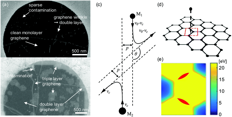 | ||
| Fig. 1 (a) SEM micrograph of freestanding clean monolayer CVD graphene after transfer to porous SiNx substrate. Brighter lines show graphene wrinkles (double layer) and small bright dots are sparse contaminates of graphene. (b) Helium ion micrograph of a He+ patterned freestanding double layer graphene membrane. Local number variations of graphene layers can be clearly distinguished by pronounced brightness changes. (c) Binary collision model illustrated in a center-of-mass reference frame moving at a speed of vc, where collision parameters p and θ are the shortest projected distance and the scattering angle between two colliding particles, respectively (following ref. 19). (d) Schematic of the ion bombardment process of freestanding monolayer graphene. A red dashed box illustrates a unit cell of graphene. (e) A contour of superimposed energy from 15 keV Ga+ to carbon atoms in a graphene unit cell, calculated from the binary collision model. The red shaded area depicts the area of double vacancy production. | ||
However, in the same experiment on a FIB system using Ga+ ions, we found that the freestanding graphene quickly deteriorated and was etched away. These findings indicate that the interaction between Ga+ and carbon in the graphene lattice is more destructive than that between He+ and graphene; namely, a Ga+ ion has a higher probability to chop off carbon atoms from the 2D lattice than a He+ ion. To precisely quantify the difference in carbon atom removal, the sputter yield is determined by patterning 200 nm circular features into monolayer graphene. The average number of vacancies produced per ion bombardment, or a sputter yield γ, shows a significantly higher value for Ga+ (Fig. 2a). For instance, the sputter yield of freestanding graphene upon 30 keV Ga+ bombardment is about 47% (γGa+ ≈ 47%), which confirms the qualitative findings of previous reports on Ga+-based graphene sputtering.27,35 This corresponds to a total ion dose necessary to create a pattern in monolayer graphene by 30 keV Ga+ ions of ∼8.1 × 10¹⁹ m−2 (Fig. 2b), which is very much in line with a recent report29 of 9.5 × 10¹⁹ m−2 for Ga+ at 35 keV. Furthermore, in our experiments γ of freestanding monolayer graphene showed clear dependency on the energy of the incident particles. For Ga+ the reduction of the accelerating voltage from 30 kV to 5 kV increases the sputter yield from γGa+ ≈ 47% to 81% (Fig. 2a), in line with predictions of Monte Carlo molecular dynamics simulations.17,18 Interestingly, these γGa+ values of monolayer graphene are significantly smaller than those of its 3D counterpart: reportedly 120–270% depending on carbon allotropes.35,36 For He+ FIB the sputtering yield is about two-orders-of-magnitude lower (γHe+ ≈ 0.7%) than that for Ga+ FIB. Therefore, pattern generation with 30 keV He+ ions requires a significantly higher dose of ∼5.7 × 10²¹ m−2 (Fig. 2b). Reaffirming the mechanism of HIM imaging,33,34 our finding sheds a renewed light on the possibility that, not only to protons,37,38 graphene can be nearly transparent to energetic He+ ions as shown theoretically.17 For example, at a kinetic energy of 30 keV approximately 99% of He+ ions can penetrate through the monolayer graphene with statistically sputtering few or no carbon atoms from the lattice, reminiscent of the photon and proton transmission. The material transparency of graphene is slightly reduced at lower He+ acceleration voltages (γHe+, 10 keV ≈ 2.4%, Fig. 2a) yet only to ∼97.6%. Both observations of the material transmission of H+ (ref. 37 and 38) and He+ through the defect-free graphene lattice offers a new insight into the ability of graphene to serve as the barrier material. In the case of increased particle energy or commensurable particle size, graphene crystals in their freestanding state (let alone crystallographic defects) indeed allow the permeation of small atoms through the lattice.
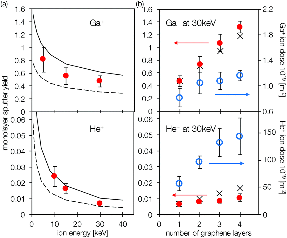 | ||
| Fig. 2 (a) Energy dependent monolayer graphene sputter yields. Lower and upper bounds of theoretical sputter yield for Ga+ and He+ using a binary collision model (dashed black line and solid black line, respectively). Red dots are measured sputter yield for Ga+ and He+ ions, with error bars indicating the standard deviation. Each data point is calculated as the mean of more than 20 independent measurements. (b) Layer number dependent sputter yield and ion dose necessary to pattern graphene using 30 keV Ga+ and He+ ions. Red dots show sputter yield for 1–4 freestanding layers of graphene, and error bars indicate the standard deviation. Black crosses indicate the expected sputter yield assuming the layer number independent probability of carbon atom removal upon collision. The blue circle shows the experimentally measured ion dose for pattern formation. | ||
Calculation of theoretical sputter yield
Since graphene is a 2D crystal of regularly bonded carbon atoms, its sputtering process can be assumed as a series of independent collision events between a bombarding ion and a lattice-bonded carbon atom individually. This interaction is then modeled by the use of the classic binary collision theory19,39 on the basis of an interception of two particle trajectories where the energetic ion at a velocity v0 collides with a carbon atom at a velocity vc (Fig. 1c). Depending on the minimum projected distance between two particle trajectories, p, the nuclei start repelling each other to avoid overlap of the coulombic potential of the nuclei. The scatter angle, θ, upon the interception (or collision) can be calculated using eqn (1): | (1) |
 is given by a repulsive coulombic potential created by the charges carried by the two nuclei corrected by a universal bfit function
 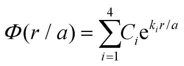 accounting for the electron cloud screening effects. The fit function depends on the distance of the scattering particles, r, the screening length, a = 0.8854a0(Z10.23 + Z20.23)−1, calculated by the use of the Bohr radius, a0, the two atomic charges Z1 and Z2 and has 8 parameters C1 = 0.1818, C2 = 0.5099, C3 = 0.2802, C4 = 0.02811 and k1 = −3.2, k2 = −0.9423, k3 = −0.4029, k4 = −0.2016.19 It is valid for collisions with kinetic energies higher than a few 100 eV, where interatomic interactions are governed primarily by repulsive nuclei such that the Born–Oppenheimer approximation can be omitted.40 For each scatter angle, one can calculate the energy transferred, T, from the ion to the atom:
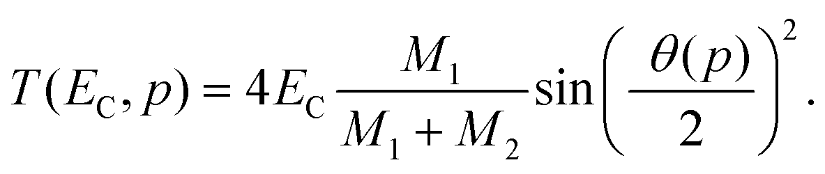 | (2) |
A carbon atom is removed from the graphene lattice if the transferred energy, T(EC,p), exceeds the lattice displacement energy, EL. Previously reported EL values for graphene range from experimentally determined 22 eV (ref. 41) to density-functional-theory predicted 23 eV.42,43 Assuming EL remains constant by neglecting vibrations of and locally altered binding energy of a defective graphene lattice in the course of sputter etching, we use this energy cut-off to calculate a theoretical sputter yield of graphene. Considering a graphene unit cell (Fig. 1d) with the superimposed transferred energy landscape around each carbon atom, we calculated the area fraction corresponding to T(EC,p) ≥ EL (yellow area) in which incident ions transfer energy higher than EL to one carbon atom (Fig. 1e) for creating single vacancies, γs. Moreover, an impact of an ion could produce a double vacancy, if the ion hits the unit cell in the area fraction, γd, where the transferred energy to dual carbon atoms is higher than EL (red area, Fig. 1e). The upper bound of the theoretical sputter yield, γU, of a defect-free, relaxed graphene lattice can be calculated by γU = γs + 2γd. Therefore, γU corresponds to the expectation value out of the discrete probability distribution of the following three events: ion passing without sputtering; producing a single vacancy defect; and producing a double vacancy defect.
Comparison of experimental to theoretical sputter yield
The calculated upper bound corresponds to the chance of carbon atom removal from a pristine monolayer graphene target and is necessarily higher than the experimental sputter yield which is an average removal rate in the course of graphene sputtering (Fig. 2a). Continued exposure to ions removes carbon atoms from the lattice, leading to lowered probability of bombarding carbon atoms by subsequent ion incidence, whose effect is manifested by a decrease in the sputter yield. Therefore, it is reasonable to define a lower bound of the theoretical sputter yield, γL, by assuming an average probability of hitting a carbon atom accounting for already created vacancies through which ions may just pass the graphene lattice with no collision. For convenience, we ignore here the relaxation of the lattice once a carbon atom is chopped off, which could lead to a different lattice displacement energy for the subsequent sputtering events. Based on these assumptions we obtain γL = γU(nC + 1)/2nC (see the ESI†), where nC denotes the total number of ions directed toward graphene. For large values of nC, γL = γU/2.These two bounds set for the sputter yield can bracket our measured values greatly (Fig. 2a), suggesting that the measured sputter yield indeed corresponds to the sputtering events of clean monolayer graphene. The deviation of the measured yield from the upper bound is attributed to the gradual carbon atom removal from the target over the course of the ion exposure. In contrast the theoretical calculation of the lower bound does not include secondary carbon atom removal events such as potential removal of larger amorphous carbon atom agglomerates in the final phase of graphene etching. Furthermore, the excellent agreement within the employed energy range substantiates the validity of this collision theory in predicting sputter yields of graphene at various FIB conditions as well as in drawing a mechanistic explanation of the γ values we obtained. Still, it would be worth considering an elaborate theoretical model to better compare with and explain the experimental observations.
Since the Ga+ ions carry more charges in the nucleus than He+ does, V(r) with respect to a carbon atom can be stronger and extends wider in space. From eqn (1) and (2), this strongly repelling interatomic potential leads to large scattering angles close to the backscatter conditions, θ = π, likely transferring a substantial amount of energy to an atom in the target lattice to chop it off. Besides capturing the different aspects of He+ and Ga+ sputtering, our model provides an accurate description about decreasing sputter yield of monolayer graphene with increasing kinetic energy of incident energetic ions (Fig. 2a), in good agreement with previous predictions.17,18 At lower kinetic energies the approaching ions get slower, interaction time prolongs, and the resultant scattering-angle distribution would become wider. Specifically, the interaction cross section extends wider in space, and since the average kinetic energy of the ions is still at least two-order-of-magnitude higher than EL, the bombarded atom in the lattice could possibly be removed upon, the results indicate that the repulsive interaction of the defect-free monolayer graphene becomes very strong when the energy of the colliding particle is comparable to or lower than the lattice displacement energy, corroborating the barrier properties of monolayer graphene previously reported.6 The good model fit, indicates that indeed the interactions between the ion and the graphene can be modeled as binary collisions where single carbon atoms are removed from the lattice when hit by the incoming ion. Therefore, previous theoretical findings are confirmed which show that in the energy range studied the indeed create only single or double vacancy defects.18 Only significantly lower energies <200 eV or >50 keV would lead to other effects like carbon atom substitution/ion implantation28 and graphene amorphization events in the vicinity of the impact position,18 respectively. Furthermore, the nature of the experimental design and the simplified modeling blur the effects of precise impact position on the carbon atom removal rate but gives a statistical average over all possible positions therefore corresponds to the realistic situation during graphene etching by energetic ions.
For multilayer graphene samples we observe an increase of the sputter yield (Fig. 2b). As a result, the ion dose necessary to carve out a pattern into freestanding multilayer graphene does not linearly increase with the number of layers (Fig. 2b). For example, a 4-layer graphene sample requires only 1.2 × 10¹⁹ m−2 Ga+ ions at 30 keV which roughly amount twice the dose required for a monolayer graphene. For He+ ions the effect is less pronounced where thrice the dose of monolayer patterning is required to create a pattern in a 4-layer graphene sample (Fig. 2b). In general, results for freestanding multilayer graphene etching are approaching the sputter yield reported for bulk carbon allotropes.35,36 In sputtering bulk materials the so-called primary event – the collision of the incident ion with the target atom – does not play a crucial role in target atom removal. Though, the secondary sputtering events – the collisional cascade inside the target material leading to a momentum inversion – contribute mainly to the bulk sputter yield. The events responsible for the target atom removal in the 3D materials are the following: first, cascade of vibration energy into the target material could excite neighboring atoms in the bulk lattice; and second, these neighboring atoms recoil causing a local inversion of the momentum and could escape the bulk if they were close to the surface and ended up gaining sufficient energy. These events could often take place when the bulk material thicknesses are ∼20 nm and ∼5 nm for Ga+ and He+, respectively. However, in the present case even the multilayer graphene samples are comparably thin having quadruple layers at most. Therefore, if we assume that only the probability of ions hitting a carbon atom should increase with the number of layers, then the sputtering of multilayer graphene can be approximated by independent stochastic events of collision with each graphene layer (providing that the kinetic energy of a scattered ion remains intact upon collision). On the other hand, the removal of carbon atoms in one layer would lower the probability that newly incident ions interact with atoms of the same layer since the number of layers at this particular spot is reduced by one. Therefore, the average expected sputter yield γN for an N-layer-thick sample equals to γN = γion(N + 1)/2. Using this assumption, we calculated an increase in sputter yields with layer number for both He+ and Ga+ FIB processes (Fig. 2b). For freestanding multilayer graphene, the experimentally observed sputter yield for Ga+ ions increases from ∼0.5 for monolayer graphene to ∼1.3 for quadruple layer samples matching nicely the theoretical prediction (Fig. 2b). The consistency between experiment and theoretical prediction shows that interestingly the overall escape of the carbon atom from the multilayer graphene samples is not inhibited. Carbon atom removal in multilayer graphene could follow the route of a cascading collision of equal collision partners. Once a carbon atom in the first layers is hit it recoils and collides with a carbon atom in the lower layers from where the cascade continues until a carbon atom in the last graphene layer is removed by forward sputtering or even more complicated effects like catalytic etching in the presence of an underlying graphene layer41 may cause this counterintuitive finding. For He+ ion the observed increase in sputter yield is less than the model prediction (Fig. 2b), possibly attributed to a less efficient vibrational cascade since the average transferred energy to the target atom is significantly lower than in the case of Ga+ ion sputtering (see ESI†). However, the presented analysis and experiments do not allow the detailed assessment of the fate of multilayer graphene on the atomic level. Density functional theory calculations state that the presence of additional graphene layers could significantly complicate the mechanism of vacancy formation in few-layer graphene.44 For example, a Frenkel defect in between adjacent graphene layers is prone to catalyzing divacancies and an intimate bi-Frenkel defect41,45 that interconnects these layers.46 These predictions suggest that, in contrast to interaction between monolayer graphene and energetic ion, the case of multiple graphene layers demands atomic-resolution imaging techniques and careful theoretical evaluation.
Analysis of pattern formation by Raman spectroscopy
Vacancy generation mechanism in graphene under energetic ion bombardment can be further elucidated by Raman spectroscopic monitoring of the evolution of pristine freestanding graphene subjected to various ion irradiation doses. 2D Raman maps are used to acquire a representative Raman signal from the pristine and irradiated graphene (Fig. 3a). The Raman spectrum of pristine graphene verifies high quality monolayer with a sharp G peak of FWHM 23.5 cm−1 at ∼1587 cm−1 (Fig. 3b), indicative of abundance of sp2-hybridized carbon atoms rather than sp3.47 A sharp second harmonic benzene breathing mode commonly named a G′ peak around ∼2679 cm−1 shows a single peak of twice the intensity of the G peak (Fig. 3b), indicative of defect-free monolayer graphene.48 Defects in the graphene lattice can affect the intensity of the D band (at ∼1340 cm−1) in the Raman spectrum. This first harmonic or the radial breathing peak of the benzene ring unit activated in the case of asymmetry in a sp2-hybridized lattice47 can originate largely from the vicinity of grain boundaries or vacancy sites and serves as a convenient measure of defect densities of any kind. In particular, the intensity ratio of the D and G peaks, I(D)/I(G), has been shown to follow a characteristic dependency on the defect density.49 Using the experimentally determined γ and the areal dose, σ, of applied ions, we could calculate the average defect distance, LD = (γionσion)−1/2. The obtained result for I(D)/I(G) with respect to LD for the He+ FIB nicely matches an empirical equation previously reported49 about low energy Ar+ bombardment (Fig. 3c). Indeed, this agreement corroborates our finding that a very high portion (>99% at 30 keV) of He+ is passing through graphene without generating any lattice vacancy. It is the rare collision events that produce a single vacancy defect on graphene. | ||
| Fig. 3 Raman spectroscopic analysis of He+ ion irradiated graphene. (a) 2D Raman map of I(D)/I(G) on freestanding double layer graphene exposed to He+ ion doses ranging from 0, 2.5, 3.8, 5.0, 6.3, 9.4, 12.5 to 31.3 × 10¹⁸ m−2. (b) Raman spectra of irradiated monolayer graphene with ion doses of 0, 1.25, 2.5, 5, 12.5, 56, 125 × 1018 He+ m−2 (from bottom to top). (c) Measured I(D)/I(G) ratio versus average defect distance LD for monolayer graphene (blue triangle) and double layer graphene (red circle) as compared with calculated empirical function (solid black line) from ref. 49. (d) I(D)/I(G) vs. I(D′)/I(G) for monolayer graphene exposed to low He+ ion doses (1.25–62.5 × 10¹⁸ m−2), showing linear proportionality (solid black line). | ||
The non-monotonic relation of I(D)/I(G) over the defect distance for freestanding graphene stands in contrast to the reported Tuinstra–Koenig relation reported for graphite.50 Unlike bulk graphite where ion irradiation renders the surface to sp3-bonded amorphous carbon yielding a monotonic increase of I(D)/I(G), ion irradiation of graphene exhibits three distinct regimes of etching.49 In the first regime (large LD), single vacancies are produced which lead to increased lattice disorder and a strong D peak. The total number of sp2 bonds remains nearly constant (G peak), yielding an increase of the I(D)/I(G) ratio (Fig. 3c, I). In the second regime (LD < ∼4 nm), the continuous removal of carbon atoms from the graphene layer destroys the hexagonal lattice, and the radial breathing (D peak) of benzene rings decreases in the abundance of intact benzene rings. Still, the layer comprises sp2-hybridized amorphous carbon chains accounting for the G peak. In this regime I(D)/I(G) is getting smaller again (Fig. 3c, II). In the third regime (LD < ∼1 nm), the loose network of sp2-bonded carbon atoms is removed without significant changes in the bonding structure; therefore the I(D)/I(G) remains constant around unity with total peak intensities vanishing slowly until nearly all the atoms are removed (Fig. 3c, III).
The creation of individual vacancy defects in regime I during the He+ FIB of graphene can be supported by spectral decomposition of Raman spectra. The evolution of D (∼1340 cm−1) versus D′ peaks (∼1620 cm−1) for low σion follows a linear proportionality of I(D)/I(D′) ≈ 7 (Fig. 3d) in good agreement with a previous report.51 This spectral behavior clearly differs from the other defect creation mechanisms such as sp3 bond creation or grain boundaries, which lead to I(D)/I(D′) ≈ 13 and I(D)/I(D′) ≈ 3.5, respectively.51,52 Therefore, despite the low collision probability, irradiation of a low dose of energetic He+ ions onto freestanding graphene could instigate a single ion graphene interaction facilitating single-vacancy-type defect generation in the lattice, preferentially. Furthermore, the resultant I(D)/I(D′) evolution shows clearly that the Raman spectrum does not arise from sp3 amorphous carbon deposits or contamination. Therefore, a precise control of σHe+ at a given He+ energy shows promise to create array patterns of vacancy defects.
The evolution of the I(D)/I(G) ratio of double layer graphene follows the same trend as the monolayer graphene (solid red circles, Fig. 3c). When calculating the average distance (LD) in which defects are created by considering the area of both graphene layers LD = N1/2(γionσion)−1/2 (with N = 2), the results for monolayer and double layer graphene coincide with each other, which corresponds to the case where the same number of ions directed toward graphene is distributed to twice the number of lattice atoms. At low defect densities LD > 5 nm, the evolution of the I(D)/I(G) ratio versus LD is almost the same as that on the monolayer, which indicates that the vacancy formation by energetic He+ ions on double layer graphene is independent of the presence of a second layer. The individual Frenkel defects are presumably too far apart to be able to interact with each other, unlike what the DFT calculations predict.45 Therefore, we can confirm that each He+ ion hitting the graphene either sputters one of the graphene layers or penetrates without creating a vacancy, and sputtering caused by the vibration energy cascade or by the graphene multilayer effect is nearly negligible.
Analysis of the Raman spectrum of ion-irradiated freestanding graphene elucidates the pattern formation on freestanding graphene via FIB. It follows the route of gradual vacancy formation at the initial step ensued by defect agglomeration that ends up amorphizing on the ion-beam irradiated area of the graphene lattice as recently proposed by a TEM study of irradiated graphene.29 In the last step of patterning the amorphous yet sp2-hybridized carbon layer is etched away.
Critical dimension patterning of freestanding graphene
Using these insights we could, for the first time, achieve the smallest pore-array patterns on graphene via FIB perforation. The 2D nature of graphene prefers forward sputtering such that each particle removal from the graphene lattice is caused by the particle collision with an incident energetic ion. On freestanding double layer graphene we cut holes with ultimate precision and repeatability at relatively high rates allowing an efficient large scale pattern formation. With ∼104 Ga+ ions per pore at 30 keV in a single-pixel exposure experiment, we could drill into double layer graphene an array of holes smaller than 9 nm (with a mean diameter of 5.8 nm) at the average spacing of 50 nm (Fig. 4a).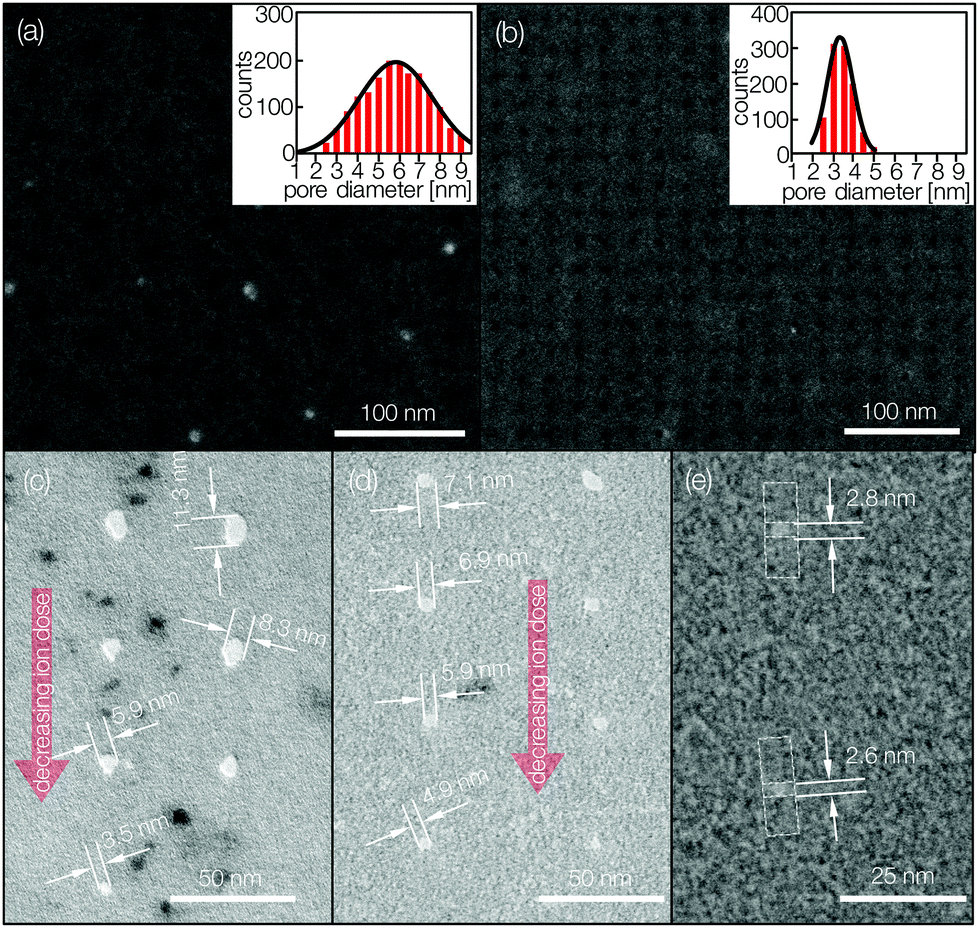 | ||
| Fig. 4 Pore arrays on graphene perforated via FIB milling. Secondary-electron-detection-mode SEM images of pore arrays having 50 nm wide (a) and 25 nm wide (b) pitches on freestanding double layer graphene perforated by 30 keV Ga+ at ∼104 per pore (a) and by 30 keV He+ at ∼4.4 × 10⁵ per pore (b), respectively. Dark contrast indicates pores. The resultant pore-size distributions are 5.9 ± 3.6 nm (a) and very narrow, 3.3 ± 1.2 nm (b). (c) Transmission-electron-mode (bright field) SEM image of pores on freestanding monolayer graphene perforated by 30 keV Ga+ at 2500 × 104 per pore (bottom to top), exhibiting pore sizes from 3.5 to 11.3 nm. (d, e) Transmission-electron-mode (bright field) SEM images of pores on the monolayer graphene perforated by 30 keV He+ at 3.9–6.2 × 10⁵ per pore (d, bottom to top) and 2.7 × 10⁵ He+ per pore (e), showing pore sizes of 4.9–7.1 nm (d) and 2.6 and 2.8 nm (e), respectively. | ||
The critical dimension (CD) of the FIB-drilled pores is dependent on the ion irradiation dose. In order to obtain the relationship between CD and ion dose unambiguously, we characterized the FIB perforation of a simple monolayer graphene system. When the 30 keV Ga+ irradiation dose was reduced from 104 to 7500 to 5000 to 2500 ions per pixel (or pore), the respective pore sizes measured 11.3, 8.3, 5.9 and 3.5 nm (Fig. 4c), revealing the dependency of the (monolayer) graphene CD on the ion dose. The smallest pore size obtained in this experiment is significantly smaller than the previously reported results of sub-10 nm pores on graphene.25 The tight control of the exposed ions does not only allow us to pattern at the resolution limit of the Ga+ FIB system defined by the beam size (∼4 nm). The low dose guaranties an exceptionally short process time of a few microseconds per pattern, enabling even large-scale patterning of graphene for device integration.
Note that these top-down-drilled pore sizes are significantly smaller than sputtering of bulk material could produce. In the 3D sputtering process, an incident ion collides with multiple target atoms to initiate a collision cascade within the target material. Recoiling target atoms can induce a momentum inversion of certain atoms close to the surface, resulting in an escape from the bulk phase.19 These secondary events occur in the vicinity of the incident ion spot called an interaction diameter, the reported values of which are around 20–30 nm.53,54
For ion exposure of graphene in HIM we achieved even smaller feature sizes. Here again we could overcome the previously reported interaction diameter limit of 5 nm (ref. 53) and repeatedly pattern pore arrays into freestanding double layer graphene with a mean diameter of 3.4 nm at 25 nm wide spacing using 30 keV He+ ions at 4.4 × 10⁵ per pore (Fig. 4b). The effect of the total ion dose on CD (the pore size) can be observed by exposing freestanding monolayer graphene to 3.9–6.2 × 10⁵ He+ ions per pixel, revealing again the ion dose dependency of the (monolayer) graphene CD (Fig. 4d).
Despite the single-pixel exposure we see a pore size increase from 4.9 to 7.1 nm caused by the imperfect spot shape of the irradiating beam. By decreasing the number of He+ hitting the monolayer graphene to 2.7 × 10⁵ we were able to produce holes with 2.6 nm wide diameter (Fig. 4e), comparable to pore sizes drilled in graphene using TEM systems.21,55 Our results show a significant advancement in graphene patterning via FIB milling in terms of feature size and array dimension, enabled by detailed knowledge of the interaction mechanisms involved and the 2D nature of our target material. The use of freestanding graphene allowed us to create patterns while avoiding undesirable secondary effects during FIB milling (e.g., ion implanting and substrate swelling), unlike those frequently reported for the supported graphene samples.13,15,35,56
Conclusions
Experimental and theoretical investigations of the interaction between freestanding graphene layers and energetic ion irradiation confirm that pristine graphene could be transparent to materials at elevated kinetic energy, suggested by previous theoretical investigations.17 For instance, graphene is highly transparent to 30 keV-accelerated He+ particles, only ∼1% of which collide with the graphene lattice and sputter carbon atoms as compared with 47% for Ga+ (30 keV). Both binary collision theory and experimental characterization point out the uniqueness of 2D material sputtering in that the major sputtering mechanism would be a simple binary collision between the incident ion particle and the carbon atom in the lattice, in clear contrast to vibration energy cascade and recoiling for 3D material sputtering and also in contrast to the DFT theory predictions on the multilayer effect. These findings represent a simple understanding of ballistic ion collisions with 2D materials and permit the prediction of an actual sputter yield of atomically thin targets, which has not been possible with other techniques. The sputtering probability (i.e., sputter yield) of the freestanding graphene layers depends strongly on the species and kinetic energies of the bombarding ion particles, as well as on the number of layers. These findings lead altogether to a rationale for the 2D material patterning such that precise control of the local ion irradiation dose on freestanding 2D materials could bring the size limit of this technology to a new level. This pattern generation strategy was firstly attested by the creation of hole-array patterns with feature sizes down to 2.6 nm and 3.5 nm using He+ FIB and Ga+ FIB, respectively. These results highlight the great potential of efficient, sub-5 nm scale feature generation on 2D materials and thereby close the gap between theory verification and pore-array-patterning practice, opening up great possibilities in the nanomanufacture of devices that use flexible 2D materials patterned on a nanometer scale.Acknowledgements
We appreciate the support from Binnig and Rohrer Nanotechnology Center of ETH Zurich and IBM Zurich. J.B. thanks the Swiss National Science Foundation for financial support (200021-137964). I.S. is grateful to the Swiss National Science Foundation for support in equipment procurement (REquip 206021-133823). This work was partially supported by LG Electronics Advanced Research Institute, for which R.M.W. is thankful. I.S. thanks Y. Zheng at EMPA (Swiss Federal Laboratories for Materials Science and Technology), Switzerland, for his initial contribution to the perforated graphene imaging.References
- K. S. Novoselov, V. I. Fal'ko, L. Colombo, P. R. Gellert, M. G. Schwab and K. Kim, Nature, 2012, 490, 192–200 CrossRef CAS PubMed.
- C. Lee, X. Wei, J. W. Kysar and J. Hone, Science, 2008, 321, 385–388 CrossRef CAS PubMed.
- K. S. Novoselov, A. K. Geim, S. V. Morozov, D. Jiang, Y. Zhang, S. V. Dubonos, I. V. Grigorieva and A. A. Firsov, Science, 2004, 306, 666–669 CrossRef CAS PubMed.
- A. A. Balandin, S. Ghosh, W. Bao, I. Calizo, D. Teweldebrhan, F. Miao and C. N. Lau, Nano Lett., 2008, 8, 902–907 CrossRef CAS PubMed.
- R. R. Nair, P. Blake, A. N. Grigorenko, K. S. Novoselov, T. J. Booth, T. Stauber, N. M. Peres and A. K. Geim, Science, 2008, 320, 1308 CrossRef CAS PubMed.
- J. S. Bunch, S. S. Verbridge, J. S. Alden, A. M. van der Zande, J. M. Parpia, H. G. Craighead and P. L. McEuen, Nano Lett., 2008, 8, 2458–2462 CrossRef CAS PubMed.
- K. Celebi, J. Buchheim, R. M. Wyss, A. Droudian, P. Gasser, I. Shorubalko, J. I. Kye, C. Lee and H. G. Park, Science, 2014, 344, 289–292 CrossRef CAS PubMed.
- L. Peng, X. Peng, B. Liu, C. Wu, Y. Xie and G. Yu, Nano Lett., 2013, 13, 2151–2157 CrossRef CAS PubMed.
- X. Li, W. Cai, J. An, S. Kim, J. Nah, D. Yang, R. Piner, A. Velamakanni, I. Jung, E. Tutuc, S. K. Banerjee, L. Colombo and R. S. Ruoff, Science, 2009, 324, 1312–1314 CrossRef CAS PubMed.
- S. Bae, H. Kim, Y. Lee, X. Xu, J. S. Park, Y. Zheng, J. Balakrishnan, T. Lei, H. R. Kim, Y. I. Song, Y. J. Kim, K. S. Kim, B. Ozyilmaz, J. H. Ahn, B. H. Hong and S. Iijima, Nat. Nanotechnol., 2010, 5, 574–578 CrossRef CAS PubMed.
- T. Gokus, R. R. Nair, A. Bonetti, M. Bohmler, A. Lombardo, K. S. Novoselov, A. K. Geim, A. C. Ferrari and A. Hartschuh, ACS Nano, 2009, 3, 3963–3968 CrossRef CAS PubMed.
- J. H. Chen, W. G. Cullen, C. Jang, M. S. Fuhrer and E. D. Williams, Phys. Rev. Lett., 2009, 102, 236805 CrossRef PubMed.
- M. C. Lemme, D. C. Bell, J. R. Williams, L. A. Stern, B. W. Baugher, P. Jarillo-Herrero and C. M. Marcus, ACS Nano, 2009, 3, 2674–2676 CrossRef CAS PubMed.
- B. S. Archanjo, A. P. Barboza, B. R. Neves, L. M. Malard, E. H. Ferreira, J. C. Brant, E. S. Alves, F. Plentz, V. Carozo, B. Fragneaud, I. O. Maciel, C. M. Almeida, A. Jorio and C. A. Achete, Nanotechnology, 2012, 23, 255305 CrossRef CAS PubMed.
- A. N. Abbas, G. Liu, B. Liu, L. Zhang, H. Liu, D. Ohlberg, W. Wu and C. Zhou, ACS Nano, 2014, 8, 1538–1546 CrossRef CAS PubMed.
- G. Nanda, S. Goswami, K. Watanabe, T. Taniguchi and P. F. Alkemade, Nano Lett., 2015, 15, 4006–4012 CrossRef CAS PubMed.
- O. Lehtinen, J. Kotakoski, A. V. Krasheninnikov, A. Tolvanen, K. Nordlund and J. Keinonen, Phys. Rev. B: Condens. Matter, 2010, 81, 153401 CrossRef.
- O. Lehtinen, J. Kotakoski, A. V. Krasheninnikov and J. Keinonen, Nanotechnology, 2011, 22, 175306 CrossRef CAS PubMed.
- J. F. Ziegler, J. P. Biersack and U. Littmark, The Stopping and Range of Ions in Solids, Pergamon Press, 1985 Search PubMed.
- D. C. Bell, M. C. Lemme, L. A. Stern, J. R. Williams and C. M. Marcus, Nanotechnology, 2009, 20, 455301 CrossRef CAS PubMed.
- M. D. Fischbein and M. Drndic, Appl. Phys. Lett., 2008, 93, 113107 CrossRef.
- A. W. Robertson, C. S. Allen, Y. A. Wu, K. He, J. Olivier, J. Neethling, A. I. Kirkland and J. H. Warner, Nat. Commun., 2012, 3, 11440 Search PubMed.
- J. Bai, J. Bai, X. Zhong, X. Zhong, S. Jiang, S. Jiang, Y. Huang, Y. Huang, X. Duan and X. Duan, Nat. Nanotechnol., 2010, 5, 190–194 CrossRef CAS PubMed.
- S.-S. Kim, M. J. Park, J.-H. Kim, G. Ahn, S. Ryu, B. H. Hong and B.-H. Sohn, Chem. Mater., 2015, 27, 7003–7010 CrossRef CAS.
- A. Hemamouche, A. Morin, E. Bourhis, B. Toury, E. Tarnaud, J. Mathe, P. Guegan, A. Madouri, X. Lafosse, C. Ulysse, S. Gullet, G. Patriarche, L. Auvray, F. Montel, Q. Wilmart, B. Placais, J. Yates and J. Gierak, Microelectron. Eng., 2014, 121, 87–91 CrossRef CAS.
- D. Pickard and L. Scipioni, Zeiss application note, 2009 Search PubMed.
- D. Lucot, J. Gierak, A. Ouerghi, E. Bourhis, G. Faini and D. Mailly, Microelectron. Eng., 2009, 86, 882–884 CrossRef CAS.
- E. H. Åhlgren, J. Kotakoski and A. V. Krasheninnikov, Phys. Rev. B: Condens. Matter, 2011, 83, 115424 CrossRef.
- J. Kotakoski, C. Brand, Y. Lilach, O. Cheshnovsky, C. Mangler, M. Arndt and J. C. Meyer, Nano Lett., 2015, 15, 5944–5949 CrossRef CAS PubMed.
- K. Celebi, M. T. Cole, J. W. Choi, F. Wyczisk, P. Legagneux, N. Rupesinghe, J. Robertson, K. B. Teo and H. G. Park, Nano Lett., 2013, 13, 967–974 CrossRef CAS PubMed.
- Z. Cheng, Q. Zhou, C. Wang, Q. Li, C. Wang and Y. Fang, Nano Lett., 2011, 11, 767–771 CrossRef CAS PubMed.
- S. Průša, P. Procházka, P. Bábor, T. Šikola, R. ter Veen, M. Fartmann, T. Grehl, P. Brüner, D. Roth, P. Bauer and H. H. Brongersma, Langmuir, 2015, 31, 9628–9635 CrossRef PubMed.
- D. Fox, Y. B. Zhou, A. O'Neill, S. Kumar, J. J. Wang, J. N. Coleman, G. S. Duesberg, J. F. Donegan and H. Z. Zhang, Nanotechnology, 2013, 24, 335702 CrossRef CAS PubMed.
- Y. Zhou, R. O'Connell, P. Maguire and H. Zhang, Sci. Rep., 2014, 4, 7032 CrossRef CAS PubMed.
- J. J. Lopez, F. Greer and J. R. Greer, J. Appl. Phys., 2010, 107, 104326 CrossRef.
- A. Stanishevsky, Thin Solid Films, 2001, 398, 560–565 CrossRef.
- S. Hu, M. Lozada-Hidalgo, F. C. Wang, A. Mishchenko, F. Schedin, R. R. Nair, E. W. Hill, D. W. Boukhvalov, M. I. Katsnelson, R. A. W. Dryfe, I. V. Grigorieva, H. A. Wu and A. K. Geim, Nature, 2014, 516, 227–230 CrossRef CAS PubMed.
- S. Mathew, T. K. Chan, D. Zhan, K. Gopinadhan, A. R. Barman, M. B. H. Breese, S. Dhar, Z. X. Shen, T. Venkatesan and J. T. L. Thong, Carbon, 2011, 49, 1720–1726 CrossRef CAS.
- G. C. Maitland, M. Rigby, E. B. Smith and W. A. Wakeham, Intermolecular Forces: Their Origin and Determination, Clarendon Press, 1981 Search PubMed.
- J. Burgdörfer, Atomic Collisions with Surfaces, World Scientific Publishing, 1993 Search PubMed.
- J. Zubeltzu, A. Chuvilin, F. Corsetti, A. Zurutuza and E. Artacho, Phys. Rev. B: Condens. Matter, 2013, 88, 245407 CrossRef.
- A. V. Krasheninnikov, F. Banhart, J. X. Li, A. S. Foster and R. M. Nieminen, Phys. Rev. B: Condens. Matter, 2005, 72, 125428 CrossRef.
- A. Zobelli, A. Gloter, C. P. Ewels, G. Seifert and C. Colliex, Phys. Rev. B: Condens. Matter, 2007, 75, 245402 CrossRef.
- F. Banhart, J. Kotakoski and A. V. Krasheninnikov, ACS Nano, 2011, 5, 26–41 CrossRef CAS PubMed.
- R. H. Telling, C. P. Ewels, A. A. El-Barbary and M. I. Heggie, Nat. Mater., 2003, 2, 333–337 CrossRef CAS PubMed.
- C. P. Ewels, R. H. Telling, A. A. El-Barbary, M. I. Heggie and P. R. Briddon, Phys. Rev. Lett., 2003, 91, 025505 CrossRef CAS PubMed.
- A. C. Ferrari and D. M. Basko, Nat. Nanotechnol., 2013, 8, 235–246 CrossRef CAS PubMed.
- A. C. Ferrari, J. C. Meyer, V. Scardaci, C. Casiraghi, M. Lazzeri, F. Mauri, S. Piscanec, D. Jiang, K. S. Novoselov, S. Roth and A. K. Geim, Phys. Rev. Lett., 2006, 97, 187401 CrossRef CAS PubMed.
- M. M. Lucchese, F. Stavale, E. H. M. Ferreira, C. Vilani, M. V. O. Moutinho, R. B. Capaz, C. A. Achete and A. Jorio, Carbon, 2010, 48, 1592–1597 CrossRef CAS.
- F. Tuinstra and J. L. Koenig, J. Chem. Phys., 1970, 53, 1126–1130 CrossRef CAS.
- A. Eckmann, A. Felten, A. Mishchenko, L. Britnell, R. Krupke, K. S. Novoselov and C. Casiraghi, Nano Lett., 2012, 12, 3925–3930 CrossRef CAS PubMed.
- A. Eckmann, A. Felten, I. Verzhbitskiy, R. Davey and C. Casiraghi, Phys. Rev. B: Condens. Matter, 2013, 88, 035426 CrossRef.
- M. Ananth, L. Stern, D. Ferranti, C. Huynh, J. Notte, L. Scipioni, C. Sanford and B. Thompson, Scanning Microscopies 2011: Advanced Microscopy Technologies for Defense, Homeland Security, Forensic, Life, Environmental, and Industrial Sciences, 2011, vol. 8036, p. 80360M Search PubMed.
- C. J. Lo, T. Aref and A. Bezryadin, Nanotechnology, 2006, 17, 3264–3267 CrossRef CAS.
- G. F. Schneider, Q. Xu, S. Hage, S. Luik, J. N. H. Spoor, S. Malladi, H. Zandbergen and C. Dekker, Nat. Commun., 2013, 4, 2619 Search PubMed.
- S. J. Hang, Z. Moktadir and H. Mizuta, Carbon, 2014, 72, 233–241 CrossRef CAS.
Footnote |
| † Electronic supplementary information (ESI) available. See DOI: 10.1039/c6nr00154h |
| This journal is © The Royal Society of Chemistry 2016 |