
 Open Access Article
 This Open Access Article is licensed under a Creative Commons Attribution-Non Commercial 3.0 Unported Licence
Dual emission in asymmetric “giant” PbS/CdS/CdS core/shell/shell quantum dots†
Haiguang
Zhao
*ab,
Gianluca
Sirigu
c,
Andrea
Parisini
d,
Andrea
Camellini
c,
Giuseppe
Nicotra
e,
Federico
Rosei
*bfg,
Vittorio
Morandi
d,
Margherita
Zavelani-Rossi
h and
Alberto
Vomiero
*bi
aCNR-INO SENSOR Lab, Via Branze 45, 25123 Brescia, Italy
bInstitut National de la Recherche Scientifique, 1650 Boulevard Lionel-Boulet, Varennes, Québec J3X 1S2, Canada. E-mail: rosei@emt.inrs.ca; haiguang.zhao@emt.inrs.ca
cDipartimento di Fisica, Politecnico di Milano, piazza L. da Vinci 32, 20133 Milano, Italy
dCNR-IMM Sezione di Bologna, Via Gobetti 101, 40129 Bologna, Italy
eCNR-IMM Sezione di Catania, Strada VIII, 5, 95121 Catania, Italy
fInstitute for Fundamental and Frontier Science University of Electronic Science and Technology of China, Chengdu 610054, P.R. China
gCenter for Self-Assembled Chemical Structures, McGill University, 801 Sherbrooke Street West, Montreal, QC H3A 0B8, Canada
hDipartimento di Energia, IFN-CNR, Politecnico di Milano, via Ponzio 34/3, 20133 Milano, Italy
iDepartment of Engineering Sciences and Mathematics, Luleå University of Technology, 971 98 Luleå, Sweden. E-mail: alberto.vomiero@ltu.se
First published on 15th January 2016
Abstract
Semiconducting nanocrystals optically active in the infrared region of the electromagnetic spectrum enable exciting avenues in fundamental research and novel applications compatible with the infrared transparency windows of biosystems such as chemical and biological optical sensing, including nanoscale thermometry. In this context, quantum dots (QDs) with double color emission may represent ultra-accurate and self-calibrating nanosystems. We present the synthesis of giant core/shell/shell asymmetric QDs having a PbS/CdS zinc blende (Zb)/CdS wurtzite (Wz) structure with double color emission close to the near-infrared (NIR) region. We show that the double emission depends on the excitation condition and analyze the electron–hole distribution responsible for the independent and simultaneous radiative exciton recombination in the PbS core and in the CdS Wz shell, respectively. These results highlight the importance of the driving force leading to preferential crystal growth in asymmetric QDs, and provide a pathway for the rational control of the synthesis of double color emitting giant QDs, leading to the effective exploitation of visible/NIR transparency windows.
1. Introduction
Colloidal quantum dots (QDs) are very attractive nanoscale systems due to the possibility of controlling their optical and electronic properties by tuning their size and shape.1–3 Such systems have already demonstrated their potential in various applications, including light-emitting diodes, photodetectors, excitonic solar cells, biomedical labeling, nanothermometers and photocatalysis.4–10Recent studies demonstrated that the formation of a core/shell structure can largely enhance the chemical, thermal, and photochemical stability of QDs, thanks to the ability of the shell to passivate the core, by removing defects/traps, preserving it from oxidation. Improved functional properties of devices based on core/thin shell QDs have been recently demonstrated, thanks to the passivation of the external shell, which guarantees enhanced charge lifetime and improved stability of the core/shell system.11–13
The optical and electronic properties of the QDs are found to be significantly different in core/shell structures.14–17 In general, in core/shell QDs, the shell influences the charge distribution and acts as a protective layer for the core, keeping it away from the surface interactions and the surrounding environment.10,14–16,18 In most cases, the shell does not emit light due to core/shell level alignment and charge relaxation or due to the ultrafast non-radiative Auger recombination of the exciton after excitation.14,16,17,19 In a few very recent cases core/shell systems were shown to exhibit double emission, due to fluorescence,16,20–23 amplified spontaneous emission24 and laser emission25 originating from distinct core and shell radiative recombination. Double emission was also reported in CdSe/CdS core/shell tetrapods due to a spatially direct transition in the core and a spatially indirect emission across the CdSe/CdS heterojunction.20 In core/shell/shell quantum systems, double emission is obtained by the extra energy barrier of the inner shell between the core and the external shell, which inhibits charge transfer.26–28 For example, Peng et al. demonstrated double color emission in the CdSe/ZnS/CdSe core/shell/shell QDs originating from the CdSe core and the CdSe shell, respectively.26 An analogous phenomenon was reported in chunky rod-shaped Te-doped CdSe/CdS/CdZnSe core/shell/shell nanostructures.27 A similar effect was found in “dot-in-bulk” CdSe/CdS nanocrystals, in which the thin layer of zinc blende (Zb) phase CdS, sandwiched between the core and the thick wurtzite (Wz) CdS shell, is thought to act as the barrier.21,29 In almost all the double color emission QDs, the geometric structure is assumed to be quasi-spherical, the core occupying the geometric center of the dot, even though a systematic structural investigation is still lacking.
A special case in the frame of the core/shell systems is represented by the so-called “giant” core/shell structures, in which a relatively thick shell (shell thickness up to tens of nm) surrounds a small core exhibiting quantized electronic properties. Compared to thin shell systems, the “giant” shell can be optically active (as opposed to thin shell systems) and can be involved in processes like photoluminescence (PL), contributing significantly to the optical “fingerprint” of the “giant” core/shell system. Double emission in quantum confined “giant” core/shell systems is a very important property because they typically exhibit very good chemical and photostability toward photobleaching (in particular, suppression of photobleaching under continuous laser excitation has been demonstrated over periods of several hours repeated for several days30), so it is possible to exploit these double color materials for end-user applications in biology and optoelectronics including, for example, self-calibrating and highly accurate ratiometric probes to measure the intracellular temperature.21,29
In the panorama of QDs, increasing interest is devoted to lead chalcogenide systems, which are optically active in the near infrared (NIR) region. These kinds of QDs have great potential for use in several applications, like bio-sensors and bio-imaging, due to the deep tissue penetration of light in their emission range and their long PL lifetime (in the microsecond range), which is significantly different from the lifetime of biological tissue (∼ns). Dual emission giant NIR QDs will allow the detection of bio-local pH or temperature through the ratiometric emission probe with super photostability, which is impossible in single emission QDs or dual emission-visible QDs. In simple core/shell PbS/CdS QDs double emission has been reported in very few cases.16,21 In these QDs the long wavelength emission was attributed to the PbS core and the short wavelength was assigned to trap emission of the CdS shell. However, this trap-related emission is highly unstable: such instability makes it almost impossible to precisely control the double emission, and inhibits any possible exploitation for practical applications. In addition, bandgap emission from the shell is very hard to achieve and has never been reported in NIR core/shell systems, due to the presence of traps after long time/high temperature cation exchange reaction.
Here we report double color emission in “giant” PbS/CdS/CdS core/shell/shell asymmetric QDs optically active in the visible and close to NIR region, and describe the effect that underpins the double peak fluorescence. The “giant” QDs are synthesized through a successive ionic layer absorption and reaction (SILAR) technique, which allows us to coat the PbS pure QD with a CdS shell of variable thickness (Fig. 1). For shells thicker than 3.5 nm, QDs begin to exhibit two distinct PL peaks, associated with the quantum confined PbS core and the CdS shell states. We clearly identified an anisotropic growth of the QDs leading to an optically active PbS core, a tetrahedrally shaped Zb shell and a further asymmetric Wz shell responsible for emission. Zb and Wz shells exhibit precise crystallographic orientation relationships leading to the formation of strongly asymmetric QDs with Wz nanograins growing on some of the tetrahedron {111} faces of the inner CdS shell. By using ultrafast pump–probe spectroscopy and high resolution transmission electron microscopy (HR-TEM) we provide evidence of electron delocalization and of the presence of a Zb CdS layer between the PbS core and the Wz CdS shell. Electron delocalization and blocking of the hole relaxation towards the core21,24 give rise to direct radiative recombination in the CdS shell.
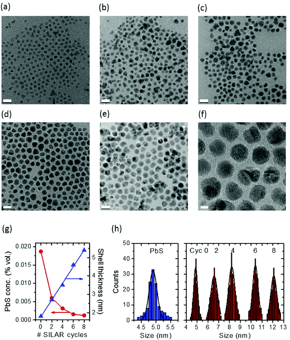 | ||
| Fig. 1 Size and size distribution of giant QDs. (a)–(f): TEM. (a) Representative TEM images of parent PbS/CdS QDs after cation exchange, before SILAR. (b)–(f): PbS/CdS QDs after coating with 2 (b), 4 (c), 6 (d) and 8 (e) SILAR cycles. (f) HR-TEM image of sample (e). Scale bar is 20 nm in (a)–(e) and 5 nm in (f). (g) Overall shell thickness and Pb volume concentration as a function of the number of SILAR cycles. (h) Size distribution of parent PbS QDs before cation exchange (blue) and of the core/shell QDs after different SILAR cycles. The solid lines are Gaussian fits of the experimental data. | ||
2. Experimental
2.1 Materials
Lead chloride (98%), sulfur (100%), oleylamine (OLA) (technical grade, 70%), cadmium oxide (99%), oleic acid (OA), cardiogreen (IR 125), rhodamine 6G and octadecene (ODE) were obtained from Sigma-Aldrich Inc. Hexane, toluene, dimethyl sulfoxide and ethanol were purchased from Fisher Scientific Company. All chemicals were used as purchased.2.2 Synthesis
PbS/CdS QDs with a thick shell were synthesized via a two-step cation exchange procedure.16 In the first step, a thin shell was synthesized as described above. Without any purification, the reaction temperature was further increased to 240 °C and the reaction was allowed to proceed for 2 hours. The reaction was quenched by injection of cold toluene (−20 °C). Ethanol was added, and then the suspension was centrifuged and supernatant was removed. The QDs were dispersed in toluene.
2.3 Structural and optical characterization
The morphology of PbS/CdS QDs was determined using a JEOL 2100F transmission electron microscope (TEM). TEM as well as scanning transmission electron microscopy (STEM) investigations were also performed with a FEI Tecnai F20 ST TEM/STEM equipped with a high angle annular dark field (HAADF) STEM detector and an energy dispersive X-ray spectrometer (EDS). Both microscopes were operated at 200 keV. The Pb/Cd ratio was measured by using inductively coupled plasma optical emission spectrometry (ICP-OES) (Perkin Elmer Model Optima 7300 DV). The small angle XRD study of extensively purified PbS or PbS/CdS QDs was carried out with a Philips X'pert diffractometer using a Cu Kα radiation source (λ = 0.15418 nm).The absorption spectra were acquired with a Cary 5000 UV-Vis-NIR spectrophotometer (Varian) with a scan speed of 600 nm min−1. Fluorescence spectra were obtained with a Fluorolog®-3 system (Horiba Jobin Yvon).
The PL lifetime of PbS cores in QDs in toluene was measured using a pulsed laser diode of 444 nm and fast multichannel scaler mode in the Fluorolog®-3 system. The PL lifetime of the CdS shell was measured in the time-correlated single-photon counting (TCSPC) mode with a 444 nm laser.
QY measurements for PbS or PbS/CdS/CdS QDs were carried out using Dye IR 125 as a reference. The QY of CdS shell was measured by using rhodamine 6G as a reference.
Transient transmission ΔT/T measurements were carried out by the pump–probe technique. We used a regeneratively-amplified Ti:Sapphire laser system delivering pulses with 150 fs duration, 500 μJ energy, at 1 kHz repetition rate and 800 nm central wavelength. More details are described in the ESI.†
3. Results and discussion
3.1 Synthesis and structure of PbS/CdS/CdS core/shell/shell QDs
PbS QDs were first synthesized according to procedures found in the literature, and were subsequently used to grow a shell via the cation exchange approach.15,16 Subsequently, a thick CdS shell was grown by a successive ionic layer absorption and reaction (SILAR) method at 240 °C under N2 flow, similar to the reported approach for the synthesis of visible/NIR giant PbSe/CdSe/CdS QDs.31,32 So in the present study, a two-step cation exchange was used, followed by SILAR. First, we induce the growth of a thin CdS shell at low temperature, T1 and then the growth of a thicker CdS shell at a higher temperature T2 (T2> T1). By using this approach we stabilize the PbS core during high-temperature processing.16 During this process, the overall size of QDs does not change (see Fig. 1h, the blue histogram and the red histogram corresponding to Cyc 0). The as-synthesized CdS shell provides a strong protection to the PbS core against the Ostwald ripening during SILAR and allows us to attain “giant” PbS/CdS/CdS core/shell/shell (asymmetric) QDs with reasonably uniform particle size and morphology at high temperatures (as high as 240 °C) (Fig. 1).30Unlike the giant NIR InP/CdS QDs,30 it was found that the growth of SILAR CdS shells on the as-synthesized pure PbS/CdS QDs is very sensitive to the reaction temperature. In this respect, we carried out SILAR growth of the CdS shell at temperatures as low as 200 °C, to investigate the final shape of the crystals as a function of the growth temperature. Typically, at 240 °C, SILAR growth results in the presence of different grains inside the observed nanoparticles, and hexagonal and distorted polygonal projected shapes are found after 8 cycles (see Fig. 1f). Triangular, rectangular and rhombic projected shapes are found in nanostructures, when adding a SILAR precursor at 200 °C, as shown in Fig. S1a and b,† consistent with the previous reports for “giant” PbSe/CdSe/CdS QDs,33 because the precursor may only grow along a preferential crystallographic direction. This may be entirely attributed to the kinetics of Cd and S atom deposition.31 At higher temperature (240 °C), crystal growth becomes less preferentially oriented. If the protective shell produced by cation exchange is not thick enough (thinner than 1.0 nm), Ostwald ripening of PbS QDs occurs during SILAR, giving rise to very broad QD size distributions and leading to a complete loss of the PL signal.16
The starting PbS/CdS core/shell QDs after the cation exchange (Cyc 0) have a PbS core diameter of ∼1.2 nm and a CdS shell 1.7 nm thick. These values are obtained by considering the Pb/Cd molar ratio obtained by ICP-OES and the overall particle size as obtained by TEM, according to the procedure described in ref. 16. We produced different SILAR cycles, and the TEM analysis (Fig. 1a–e and Table 1) reveals the linear increase of QD size. After 8 cycles (sample Cyc 8), the final diameter of the “giant” QDs was 12.1 ± 0.5 nm, with an overall shell thickness of around 5.4 ± 0.5 nm (Table 1). The PbS core size after SILAR in Table 1 was calculated by taking into account the Pb/Cd molar ratio obtained by ICP-OES before SILAR (Cyc 0), under the hypothesis that the PbS core does not shrink during SILAR. To confirm this hypothesis, the correct evaluation of the core size and the presence of Pb in the final QDs, we carried out ICP-OES after SILAR in the Cyc 8 sample. Pb was clearly detected in the spectra. We re-calculated the expected core size and shell thickness for these samples and we compared the results with the estimate obtained from the Pb/Cd molar ratio before SILAR and under the hypothesis of no-shrinking of the core during SILAR. The results are reported in Table S1† and demonstrate a good agreement of the estimate before and after SILAR and confirm the hypothesis that the PbS core does not shrink during the growth of the shell.
| Sample | Overall size (nm) | Core size (nm) | Shell thickness (nm) | Lifetime (ns) @480 nm | Lifetime (ns) @690 nm |
|---|---|---|---|---|---|
| PbS | 4.9 ± 0.2 | 4.9 | 0 | — | — |
| Cyc0 | 4.9 ± 0.3 | 1.2 | 1.8 | — | 1130 ± 30 |
| Cyc2 | 6.6 ± 0.7 | 1.2 | 2.7 | — | 1180 ± 30 |
| Cyc4 | 8.2 ± 0.5 | 1.2 | 3.5 | 13 ± 1 | 1190 ± 30 |
| Cyc6 | 10.4 ± 0.4 | 1.2 | 4.6 | 16 ± 1 | 1150 ± 30 |
| Cyc8 | 12.1 ± 0.5 | 1.2 | 5.4 | 17 ± 1 | 1140 ± 30 |
XRD (Fig. 2) illustrates the structural evolution of the QDs during shell growth. PbS QD exhibits a rock-salt structure, as expected. The core/shell nanocrystals after cation exchange (0 cyc) show a Zb CdS-like pattern. The XRD pattern of the PbS core is still present, but difficult to detect, due to the very small PbS content (1.8% by volume, see Fig. 1g), which is close to the detection limit. After 2 cycles of CdS SILAR coating, new reflections appear, due to the CdS hexagonal Wz structure, which overlaps with the Zb. After 8 cycles of CdS coating, the PbS pattern almost completely disappears (PbS content is 0.1% in vol) and the overall diffraction pattern is dominated by the two-phase crystal structure with hexagonal Wz and Zb structures (Fig. 2). The obtained core/shell/shell QDs are inherently asymmetric, as demonstrated below.
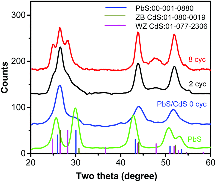 | ||
| Fig. 2 Structural evolution of the giant QD during the synthesis. XRD patterns of parent PbS (∼4.9 nm in diameter, green) and PbS/CdS QDs after cation exchange (0 cyc, blue), and after SILAR coating with 2 (black) and 8 (red) cycles. The JCPDS card files for PbS (001-0880, blue line) and CdS (01 080 0019, black for zinc blende and 01-077-2306, magenta for wurtzite) are shown for identification. | ||
To confirm these results and gain deeper insight into the observed structural modifications, we performed a detailed high-resolution electron microscopy (HREM) investigation of the QD structural evolution after different SILAR cycles. The results of this investigation are summarized in Fig. 3 (and in Fig. S1c, S2 and S3 of the ESI†). In the HREM micrograph reported in Fig. 3a, obtained from a sample after 8 SILAR cycles, two typical QDs are observed along a [110] Zb zone axis. The presence of two distinct CdS phases, i.e. the cubic Zb and the hexagonal Wz, is observed, thus confirming previous XRD findings (see also Fig. S3†). However, the structure of these QDs appears to be ruled by precise crystallographic orientation relationships between the two CdS phases leading to a shape that can be hardly described by a simple core/shell/shell spherical model. In both particles observed in Fig. 3a, two Wz grains appear to have grown on the {111}Zb planes of a central Zb grain. The crystallographic orientation relationship between the two CdS phases is as follows:
〈![[1 with combining macron]](https://www.rsc.org/images/entities/char_0031_0304.gif) 1〉Zb||〈0002〉Wz
1〉Zb||〈0002〉Wz
〈220〉Zb||〈20〉Wz
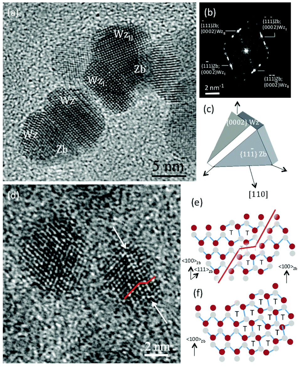 | ||
| Fig. 3 HREM investigation of the modifications of the PbS/CdS/CdS QDs structure after different SILAR cycles. (a) and (d) HREM micrographs of QDs after 8 and 0 SILAR cycles, respectively; (b) diffractogram taken on the upper particle visible in (a); (c) schematic representation of the shape of the particles observed in (a); (e) and (f) schemes of the atomic structure of a stacking fault (SF) in the Zb structure and of the interface between Zb and Wz phases, respectively. | ||
The former relationship has been marked for both the Wz grains in the diffractogram reported in Fig. 3b obtained on the upper particle in Fig. 3a. The projected triangular shape of the central Zb grain as well as the fact that this phase is bound by {111}Zb planes suggest a tetrahedral shape for the cubic inner particles. To confirm this, we performed HREM and high-resolution scanning transmission electron microscopy (HR-STEM) investigations of the PbS/CdS QDs before any SILAR cycles. All the QDs were found to share the CdS cubic Zb structure (see Fig. S1c and S2 in the ESI† for details).
As to the formation of the Wz phase on the {111}Zb faces of the tetrahedral particles, observed in Fig. 3a after 8 SILAR cycles, a possible nucleation mechanism is suggested by a closer HREM investigation of the structure of single QDs prior to SILAR treatment. In Fig. 3d, a stacking fault on a {111}Zb plane is observed close to one of the tetrahedron's faces. In Fig. 3e and f, schemes of the atomic structure of this defect and of the interface between Zb and Wz are reported, respectively. The experimentally observed SF structure corresponds to that of an intrinsic SF that may result from vacancy agglomeration. A comparison of the schemes in Fig. 3e and f demonstrates the similarity between the defect core and the Zb–Wz interface suggesting that this defect may be the site for the nucleation of this phase onto the {111}Zb tetrahedron's faces. Nucleation and growth of highly asymmetric QDs is very important, because QDs presenting double color emission were typically supposed to be spherical,34 and the role of asymmetry was never considered or reported in similar systems. Finally, an attempt to ascertain a difference in composition between the core and the external layers of these QDs by energy dispersive X-ray spectrometry (EDS) was not successful. In the EDS simulations reported in Fig. S4,† we show that the Pb signal should be just above the EDS detection limit only in the case where the electron beam is exactly focused above the particle core. Thus the reason why this signal is not observed is most probably due to the lack of stability of the nanoparticle under intense electron beam irradiation during the tens of seconds needed to get a spectrum with sufficient statistics (in some cases a rotation of the particles under the electron beam was observed). As detailed above, Pb detection required the use of ICP-OES.
Hetero-epitaxial nucleation occurs in the first stages of shell formation, leading to the presence of Zb CdS; subsequently the shell structure steadily switches to the hexagonal Wz, which is the typical phase for CdS growth at this temperature.21,30,32
3.2 Origin of double emission in core/shell/shell QDs
The PL spectrum of the QDs exhibits a peak at around 690 nm which is very stable as confirmed through annealing the PbS/CdS sample at 240 °C after cation exchange (before SILAR) (see Fig. S5a and b†). After the cation exchange reaction, the PL peak of the core/shell/shell QDs shifts to lower wavelengths due to the shrinking of the PbS core (the first excitonic peak shifts from 1360 nm to 690 nm, near the IR region, see Fig. 4a and S5b†).16 Further growth of the CdS shell induces enhanced absorption at wavelengths below 500 nm (see Fig. 4b). The (weak) absorption features related to the PbS core are still clearly present in the spectral range in which the PbS core is expected to be active (550–600 nm) (Fig. S5c†). PL spectra of all QDs, regardless of the shell thickness, exhibit a clear peak at around 690 nm, ascribed to radiative recombination in the PbS core, for any excitation condition. In the samples Cyc 6 and Cyc 8, another broad feature appears, centered at about 610 nm (Fig. 4c) and attributed to radiative recombination from CdS trap states that form during SILAR (see Fig. S6†).16,21 This band is clearly detected, when exciting at 430 nm, yet it is not present when the system is pumped at 520 nm (Fig. 4d). In that case, no difference is detected, and only the PL peak at 690 nm is visible in all the samples of the Cyc 0–Cyc 8 series (Fig. 4d), corroborating the hypothesis of defects linked to the CdS shell.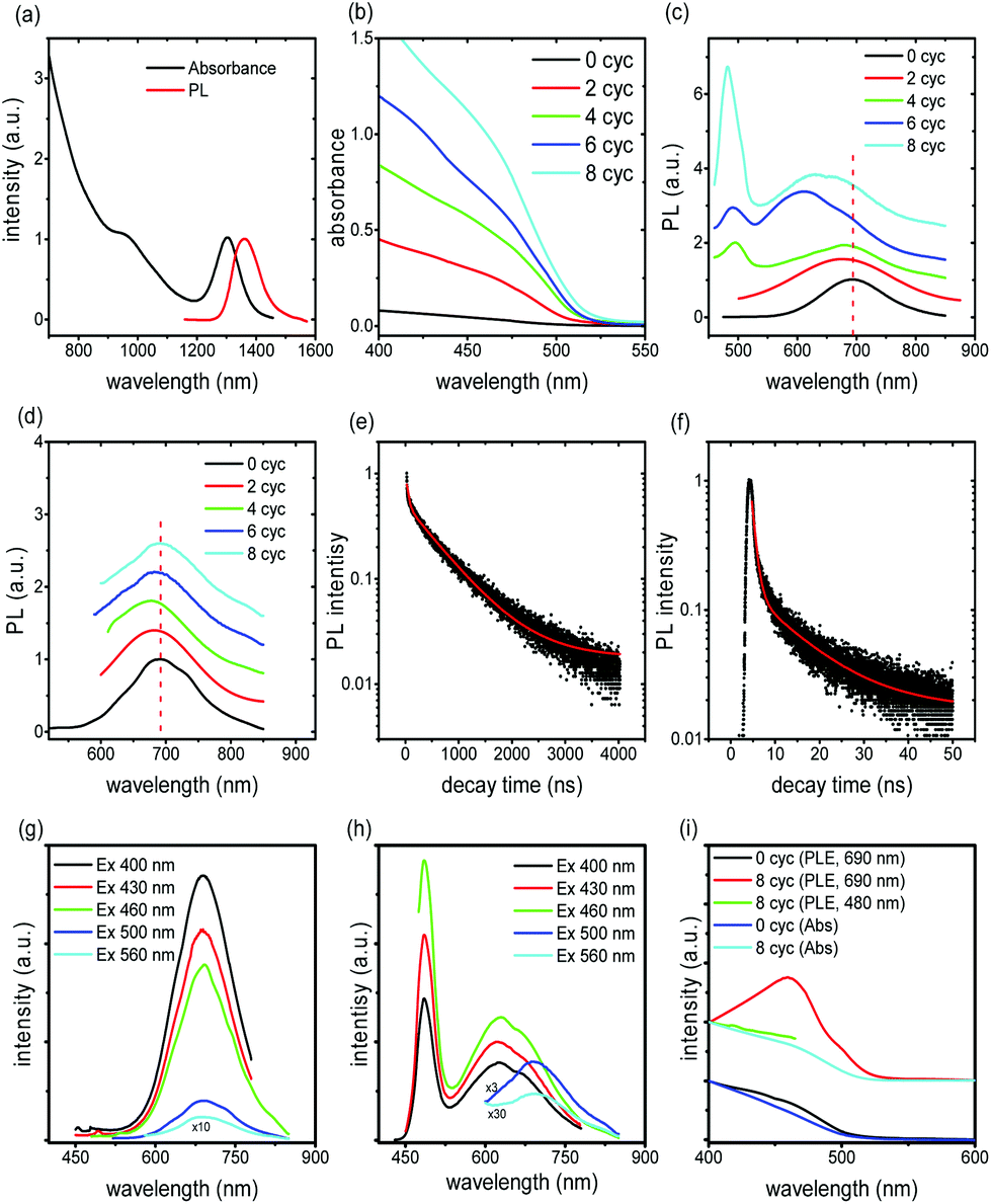 | ||
| Fig. 4 Optical properties of the giant QDs. (a) Absorption and PL spectra of the pure PbS QDs before cation exchange. Absorption (b) and PL (c and d) spectra of the PbS/CdS/CdS core/shell/shell QDs after different cycles of CdS shell growth. The excitation position is set at 430 nm in (c) and 520 nm in (d). (e) and (f): fluorescence decays of QDs in toluene for sample Cyc 8, when the emission position was fixed at (690 ± 15) nm (e) and at (480 ± 7) nm (f), respectively. The excitation wavelength is λex = 444 nm. The red curves are the fitting of the experimental data using a three-component exponential decay. The measurements were carried out at room temperature. All the samples have the same concentration for fair comparison of the relative absorption and emission intensity. PL spectra of the QDs with (g) cycle 0 and (h) cycle 8 with a tunable excitation wavelength. (i) Absorption and PLE are shown for the cycle 0 and cycle 8 samples. | ||
When pumping at 430 nm, QDs with a thick overall shell (thicker than ∼3.5 nm) exhibit two emission peaks (Fig. 4c). The PL spectrum can be well fitted using a two-component Gaussian, presenting two peaks located at 480 nm and 650 nm (Fig. S7†). This new emission peak at 480 nm is characteristic of CdS and we thus assign this PL to the recombination in the CdS shell. When the pump beam is centered at 520 nm this peak does not appear (Fig. 4d), regardless of the shell thickness. The same behaviors can be observed for various excitation wavelengths (Fig. 4g and h). We measured the PL spectra and PL excitation (PLE) spectra for samples of Cyc 0 and Cyc 8 as shown in Fig. 4g–i. The PL spectrum shows two distinct peaks when excited at 400 nm, 430 nm and 460 nm for Cyc 8, while it exhibits only one peak in Cyc 0. The PLE spectra (red and green line in Fig. 4i) of the two PL peaks of cycle 8 suggest that the long PL peak is associated with the core and the short wavelength peak is associated with the shell. The PLE of the long wavelength PL peak follows the absorption spectrum of the sample very well at the wavelength range >480 nm and shows significantly lower intensity at wavelengths <480 nm, where the absorption of the CdS resides. Instead, for Cyc 0, the PLE signal follows the absorption spectrum in the full range, without any interference of CdS absorption.
The lifetime of the two emission bands was investigated through transient PL spectrometry under excitation at λex = 444 nm, by focusing on emission at 690 nm and 480 nm (Fig. 4e and f, respectively). For all the samples, the decay curves of the PL peak centered at 690 nm of QDs are well fitted by a three-component decay. As reported in ref. 31, due to the multi-exponential nature of the PL decay in our heterostructures, it is difficult to assign a physically meaningful average lifetime based on the linear combination of an arbitrary number of single-exponential decays, nevertheless we considered the results of the fitting procedure to obtain more insight in the physical processes. A detailed analysis of lifetimes of the emission bands at 480 nm and 690 nm is reported in Table S2.† The intensity-weighted average lifetime <τ> is estimated as reported in eqn (S1),† according to the literature.33,36 The final results are reported in Table 1.
We focus first on the emission at around 690 nm. The lifetime of this band is around (1.12 ± 0.03) μs for sample Cyc 0, in agreement with the previously reported data for PbS QDs.16,22,35–37 The long lifetime component (1.3–1.7 μs) corresponds to the typical values for PbS nanocrystals with the effects of dielectric screening,37–40 and it can be thus assigned to radiative recombination through the PbS bandgap. The shorter lifetime component (in the range 40–100 ns) cannot be easily attributed, as extensively reported in previous work.37–40 The lifetime component of the order of several hundred nanoseconds may be due to the contribution from CdS trap-related radiative recombination, possibly also responsible for the band at around 610 nm in Cyc 6 and Cyc 8 samples, in very good agreement with a very recent paper on double-emission CdS QDs (see Fig. S6†).41 This strengthens the assignment of trap bands at around 610 nm. All the core/shell/shell QDs show a reduction in both the average lifetime and in the longest component of the lifetime with respect to the pure PbS QDs, most probably due to the increased contribution of non-radiative recombination because of the presence of traps/defects forming during shell growth.41,42 This conclusion is consistent with the reduction of QY during the SILAR process (Table S2†) and with analogous results in the literature.31 The decrease in QYs induced by SILAR implies that PL decay is dominated by non-radiative processes. Bearing all considerations in mind we can finally conclude that the emission at long wavelengths is due to long living radiative recombination in PbS dots, with a short living contribution from CdS trap states.
The emission peak at 480 nm is close to the reported band gap energy of bulk Wz and Zb CdS (488 nm, and 496 nm, respectively).21,43,44 The absorption spectrum (Fig. 4b) shows a knee at about 470 nm corresponding to a quantum confined CdS. In addition, the emission peak width is very narrow (∼25–35 nm), the lifetime is well fitted by a bi-exponential decay (Fig. 4f), and yields an average lifetime of ∼(13–17) ns (see Table 1), which is in the typical range of CdS emission.45,46 The two lifetime components (around 10–18 ns and 3 ns, respectively) are within the range typically reported for CdS QDs.41,46,47 In particular, the shorter lifetime (3 ns) is attributed to the initially populated band-edge state, while the longer-lifetime (16–18 ns) is attributed to the involvement of surface states in the carrier recombination process.48 All these features suggest the attribution of the peak at 480 nm to the band edge emission of the CdS shell.
The formation of the shell induces two different processes, which affect the PL lifetime in different ways. The first is the possibility of electron delocalization through the whole QD, which would lead to an increased lifetime of radiative recombination processes, the second is the formation of traps, which implies a reduction of the lifetime through the activation of other trap-mediated relaxation processes.
To gain a clear picture of all physical processes involved in PL, we performed pump–probe experiments with ∼100 fs time resolution so as to assess directly the electron–hole dynamics in double emission QDs. We probed the visible spectral region with the pump tuned at various photon energies, chosen to selectively excite the whole system (PbS and CdS) or only the PbS and then follow the exciton dynamics. The CdS bandgap, as mentioned above, is at around 2.64 eV (470 nm). The assignment of the bandgap of the PbS is not as trivial for giant QDs, from the absorption spectrum (Fig. S5c†), as already mentioned, as we identify a PbS broad feature around (550–600 nm). To give a more precise value we cannot use semi-empirical laws, which correlate the dot size with the bandgap finely reproducing the experimental data for big dots (size larger than about 2 nm) but failing for small dots, because in this region the bandgap vs. size dependence is highly nonlinear.49,50 According to the data reported in Table 1, we have a very small PbS dot, with a size of about 1.2 nm, so we expect a large bandgap, and we can estimate its value, even if with some uncertainty, from the few experimental data reported in the literature. Using the data from ref. 40 and 50, we expect a bandgap around 2.2 eV (560 nm) with a Stokes shift of about 420 meV. This last value, in turn, is in agreement with the data reported in ref. 40 and similar Stokes shifts are also reported in ref. 51 and 52. On this basis, we can obtain insights into the level alignment between PbS and CdS by performing pump–probe experiments.
We excite the sample with different photon energies (3.1 eV–400 nm, 2.64 eV–470 nm and 2.38 eV–520 nm) and we record the differential transient transmission ΔT/T at various pump–probe delays. The main feature which appears in all ΔT/T spectra is a photo-bleaching (PB) signal at around 490 nm, which denotes the presence of excited carriers in the CdS. This PB appears irrespective of the pump wavelength (Fig. 5a and b): at high pump photon energies (higher than 2.64 eV, with the wavelength lower than 470 nm) it is due to electrons and holes directly injected in the CdS, but at low pump photon energies (lower than 2.64 eV, with the wavelength higher than 470 nm) holes are hardly promoted in CdS. In particular, with the pump tuned at 470 nm (2.64 eV), we inject electrons and holes close to the CdS bandgap, but with the pump tuned at 520 nm (2.38 eV), we excite only the PbS core, and holes cannot populate CdS states, because the valence band of CdS is at higher energies (Fig. 5e). PB in this case is thus assigned to electrons delocalized along the shell. The PB can be well fitted by a two Gaussian component curve (Fig. 5a), and considering the schematic of the energy levels of the system (Fig. 5e), we might ascribe the low wavelength component to the CdS Wz shell, and the high wavelength to the Zb layer. The PB shows a very fast rise time (200–400 fs) (Fig. 5c), a different evolution in the first picoseconds, due to electron–hole redistribution in the CdS, and a long living signal (Fig. 5d). The PB signal rises rapidly when pumping at low photon energies (2.38 eV), below the bandgap of CdS. Such a fast rise is to be correlated to an “instantaneous” population of CdS electron states, suggesting that the conduction band of the PbS and that of the CdS are almost aligned. So, even if we cannot access the exact value of the PbS bandgap and cannot quantify the confinement effect in the CdS shells, we can draw the important conclusion that the system shows a quasi-type II alignment. In Fig. 5e we sketch this, using reference parameters.
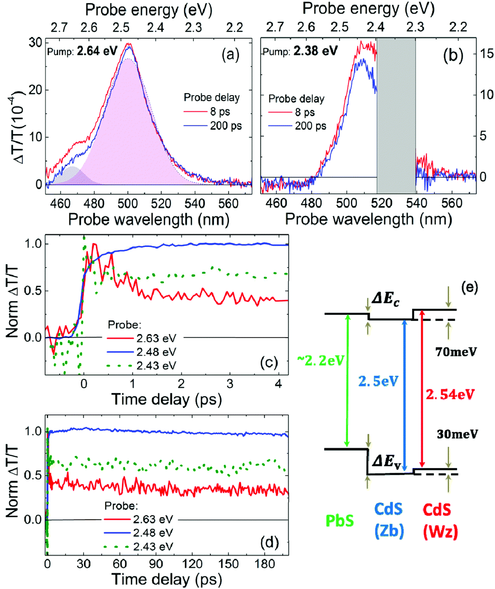 | ||
Fig. 5 ΔT/T for the Cyc 8 sample. (a, b) ΔT/T spectra at different pump–probe delays: (a) pump at 2.64 eV (470 nm), absorbed fluence of 1.3 μJ cm−2, dashed line is the fit of the blue spectrum with the two Gaussian components (violet and pink areas); (b) pump at 2.38 eV (520 nm), absorbed fluence of 1.8 μJ cm−2 (the gray region is due to scattering of the pump beam). (c, d) Corresponding normalized ΔT/T dynamics at different pump and probe wavelengths; red and blue solid line: pump at 2.64 eV (470 nm), probe at 2.63 eV (472 nm) and 2.48 eV (500 nm) respectively; green dotted line: pump at 2.38 eV (520 nm), probe at 2.43 eV (510 nm). (e) Scheme of the energy level diagram using bulk parameters for CdS Zb and Wz and for PbS data discussed in the text with inversely enlarged energy bands according to the effective masses (in m0 units 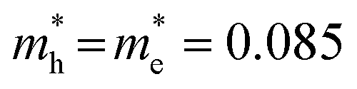 ). ). | ||
The PB signal decays (Fig. 5d) on a time scale that exceeds the time interval that we probe (200 ps), with a time constant that we estimate to be in the ns range. Such a long living feature is present for any pump photon energy and either at low or at high pump fluences (see Fig. S8 in the ESI†). This corresponds to long living excited electrons in the CdS, which can thus give rise to a PL signal at around 480 nm, by radiative recombination, when also holes are promoted in the CdS. In our picture the presence of holes in CdS is possible only if the pump photon energy is tuned to energies higher than 2.64 eV (wavelength lower than 470 nm). Nevertheless also in these conditions holes should relax in the PbS valence band. The double emission previously observed reveals that some holes decay in the PbS, giving rise to radiative recombination at around 690 nm in the PbS, and some holes remains in the CdS, giving rise to PL at around 480 nm. Such hole behavior can be ascribed to a blocking of relaxation towards the core due to a hole-blockade effect, as in dot-in-bulk CdSe/CdS QDs,21,53 that show a similar potential landscape in the valence band, or to saturation of the core transition, as in dot-in-rod CdSe/CdS QDs.24 On the other hand, when exciting with low energy pump photons (with energy below 2.64 eV and wavelength higher than 470 nm) we observe only PL from PbS, as in this case holes remains confined in the core. We can thus conclude that the scheme of Fig. 5e correctly describes the dual emission of the QDs, regardless of the uncertainty in the energy values.
In ΔT/T spectra we also observe a weak broad band of photoinduced absorption (PA), at probe wavelengths higher than 570 nm (photon energies below 2.18 nm), when the excitation is tuned at high photon energies (above 2.64 eV), with high pump fluences (Fig. S7b and d†). The PA spectrum is almost featureless, extending over all our probed region (up to 750 nm), and the signal is long lasting (over 200 ps). This signal can be ascribed to PA from defects related to the CdS shell. This is consistent with our previous observations on CdS trap states.
4. Conclusions and perspectives
In conclusion, we demonstrated double color emission in core/shell/shell asymmetric giant QDs composed of a PbS core, a CdS Zb intermediate shell and an additional CdS Wz shell. The growth of the Wz phase with precise crystallographic orientation with respect to the Zb phase leads to the formation of highly asymmetric QDs, in which the Wz phase is spatially separated from the PbS core, decreasing the probability of hole localization. We showed that the systems have a quasi-type II structure: excited electrons are delocalized throughout the QD regardless of the pump conditions and for high energy pump photons, holes partially relax in the core, and partially remains in the CdS valence band. The double PL characteristics (emission wavelengths and lifetime) together with the proposed band alignment match very well with the emission from the quantum confined PbS core (close to the NIR region) and CdS Wz (in the visible), which can take place in ultra large shells, several nanometers thick. These results pave the way to new strategies for the synthesis of double color emitting nanocrystals, based on nucleation and growth of selected crystal phases. We also demonstrated the possibility of fine tuning the electronic band structure in heterostructures active in the visible/NIR region, which regulates color emission. This approach may be applied to other heterostructured nontoxic semiconductors in a suitable temperature and composition range, such as Si, Ge, and CuInS QDs. The next steps for breakthrough developments in the field rely on the control of the interface structure between the different parts of the system: transition from single-to-double color emission QDs is possible, as proven for QDs active in the visible,21 or multi-color giant QDs can be synthesized. In addition, these results represent a major advance for practical applications in biology, biochemistry and nanothermometry,54,55 where optical detection at the nanoscale, color monitoring/modulation and control in the visible/NIR region are key challenges, as we have recently demonstrated.9Author contributions
The manuscript was written through contributions (conceptual, experimental, theoretical) of all authors. All authors have given approval to the final version of the manuscript.Conflict of interest
The authors declare no competing financial interests.Acknowledgements
F. R. acknowledges the FQRNT for funding through team projects and funding from MDEIE for an international collaboration grant in collaboration with the European Network WIROX. A. V. is thankful to the Kempe Foundation and the LTU Labbfond program for support for equipment, and to the European Union for partial salary support under contract no. 299490, MCIOF and for partial funding under contract no. 295216, IRSES. F. R. is grateful to NSERC for funding and partial salary support through an EWR Steacie Memorial Fellowship and the Alexander von Humboldt Foundation for a FW Bessel Award and Elsevier for a grant from Applied Surface Science. M. Z.-R. and G. S acknowledge financial support from Fondazione Cariplo through the project NANOCRYSLAS (grant no. 2012-0824); this work was performed in the context of the European COST Action MP1302 Nanospectroscopy.Notes and references
- A. L. Rogach, A. Eychmüller, S. G. Hickey and S. V. Kershaw, Small, 2007, 3, 536–557 CrossRef CAS PubMed.
- B. O. Dabbousi, J. Rodriguez-Viejo, F. V. Mikulec, J. R. Heine, H. Mattoussi, R. Ober, K. F. Jensen and M. G. Bawendi, J. Phys. Chem. B, 1997, 101, 9463–9475 CrossRef CAS.
- D. V. Talapin, J. S. Lee, M. V. Kovalenko and E. V. Shevchenko, Chem. Rev., 2010, 110, 389–458 CrossRef CAS PubMed.
- Y. Shirasaki, G. J. Supran, M. G. Bawendi and V. Bulovic, Nat. Photonics, 2013, 7, 13–23 CrossRef CAS.
- G. Konstantatos, I. Howard, A. Fischer, S. Hoogland, J. Clifford, E. Klem, L. Levina and E. H. Sargent, Nature, 2006, 442(7099), 180–183 CrossRef CAS PubMed.
- J. Tang, K. W. Kemp, S. Hoogland, K. S. Jeong, H. Liu, L. Levina, M. Furukawa, X. H. Wang, R. Debnath, D. K. Cha, K. W. Chou, A. Fischer, A. Amassian, J. B. Asbury and E. H. Sargent, Nat. Mater., 2011, 10, 765–771 CrossRef CAS PubMed.
- R. Weissleder, Nat. Biotechnol., 2001, 19, 316–317 CrossRef CAS PubMed.
- S. A. McDonald, G. Konstantatos, S. Zhang, P. W. Cyr, E. J. D. Klem, L. Levina and E. H. Sargent, Nat. Mater., 2005, 4, 138–142 CrossRef CAS PubMed.
- H. G. Zhao, A. Vomiero and F. Rosei, Small, 2015, 11, 5741–5746 CrossRef CAS PubMed.
- C. Wang, R. L. Thompson, P. Ohodnicki, J. Baltrus and C. Matranga, J. Mater. Chem., 2011, 21, 13452–13457 RSC.
- L.-H. Lai, L. Protesescu, M. V. Kovalenko and M. A. Loi, Phys. Chem. Chem. Phys., 2014, 16, 736–742 RSC.
- D. C. J. Neo, C. Cheng, S. D. Stranks, S. M. Fairclough, J. S. Kim, A. I. Kirkland, J. M. Smith, H. J. Snaith, H. E. Assender and A. A. R. Watt, Chem. Mater., 2014, 26, 4004–4013 CrossRef CAS.
- M. J. Speirs, D. M. Balazs, H. H. Fang, L. H. Lai, L. Protesescu, M. V. Kovalenko and M. A. Loi, J. Mater. Chem. A, 2015, 3, 1450–1457 CAS.
- E. Ryu, S. Kim, E. Jang, S. Jun, H. Jang, B. Kim and S. W. Kim, Chem. Mater., 2009, 21, 573–575 CrossRef CAS.
- J. Pietryga, D. Werder, D. Williams, J. Casson, R. Schaller, V. Klimov and J. Hollingworth, J. Am. Chem. Soc., 2008, 130, 4879–4885 CrossRef CAS PubMed.
- H. G. Zhao, N. Wu, M. Chaker and D. Ma, J. Mater. Chem., 2011, 21, 8898–8904 RSC.
- M. Danek, K. F. Jensen, C. B. Murray and M. G. Bawendi, Chem. Mater., 1996, 8, 173–180 CrossRef CAS.
- H. G. Zhao, D. F. Wang, T. Zhang, M. Chaker and D. Ma, Chem. Commun., 2010, 46, 5301–5303 RSC.
- V. I. Klimov, Annu. Rev. Phys. Chem., 2007, 58, 635–673 CrossRef CAS PubMed.
- C. L. Choi, H. Li, A. C. K. Olson, P. K. Jain, S. Sivasankar and A. P. Alivisatos, Nano Lett., 2011, 11, 2358–2362 CrossRef CAS PubMed.
- C. Galland, S. Brovelli, W. K. Bae, L. A. Padilha, F. Meinardi and V. I. Klimov, Nano Lett., 2013, 13, 321–328 CrossRef CAS PubMed.
- H. G. Zhao, H. Y. Liang, B. A. Gonfa, M. Chaker, T. Ozaki, P. Tijssen, F. Vidal and D. Ma, Nanoscale, 2014, 6, 215–225 RSC.
- A. A. Lutich, C. Mauser, E. Da Como, J. Huang, A. Vaneski, D. V. Talapin and A. L. Rogach, Nano Lett., 2010, 10, 4646–4650 CrossRef CAS PubMed.
- R. Krahne, M. Zavelani-Rossi, M. G. Lupo, L. Manna and G. Lanzani, Appl. Phys. Lett., 2011, 98, 063105 CrossRef.
- M. Zavelani-Rossi, R. Krahne, G. Della Valle, S. Longhi, I. R. Franchini, S. Girardo, F. Scotognella, D. Pisignano, L. Manna, G. Lanzani and F. Tassone, Laser Photonics Rev., 2012, 6, 678–683 CrossRef CAS.
- D. Battaglia, B. Blackman and X. Peng, J. Am. Chem. Soc., 2005, 127, 10889 CrossRef CAS PubMed.
- Z. Deutsch, O. Schwartz, R. Tenne, R. Popovitz-Biro and D. Oron, Nano Lett., 2012, 12, 2948–2952 CrossRef CAS PubMed.
- E. A. Dias, A. F. Grimes, D. S. English and P. Kambhampati, J. Phys. Chem. C, 2008, 112, 14229–14232 CAS.
- C. M. Cirloganu, L. A. Padilha, Q. Lin, N. S. Makarov, K. A. Velizhanin, H. Luo, I. Robel, J. M. Pietryga and V. I. Klimov, Nat. Commun., 2014, 5, 4148 CAS.
- Y. Chen, J. Vela, H. Htoon, J. L. Casson, D. J. Werder, D. A. Bussian, V. I. Klimov and J. A. Hollingsworth, J. Am. Chem. Soc., 2008, 130, 5026–5027 CrossRef CAS PubMed.
- D. C. Lee, I. Robel, J. M. Pietryga and V. I. Klimov, J. Am. Chem. Soc., 2010, 132(29), 9960–9962 CrossRef CAS PubMed.
- A. M. Dennis, B. D. Mangum, A. Piryatinski, Y. Park, D. C. Hannah, J. L. Casson, D. J. Williams, R. D. Schaller, H. Htoon and J. A. Hollingsworth, Nano Lett., 2012, 12, 5545–5551 CrossRef CAS PubMed.
- C. Pak, J. Y. Woo, K. Lee, W. D. Kim, Y. Yoo and D. C. Lee, J. Phys. Chem. C, 2012, 116(48), 25407–25414 CAS.
- Y. S. Park, W. K. Bae, L. A. Padilha, J. M. Pietryga and V. I. Klimov, Nano Lett., 2014, 14, 396–402 CrossRef CAS PubMed.
- B. R. Hyun, Y. W. Zhong, A. C. Bartnik, L. Sun, H. D. Abruña, F. W. Wise, J. D. Goodreau, J. R. Matthews, T. M. Leslie and N. F. Borrelli, ACS Nano, 2008, 2, 2206–2212 CrossRef CAS PubMed.
- D. F. Wang, H. G. Zhao, N. Wu, M. A. E. Khakani and D. Ma, J. Phys. Chem. Lett., 2010, 1, 1030–1035 CrossRef CAS.
- S. W. Clark, J. M. Harbold and F. W. Wise, J. Phys. Chem. C, 2007, 111, 7302–7305 CAS.
- B.-R. Hyun, H. Y. Chen, D. A. Rey, F. W. Wise and C. A. Batt, J. Phys. Chem. B, 2007, 111, 5726–5730 CrossRef CAS PubMed.
- B.-R. Hyun, A. C. Bartnik, J. K. Lee, H. Imoto, L. Sun, J. J. Choi, Y. Chujo, T. Hanrath, C. K. Ober and F. W. Wise, Nano Lett., 2010, 10, 318–323 CrossRef CAS PubMed.
- J. H. Warner, E. Thomsen, A. R. Watt, N. R. Heckenberg and H. Rubinsztein-Dunlop, Nanotechnology, 2010, 16, 175–179 CrossRef PubMed.
- A. Veamatahau, B. Jiang, T. Seifert, S. Makuta, K. Latham, M. Kanehara, T. Teranishi and Y. Tachibana, Phys. Chem. Chem. Phys., 2015, 17, 2850–2858 RSC.
- W. Hinds, S. Myrskog, L. Levina, G. Koleilat, J. Yang, S. O. Kelley and E. H. Sargent, J. Am. Chem. Soc., 2007, 129, 7218–7219 CrossRef PubMed.
- M. Murayama and T. Nakayama, Phys. Rev. B: Condens. Matter, 1994, 49, 4710–4724 CrossRef CAS.
- Z. Z. Bandic and Z. Ikonic, Phys. Rev. B: Condens. Matter, 1995, 51, 9806–9812 CrossRef CAS.
- H. L. Chou, C. H. Tseng, K. C. Pillai, B. J. Hwang and L. Y. Chen, J. Phys. Chem. C, 2011, 115, 20856–20863 CAS.
- J. R. Lakowicz, I. Gryczynski, Z. Gryczynski and C. J. Murphy, J. Phys. Chem. B, 1999, 103, 7613–7620 CrossRef CAS.
- J. Ouyang, J. A. Ripmeester, X. Wu, D. Kingston, K. Yu, A. Joly and W. Chen, J. Phys. Chem. C, 2007, 111, 16261–16266 CAS.
- X. Wang, L. Qu, J. Zhang, X. Peng and M. Xiao, Nano Lett., 2003, 3, 1103–1106 CrossRef CAS.
- I. Moreels, K. Lambert, D. Smeets, D. De Muynck, T. Nollet, J. C. Martins, F. Vanhaecke, A. Vantomme, C. Delerue, G. Allan and Z. Hens, ACS Nano, 2009, 3, 3023–3030 CrossRef CAS PubMed.
- L. Cademartiri, E. Montanari, G. Calestani, A. Migliori, A. Guagliardi and G. A. Ozin, J. Am. Chem. Soc., 2006, 128, 10337–10346 CrossRef CAS PubMed.
- M. A. Hines and G. D. Scholes, Adv. Mater., 2003, 15, 1844–1849 CrossRef CAS.
- M. J. Fernée, E. Thomsen, P. Jensen and H. Rubinsztein-Dunlop, Nanotechnology, 2006, 17, 956–962 CrossRef PubMed.
- S. Brovelli, W. K. Bae, C. Galland, U. Giovanella, F. Meinardi and V. Klimov, Nano Lett., 2014, 14, 486–494 CrossRef CAS PubMed.
- D. Jaque and F. Vetrone, Nanoscale, 2012, 4, 4301–4326 RSC.
- C. D. S. Brites, P. P. Lima, N. J. O. Silva, A. Millan, V. S. Amaral, F. Palacio and L. D. Carlos, Nanoscale, 2012, 4, 4799–4829 RSC.
Footnote |
| † Electronic supplementary information (ESI) available: Sample information, TEM and HREM and EDX simulations of QDs, and optical properties of core/shell QDs or CdS QDs. See DOI: 10.1039/c5nr08881j |
| This journal is © The Royal Society of Chemistry 2016 |