
 Open Access Article
 This Open Access Article is licensed under a
 Creative Commons Attribution 3.0 Unported Licence
Domain configurations in Co/Pd and L10-FePt nanowire arrays with perpendicular magnetic anisotropy†
Pin
Ho
 *a,
Kun-Hua
Tu
a,
Jinshuo
Zhang
a,
Congli
Sun
b,
Jingsheng
Chen
c,
George
Liontos
d,
Konstantinos
Ntetsikas
d,
Apostolos
Avgeropoulos
d,
Paul M.
Voyles
b and
Caroline A.
Ross
*a
*a,
Kun-Hua
Tu
a,
Jinshuo
Zhang
a,
Congli
Sun
b,
Jingsheng
Chen
c,
George
Liontos
d,
Konstantinos
Ntetsikas
d,
Apostolos
Avgeropoulos
d,
Paul M.
Voyles
b and
Caroline A.
Ross
*a
aDepartment of Materials Science and Engineering, Massachusetts Institute of Technology, Cambridge, MA02139, USA. E-mail: hopin@alumni.nus.edu.sg; caross@mit.edu
bDepartment of Materials Science and Engineering, University of Wisconsin, Madison, WI53706, USA
cDepartment of Materials Science and Engineering, National University of Singapore, Singapore 119077, Singapore
dDepartment of Materials Science and Engineering, University of Ioannina, University Campus – Dourouti, Ioannina 45110, Greece
First published on 5th February 2016
Abstract
Perpendicular magnetic anisotropy [Co/Pd]15 and L10-FePt nanowire arrays of period 63 nm with linewidths 38 nm and 27 nm and film thickness 27 nm and 20 nm respectively were fabricated using a self-assembled PS-b-PDMS diblock copolymer film as a lithographic mask. The wires are predicted to support Néel walls in the Co/Pd and Bloch walls in the FePt. Magnetostatic interactions from nearest neighbor nanowires promote a ground state configuration consisting of alternating up and down magnetization in adjacent wires. This was observed over ∼75% of the Co/Pd wires after ac-demagnetization but was less prevalent in the FePt because the ratio of interaction field to switching field was much smaller. Interactions also led to correlations in the domain wall positions in adjacent Co/Pd nanowires. The reversal process was characterized by nucleation of reverse domains, followed at higher fields by propagation of the domains along the nanowires. These narrow wires provide model system for exploring domain wall structure and dynamics in perpendicular anisotropy systems.
Introduction
Self-assembly provides a set of pathways for the synthesis of functional nanostructures such as magnetic nanowires or nanodots. In particular the self-assembly of block copolymer (BCP) thin films generates periodic arrays of microdomains which can serve as a template for the patterning of nanoscale structures that may be useful in device applications.1–7 Compared to optical lithography with its limited resolution and electron beam lithography with its limited throughput, BCP lithography offers advantages in the fabrication of large area, dense arrays of nanostructures, and has been used to make arrays of nanoscale magnetic features.5–7 The BCP pattern can be transferred into the magnetic material using etching, liftoff, a damascene process or other routes.7There have been many examples of the fabrication of BCP-patterned arrays of sub-100 nm diameter dots and anti-dots made from magnetic films with in-plane anisotropy, including Co, Ni and CoFe/Au/NiFe spin valves, as well as films with perpendicular magnetic anisotropy (PMA) made from materials such as CoCrPt, Co/Pd multilayers, L10-FePt and NdCo, combined with analysis of their collective magnetic and spin transport properties, domain dynamics, reversal mechanism and magnetostatic interactions.3,4,7–14 However, research in magnetic nanowire arrays is much more limited, even though BCP lithography provides a convenient method for fabrication of nanowire arrays. Nanowire arrays with pitch of ∼18 nm and above have been made using polystyrene-block-poly(2/4-vinylpyridine) and polystyrene-block-polydimethylsiloxane (PS-b-PDMS) BCP patterns from metals such as Fe, Co and Ni grown on Si and exhibiting in-plane anisotropy.5,15,16 PMA CoCrPt nanostructures with 22–44 nm pitch have been patterned using polystyrene-block-polymethylmethacrylate (PS-b-PMMA).17 A smaller pitch can be achieved using BCPs with higher Flory–Huggins interaction parameter such as PS-b-PDMS, or by using PS-b-PMMA with self-aligned double patterning.17
Closely-spaced arrays of narrow wires with PMA provide model systems for studying not just the scaling of domain walls in wires but the effects of inter-wire interactions on the reversal behavior, which is a prerequisite for their applications in high density magnetic devices such as domain wall logic devices18 and racetrack memory.19 PMA materials such as Co/Pd multilayers and L10-FePt stand out due to their high magnetocrystalline anisotropy (Ku) of (1.6–70) × 106 erg cm−3,20,21 which promises extremely high areal density of domain walls and high thermal stability of the magnetization,20–24 but there are no examples of BCP-patterning of line arrays of PMA Co/Pd, L10-FePt and similar materials. The magnetization reversal of nanowire arrays and isolated nanowires of Co, Fe, NiFe and CoFe with in-plane anisotropy,25–28 and in isolated PMA nanowires such as Co/Pd, Co/Pt and L10-FePt,21,29–32 has been examined. Studies of PMA nanowires arrays made of CoCrPt (linewidth <50 nm), Co/Pt (linewidth <80 nm), and Cu/Ni/Cu (linewidths ≥100 nm) focussed on demonstrating the viability of electron beam, interference or BCP lithography techniques in producing nanowires or analyzed anisotropy contributions to the wires.17,33–35 Another study of PMA Co/Pt line arrays (linewidths and gap ∼200 nm) illustrated Co/Pt magnetic configurations that were used for magnetic force microscopy (MFM) tip calibration.36 Work on PMA Co/Pd multilayers and L10-FePt has investigated single nanowires, dot arrays and thin films.37–40
In this work, we utilized a BCP patterning technique to fabricate large areas of PMA [Co/Pd]15 and L10-FePt nanowires with 63 nm pitch length and 30–40 nm linewidth. The magnetic hysteresis and the domain nucleation and expansion during reversal were studied by vibrating sample magnetometry, magnetic force microscopy and micromagnetic simulations. Magnetostatic interactions led to correlated domains in adjacent wires with opposite magnetization direction.
Experimental
Co/Pd and L10-FePt thin film deposition
[Co(0.6 nm)/Pd(1.2 nm)]15 was deposited at room temperature on Si substrates with native oxide by magnetron sputtering with Ar pressure of 10 mTorr and a base pressure better than 3 × 10⁻⁷ Torr. The Co and Pd deposition rates with deposition power of 25 W were 0.62 and 1.86 nm min−1, respectively. FePt (20 nm) was ion beam sputtered on a (001) MgO substrate at room temperature from a Fe55Pt45 target, with Ar pressure of 1.5 × 10⁻⁴ Torr and base pressure better than 8 × 10⁻⁷ Torr. The FePt deposition rate was 0.033 nm s−1 with an Ar ion gun discharge current, beam current and beam voltage of 0.9 A, 50 mA and 1000 V, respectively. The final composition of the sputtered FePt film was determined to be Fe57Pt43 from energy dispersive X-ray spectroscopy analysis. The PMA L10-FePt phase was subsequently formed from the as-grown disordered FePt by annealing at 700 °C for 2 hours under a base pressure of 9 × 10⁻⁷ Torr.Block copolymer patterning
The [Co/Pd]15 and L10-FePt thin films were patterned using a self-assembled BCP film as an etch mask. A 20 nm thick carbon layer was first electron-beam evaporated on the samples at a beam current of 0.02 A, voltage of 10 kV, deposition pressure of 3.5 × 10⁻⁵ mTorr and base pressure 2.2 × 10⁻⁵ mTorr. The carbon layer provides a hard mask sufficient to protect the magnetic films during Ar ion-beam etching. A PS-b-PDMS diblock copolymer with molecular weight of 75.5 kg mol−1, polydispersity index of 1.04, and PDMS volume fraction of 0.415 was synthesized and characterized as described in previous work.41 The PS-b-PDMS BCP film (35 nm) was spin-cast on the [Co/Pd]15 and L10-FePt thin films and solvent vapor annealed under flowing nitrogen (2–5 sccm) passing through a glass chamber of volume 88 cm3 containing 4 cm3 of toluene. After two hours of vapor annealing, the film was dried by rapid exposure to air. The BCP films were then reactive-ion etched for 5 s with CF4 to remove the PDMS surface layer (50 W, 15 mTorr, 10 sccm, in a Plasma-Therm 790) followed by 60 s of O2 plasma (90 W, 6 mTorr, 10 sccm) to remove the PS and oxidize the PDMS microdomains. The carbon under the PS was also removed in this step, and the carbon/oxidised-PDMS patterns which were left behind acted as the hard mask. The combination of film thickness and annealing conditions produced a pattern consisting of a layer of cylindrical PDMS microdomains oriented in the plane of the substrate. The cylinders were locally parallel but their in-plane direction varied giving a fingerprint-like pattern.The patterns were then transferred into the PMA Co/Pd and L10-FePt thin films by ion milling with an Ar-ion beam source of beam voltage 450 V, acceleration voltage 250 V, Ar pressure of 2 × 10⁻⁴ Torr and base pressure of 9 × 10⁻⁷ Torr. The ion milling process for Co/Pd was completed after 180 s when the Co profile from the secondary ion mass endpoint detector (Hiden Analytical) reached a plateau and the two-point probe resistance measurement of the film increased significantly from 120 Ω before etching to 1030 Ω after etching. The L10-FePt thin film required 200 s etch time before the Fe secondary ion mass profile plateaued and the resistance of the film increased from 110 to 580 Ω.
Structural and magnetic analysis
The patterned features were imaged by a Zeiss ORION NanoFab helium-ion microscope (HIM). A focused ion beam (FIB, Zeiss Auriga) was used to prepare the samples for scanning transmission electron microscopy (STEM, FEI Titan) cross-sectional microstructure analysis. Magnetic properties of the PMA patterned and unpatterned films were characterized by an ADE model 1660 vibrating sample magnetometer (VSM). Lattice spacing and crystal orientation were studied using X-ray diffraction (XRD) on a Panalytical multipurpose diffractometer with Cu Kα radiation. Feature topography was measured using a Veeco Nanoscope IV atomic force microscopy (AFM). The magnetic domain structures in the wires were mapped out with magnetic force microscopy (MFM, Veeco Nanoscope IV) using a CoCr-coated low magnetic moment tip (Bruker MESP-LM). Simulations were performed with the three-dimensional OOMMF micromagnetic solver.42 Analysis of HIM and MFM images were carried out with the ImageJ processing program.Results and discussion
We first discuss the morphology and microstructure of the BCP-patterned [Co/Pd]15 nanowires. Fig. 1(a) shows an array of parallel cylinders of oxidized PDMS/carbon on a Co/Pd film, prior to metal etching, and Fig. 1(c) shows the etched Co/Pd nanowires. Defects such as cylinder terminations and Y-junctions are visible in the BCP pattern.43 The Co/Pd nanowires had a pitch of 62 ± 3 nm, linewidth of 38 ± 4 nm and a spacing of 26 ± 3 nm. The measured edge root-mean-square roughness (RRMS) of the BCP patterns and Co/Pd cylinders after pattern transfer were 1.5 nm and 1.0 nm, respectively, but this measurement is limited by the pixel resolution of the HIM images and the actual roughness may be lower. Fig. 1(e) shows a STEM cross-sectional image of the nanowires with a higher resolution inset illustrating a columnar polycrystalline structure. The wires had a width at the top of ∼34 nm and spacing ∼28 nm similar to the HIM images, but the cross-section reveals a wider footing at the bottom of the wires which extends about 10 nm out of the base of the wires, and a taper angle of 81° ± 4° at the sides of the wires. A slight etch into the Si substrate is also visible. The footings likely consist of redeposited material from the Co/Pd multilayer. Both Co/Pd unpatterned and patterned samples showed a (111) XRD peak (see ESI†), indicating a preferred texture. | ||
| Fig. 1 Plan-view HIM images showing (a) BCP patterns on SiO2/[Co/Pd]15 and (b) BCP patterns on MgO/L10-FePt. Inset of (b) shows a double layer BCP lamellar structure. (c) Co/Pd nanowires after pattern transfer. Inset of (c) shows a cross-sectional HIM image of the tapered Co/Pd nanowires. (d) L10-FePt nanowires and other structures after pattern transfer. (e) Cross-sectional TEM image of BCP patterned Co/Pd nanowires. Inset shows the polycrystalline lattice of a Co/Pd nanowire, where the grain boundary is depicted by white symbols. | ||
Next, we compare the magnetic properties of the [Co/Pd]15 before and after patterning. The magnetic moment per unit area decreased from 8.7 × 10⁻⁴ emu cm−2 (corresponding to saturation magnetization Ms = 320 emu cm−3 for the unpatterned film) to 5.8 × 10⁻⁴ emu cm−2 after the removal of Co/Pd magnetic material not covered by the BCP mask. The change in magnetic moment per unit area suggests that 66% of the Co/Pd thin film was left as nanowires, which is similar to the areal coverage of cylindrical features of 64% determined from the HIM image [Fig. 1(c)]. After patterning, the coercivity (Hc), anisotropy (Ku) and squareness (S*) decreased significantly from 1990 ± 50 Oe to 790 ± 50 Oe, 1.64 ± 0.20 × 10⁶ erg cm−3 to 0.97 ± 0.14 × 10⁶ erg cm−3 and 0.97 ± 0.23 to 0.43 ± 0.14, respectively [Fig. 2(a) and (b)]. The Ku is estimated from:

 | ||
| Fig. 2 Hysteresis loop of (a) unpatterned SiO2/[Co/Pd]15 thin film, (b) BCP patterned array of Co/Pd nanowires, (c) unpatterned MgO/L10-FePt (20 nm) thin film. Inset shows the XRD spectrum of the L10-FePt before and after BCP patterning. The unlabelled sharp peaks originate from the MgO substrate. (d) BCP patterned array of L10-FePt nanowires. | ||
To clarify the effect of magnetostatic interactions, micromagnetic simulations were performed with the 3-D OOMMF micromagnetic solver to estimate the stray field distribution within a Co/Pd nanowire sandwiched by two neighboring Co/Pd nanowires and its effects on the Co/Pd DW dynamics [Fig. 3(a)–(c)]. Each Co/Pd nanowire had dimensions of 40 nm wide × 4000 nm long × 27 nm thick, gap between neighboring nanowires of 25 nm, Ms of 323 emu cm−3, uniaxial out-of-plane Ku of 0.97 × 10⁶ erg cm−3 and exchange constant of 1.3 × 10⁻⁶ erg cm−1. The nanowire consisted of 6 layers of cells with cell size of 5 nm × 5 nm × 4.5 nm. The damping constant was set to 0.1 for rapid convergence. The magnetic field at the center and edge of the middle nanowire due to the stray field from its two nearest neighbors magnetized in the same out-of-plane direction was 350 Oe (center) and 516 Oe (edge) [Fig. 3(a)].
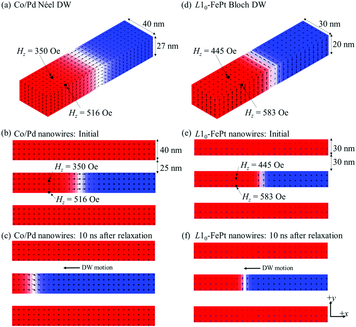 | ||
| Fig. 3 OOMMF simulations. In each case red and blue represent the component of magnetization out of the film plane and the arrows show magnetization vectors. (a) 3D schematic of a Co/Pd Néel DW and the magnitude of dipolar stray field experienced at the edge and center of the Co/Pd nanowire from its two nearest neighbors. (b) Plan-view of three Co/Pd nanowires, with a Néel DW in the center nanowire, and the outer nanowires magnetized ‘up’ (red). (c) Propagation of the ‘down’ domain (blue) by Néel DW motion to the left in the center Co/Pd nanowire driven by the stray field from its neighbors. (d) 3D schematic of a L10-FePt Bloch DW and the magnitude of dipolar stray field experienced at the edge and center of the L10-FePt nanowire from its two nearest neighbors. (e) Plan-view of three L10-FePt nanowires, with a Bloch DW in the center nanowire, and the outer nanowires magnetized ‘up’ (red). (f) Propagation of the ‘down’ domain (blue) by Bloch DW motion to the left in the center L10-FePt nanowire driven by the stray field from its neighbors. | ||
By comparing the energies of relaxed Néel and Bloch walls in a single Co/Pd nanowire, a Néel wall was taken as the equilibrium structure with a 6.4% lower energy [Fig. 3(a)]. When a domain wall was introduced into the center nanowire, the stray field from the neighboring nanowires produced DW motion leading to expansion of a domain with magnetization anti-parallel to that of the neighboring nanowires [Fig. 3(b and c)], indicating the stray fields will promote antiparallel wire magnetization at remanence.
The domains in a specific area of the Co/Pd nanowire array were imaged at remanence after AC demagnetization and after application of different reverse fields [Fig. 4(a)–(e)]. Fig. 5(a) shows the magnetic signal superimposed on the nanowire topography for the AFM and MFM data shown in Fig. 4(a). Many of the wires showed magnetization direction opposite to their neighbors as expected from the stray field. The fraction of wires showing magnetization antiparallel to that of their neighbors was calculated from MFM images by segmenting the 2 × 2 μm2 region in Fig. 5(a) into 100 portions of 0.2 × 0.2 μm2 each and summing the number of segments which contained a blue/red alternating magnetization configuration. It was determined that approximately 75% of neighboring Co/Pd nanowires displayed opposite contrast after AC demagnetization. This can be seen in Fig. 4(a) where the dark-light contrast in the MFM has double the period of the structure in the AFM, and the locations of DWs in neighboring wires are often adjacent to each other.
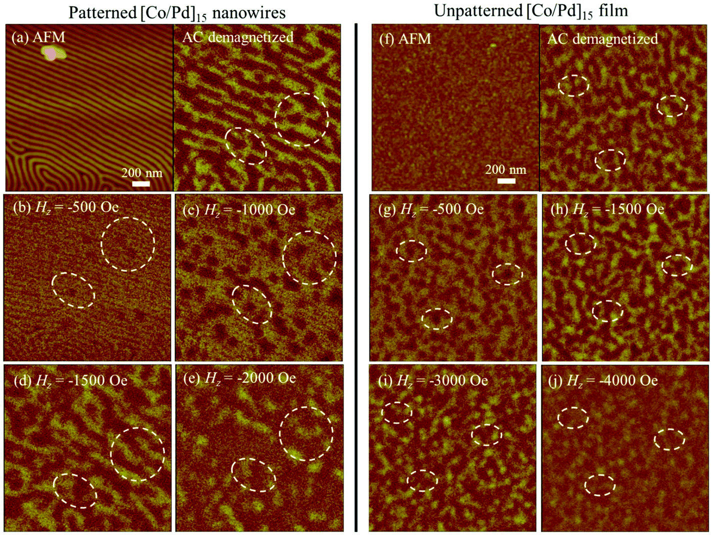 | ||
| Fig. 4 (a) AFM (left) and MFM (right) images of BCP patterned Co/Pd nanowires after AC demagnetization. (b–e) MFM images of Co/Pd nanowires at remanence after applying a field of Hz = (b) −500, (c) −1000, (d) −1500 and (e) −2000 Oe. (f) AFM (left) and MFM (right) images of unpatterned Co/Pd thin film after ac-demagnetization. (g–j) MFM images of unpatterned Co/Pd thin film at remanence after applying a field of Hz = (g) −500, (h) −1500, (i) −3000 and (j) −4000 Oe. All MFM images are captured at a fixed location on the patterned and unpatterned Co/Pd. Dashed circles indicate the same area on each image. Red and yellow contrast in the MFM images indicate ‘up’ and ‘down’ stray fields, respectively. | ||
 | ||
| Fig. 5 (a, b) 3D diagram showing the magnetic information (MFM) superimposed on the topography (AFM) of the ac-demagnetized (a) Co/Pd and (b) L10-FePt nanowires. Blue and red shading indicate ‘up’ and ‘down’ magnetization, respectively. (c, d) Area fraction of reversed domains versus applied reversed field as a percentage of saturation field for unpatterned and BCP patterned films of (c) Co/Pd and (d) L10-FePt. The dashed lines serve as a guide for the eye. The saturation field is taken to be the field at which the out-of-plane hysteresis loop closes. Saturation fields of the unpatterned Co/Pd, Co/Pd nanowires, unpatterned FePt film and FePt nanowires are 4.8, 3.2, 8.8, and 10.0 kOe, respectively. | ||
This result indicates a preferential antiparallel magnetization configuration of neighboring Co/Pd nanowires in the AC-demagnetized state as predicted from the micromagnetic simulation. Given the switching field distribution of Co/Pd nanowires (2440 Oe) and that the magnitude of the stray field just from the two closest neighbors (up to 516 Oe) is a large fraction of the Hc of the Co/Pd nanowires (790 Oe), the demagnetizing field is large enough to produce an antiparallel configuration in many of the wires. The correlated domain patterns parallel to the wires are in stark contrast to the domain arrangements in the unpatterned Co/Pd film [Fig. 4(f)]. The elongated domains in the Co/Pd nanowires had an average domain length of 460 ± 20 nm while the irregularly shaped domains in the unpatterned film had smaller average domain diameter of 270 ± 20 nm.
Even though most of the nanowires had antiparallel magnetization compared to their nearest neighbors, ∼25% of them displayed a parallel configuration. This is attributed to frustration when the nearest neighbors promote opposite magnetization of the center wire, giving degenerate ground states susceptible to small perturbations.44,45
To illustrate the reversal process of the array from saturation, the nanowires were first saturated with an out-of-plane field of Hz = 12 kOe giving a magnetization ‘down’ (yellow or light contrast) configuration. Different reverse fields were subsequently applied and the nanowire array was imaged at remanence. At a reverse field of Hz = −500 Oe [Fig. 4(b)], ‘up’ (red or dark contrast) domains with average size of 120 ± 20 nm nucleated in some of the nanowires. Specific reverse domains are identified (circled) so that changes in their geometry with increasing field can be seen. At an applied field of Hz = −1000 Oe [Fig. 4(c)], the existing ‘up’ domains, with average domain size of 190 ± 20 nm, expanded slightly but the clearest effect is an increase in the density of ‘up’ domains. These observations suggest limited domain wall mobility in the film such that domain nucleation occurs at lower fields than are required to translate the walls.
At Hz = −1500 Oe [Fig. 4(d)], the reverse domains expanded along the wires, reaching an average size of 540 ± 20 nm. Many regions of adjacent wires (e.g. circled on the right of the image) showed antiparallel magnetization between neighbors as was seen in the AC-demagnetized sample. The stray fields combined with the applied field encouraged expansion of the ‘up’ domains along the Co/Pd nanowires as predicted in the micromagnetic model to produce the antiparallel magnetization state. At applied fields above Hz = −2000 Oe [Fig. 4(e)], the ‘up’ domains further propagated leaving isolated ‘down’ domains stabilized by the stray fields.
A related behavior was seen in the unpatterned film where reverse domains formed at −500 Oe and further domains nucleated at −1500 Oe with little growth of the existing domains [Fig. 4(g and h)]. Larger fields led to expansion of the reverse domains [Fig. 4(i) and (j)] and at −4000 Oe only a few ‘down’ domains remained. The unpatterned and patterned films can be compared by plotting the fraction of reverse domains at remanence vs. field normalized to the saturation field, taken as 4.8 kOe for the unpatterned film and 3.2 kOe for the patterned film [Fig. 5(c)]. For the initial stages of reversal the patterned film had significantly more area fraction of reverse domains suggesting that domain nucleation was easier in the nanowires, presumably facilitated at the edges of the wires, but for larger fields the reverse domains expanded proportionately more in the unpatterned film as they were unconstrained by the wire edges.
We now describe the behavior of nanowire array made from a L10-FePt film. The BCP film on the L10-FePt thin film formed a less regular array of microdomains consisting of a mixture of cylinders, perforated lamellae [Fig. 1(b)] and partially interconnected double layer lamellae [Fig. 1(b) inset], compared to the BCP film on Co/Pd deposited and annealed under the same conditions. The BCP patterns on the L10-FePt had poor long-range ordering and larger rms line-edge roughness of 3.7 nm. The difference is believed to originate from variations in thickness of the BCP film on the rough L10-FePt thin film, which dramatically affects the BCP morphology.42 The L10-FePt thin film had a granular surface with high rms roughness of 2.9 (±0.5) nm (for comparison, the Co/Pd roughness was ∼0.8 ± 0.1 nm). In the regions of the L10-FePt film where nanowires had formed, their linewidth was 27 ± 8 nm, nanowire spacing was 30 ± 9 nm, center-to-center period was 63 ± 8 nm and measured rms edge roughness was 3.4 nm [Fig. 1(d)].
The unpatterned L10-FePt thin film had an out-of-plane easy axis with Hc,OP of 1.86 ± 0.05 kOe and an in-plane hysteresis loop with Hc,IP of 1.12 ± 0.05 kOe [Fig. 2(c)]. The XRD spectra of the unpatterned FePt thin film shows the FePt (001) superlattice peak and (002) fundamental peak (in ESI†), originating from ordering of the alternating Fe and Pt planes giving a (001)-textured fct L10-FePt. We attribute the (002) peak to the fct phase and not the fcc disordered phase because the (001) superlattice peak was present. The lack of a (200) fct peak indicates the film is textured with c-axis out of plane. Similar XRD results were shown in ref. 46 for an all-fct film. The extent of ordering is represented by the chemical ordering parameter,

Upon BCP pattern transfer onto the L10-FePt thin film, the magnetic moment per unit area decreased from 1.29 to 0.71 × 10⁻³ emu cm−2. This suggests that 55% of L10-FePt is left after patterning, which exceeds the estimated 46% areal coverage of cylindrical features calculated from the HIM image [Fig. 1(d)]. This can be explained by morphological variations in the BCP, in particular regions of double layer cylinders which led to unpatterned areas of the film.
Patterning led to a split of the (002) fundamental peak into two distinct peaks [Fig. 2(c) inset] which we attribute to fcc (200) and fct (002). We also see a reduction in the (001) intensity with respect to the net intensity around the (200) and (002) peaks: I001/(I002 + I200) = 0.30. These observations are interpreted as showing the formation of a disordered phase. Ref. 46 also shows two peaks for a mixed phase film. The fcc phase is assumed to form due to the redeposition of the Fe and Pt atoms during ion beam etching. It is unlikely for more fct phase to form during patterning because ordering temperatures are higher than the temperature during etching. Thus, we believe that the formation of additional disordered fcc FePt from the redeposition of FePt during pattern transfer, as well as possible strain relaxation, could have contributed to the reduction of the nanowire anisotropy Ku to 2.92 ± 0.26 × 10⁶ erg cm−3 [Fig. 2(d)]. The Hc,OP, Hc,IP and S* of the patterned nanowires also increased to 3.79 ± 0.05 kOe, 4.34 ± 0.05 kOe and 0.88 ± 0.18, respectively, presumably affected by the relatively large edge roughness, the inhomogeneity in the nanowire morphology and the crystal structure.
To examine the influence of dipolar stray field on the reversal process, OOMMF simulations were carried out on FePt nanowires with dimensions of 30 nm wide × 4000 nm long × 20 nm thick, a gap between adjacent nanowires of 30 nm, Ms of 644 emu cm−3, uniaxial out-of-plane Ku of 2.92 × 10⁶ erg cm−3, exchange constant of 1.3 × 10⁻⁶ erg cm−1 and damping constant of 0.1 [Fig. 3(d)–(f)]. Each nanowire consisted of 4 layers of cells with cell size of 5 nm × 5 nm × 5 nm. The effect of the tapered shape is neglected in the simulation because it is difficult to accurately capture the edge profile with a cell size of ∼5 nm. The total dipolar stray field experienced by the center L10-FePt nanowire along its midline and edge was 445 and 583 Oe, respectively [Fig. 3(d)]. Different from Co/Pd simulation results, both Néel and Bloch walls initiated in the L10-FePt nanowire relaxed to give a Bloch wall [Fig. 3(d)], which was taken as the energetically favourable DW structure for subsequent simulation [Fig. 3(e) and (f)]. In the absence of an external field and omission of pinning from defects and edge roughness, the stray field emitted from the ‘up’ neighbouring nanowires encouraged the expansion of the spin ‘down’ domain and propagation of the Bloch wall to the left [Fig. 3(f)].
Similar experimental protocols were used to examine the reversal of the L10-FePt nanowires as were used for the Co/Pd. A superimposed AFM-MFM image after AC-demagnetization [Fig. 5(b)] shows that an estimated 40% of the nearest-neighbor L10-FePt nanowires were antiparallel to their neighbors, less than observed for the Co/Pd sample. OOMMF calculations indicated that dipolar stray field (445–583 Oe) from the neighboring L10-FePt nanowires was much smaller than the coercivity Hc,OP (3.79 kOe) and hence the stray fields are less effective in determining the magnetization state. The AC-demagnetized L10-FePt nanowire sample had an average domain size of 425 ± 20 nm [Fig. 6(a)] which was similar to that of the uncorrelated labyrinth domain configurations in the unpatterned L10-FePt thin film with average domain size of 450 ± 20 nm [Fig. 6(f)].
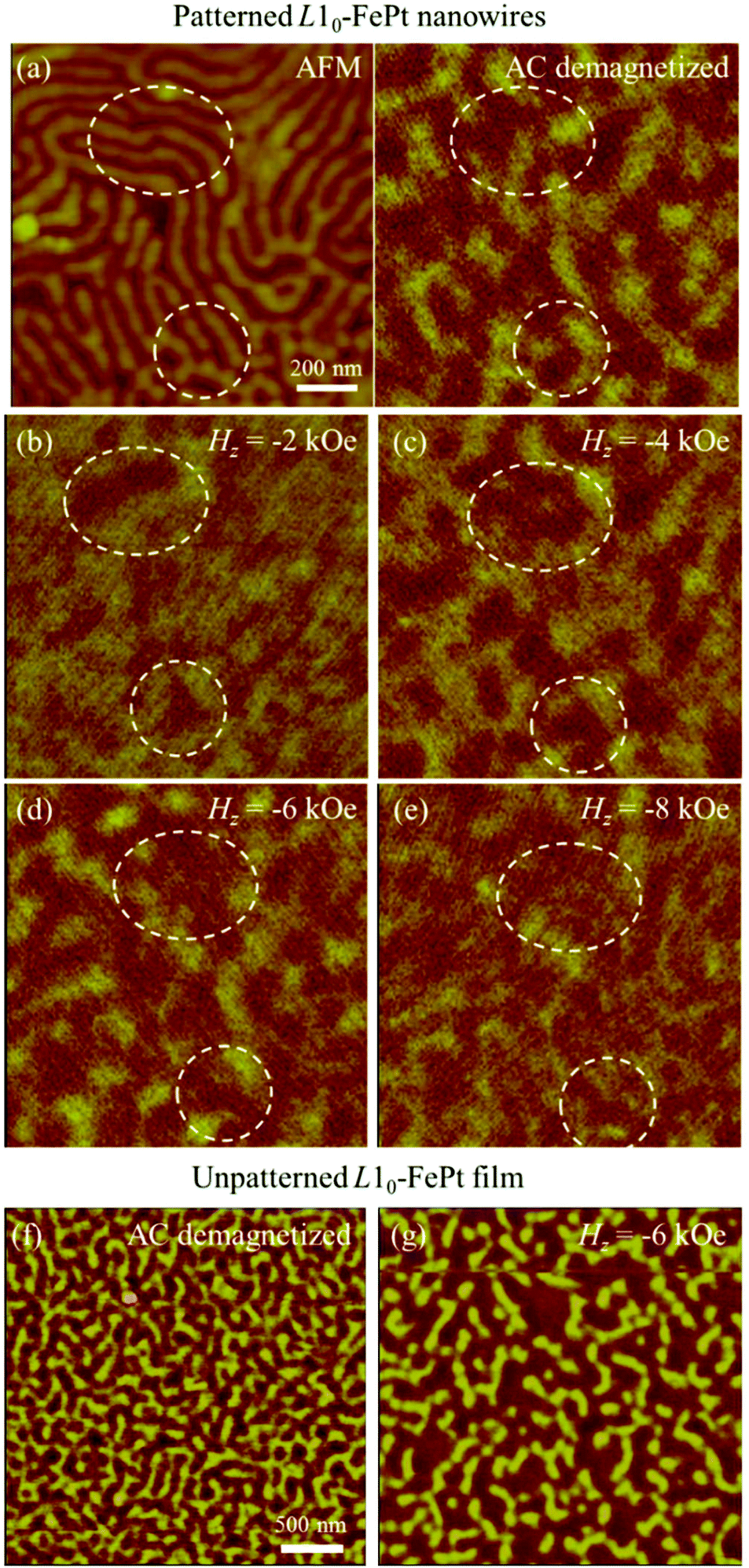 | ||
| Fig. 6 (a) AFM (left) and MFM (right) images of BCP patterned L10-FePt nanowires after ac-demagnetization. MFM images with applied field of Hz = (b) −2, (c) −4, (d) −6, (e) −8 kOe, captured at a fixed location on the sample. Dashed circles indicate the same area of sample on each image. MFM images of unpatterned L10-FePt after (f) ac-demagnetization and (g) applied field of Hz = −6 kOe. Red and yellow contrast in the MFM images indicate ‘up’ and ‘down’ magnetization, respectively. | ||
After saturation at Hz = 12 kOe, giving an initial ‘down’ configuration (yellow contrast), an applied field of Hz = −2 kOe [Fig. 6(b)] led to nucleation of reverse ‘up’ domains (red) which expanded at larger reverse fields [Fig. 6(c)–(e)]. There was no clear correlation of domains between adjacent wires, unlike in the Co/Pd sample. The reversal behaviour was similar to that of the unpatterned L10-FePt thin film [Fig. 6(g) and ESI†]. Furthermore, the area fraction of reverse domains vs. field was similar for the patterned and unpatterned L10-FePt film [Fig. 5(d)], suggesting that the reversal is dominated by intrinsic domain nucleation and growth rather than by the pattern geometry.
Conclusions
PMA [Co/Pd]15 and L10-FePt nanowire arrays with period 63 nm, linewidths of 27–38 nm, thickness of 20–27 nm and wire spacings of 26–30 nm were fabricated by ion beam etching using a carbon hard-mask patterned by a self-assembled PS-b-PDMS diblock copolymer mask, and the magnetic properties and reversal process were characterized. This process produced wires with a high aspect ratio (thickness/wire width = 0.71–0.74) with a predicted Néel domain wall structure in the Co/Pd and a Bloch wall in the FePt nanowires. In both cases dipolar stray fields from nearest neighbor wires are predicted to drive domain wall motion producing antiparallel magnetization directions in adjacent nanowires, but the ratio of stray field to coercivity is much higher for Co/Pd compared to FePt. Co/Pd nanowires showed a highly correlated domain structure in which adjacent wires had antiparallel magnetization and domain wall locations were aligned, as a result of the magnetostatic interactions. The study revealed domain nucleation was the dominant process at lower reverse fields with domain wall propagation occurring at higher reverse fields, i.e. the nanowires exhibit limited domain wall mobility. The L10-FePt nanowires were less regular due to the effect of the higher film roughness on the BCP morphology, and the stray field was much smaller than the coercivity. This led to only a limited correlation between the magnetization directions of nearest neighbor nanowires.Acknowledgements
The authors gratefully acknowledge the support of the Agency of Science, Technology and Research (A*STAR) International Fellowship grant, and C-SPIN, a STARnet Center of the Semiconductor Research Corporation sponsored by DARPA and MARCO. Shared experimental facilities of CMSE, an NSF MRSEC under award DMR1419807, were used.References
- J. Y. Cheng, A. M. Mayes and C. A. Ross, Nat. Mater., 2004, 3, 823–828 CrossRef CAS PubMed.
- C. T. Black, Nat. Nanotechnol., 2007, 2, 464–465 CrossRef CAS PubMed.
- C. A. Ross and J. Y. Cheng, MRS Bull., 2008, 33, 838–845 CrossRef CAS.
- B. D. Terris and T. Thomson, J. Phys. D: Appl. Phys., 2005, 38, R199–R222 CrossRef CAS.
- Y. S. Jung, J. H. Lee, J. Y. Lee and C. A. Ross, Nano Lett., 2010, 10, 3722–3726 CrossRef CAS PubMed.
- C. A. Ross, S. Haratani, F. J. Castaño, Y. Hao, M. Hwang, M. Shima, J. Y. Cheng, B. Vögeli, M. Farhoud, M. Walsh and H. I. Smith, J. Appl. Phys., 2002, 91, 6848 CrossRef CAS.
- K. H. Tu, W. Bai, G. Liontos, K. Ntetsikas, A. Avgeropoulos and C. A. Ross, Nanotechnology, 2015, 26, 375301 CrossRef PubMed.
- J. Y. Cheng, W. Jung and C. A. Ross, Phys. Rev. B: Condens. Matter, 2004, 70, 064417 CrossRef.
- Y. S. Jung and C. A. Ross, Small, 2009, 5, 1654–1659 CrossRef CAS PubMed.
- X. Yang, S. Xiao, W. Hu, J. Hwu, R. van de Veerdonk, K. Wago, K. Lee and D. Kuo, Nanotechnology, 2014, 25, 395301 CrossRef PubMed.
- Y. Kamata, A. Kikitsu, H. Hieda, M. Sakurai and K. Naito, J. Appl. Phys., 2004, 95, 6705–6707 CrossRef CAS.
- H. Hieda, Y. Yangita, A. Kikitsu, T. Maeda and K. Naito, J. Photopolym. Sci. Technol., 2006, 19, 425–430 CrossRef CAS.
- O. Hellwig, J. K. Bosworth, E. Dobisz, D. Kercher, T. Hauet, G. Zeltzer, J. D. Risner-Jamtgaard, D. Yaney and R. Ruiz, Appl. Phys. Lett., 2010, 96, 052511 CrossRef.
- F. Valdés-Bango, F. J. García Alonso, G. Rodríguez-Rodríguez, L. Morán Fernandez, A. Anillo, L. Ruiz-Valdepeñas, E. Navarro, J. L. Vicent, M. Vélez, J. I. Martín and J. M. Alameda, J. Appl. Phys., 2012, 112, 083914 CrossRef.
- J. Chai and J. M. Buriak, ACS Nano, 2008, 2, 489–501 CrossRef CAS PubMed.
- N. C. Bigall, B. Nandan, E. B. Gowd, A. Horechyy and A. Eychmüller, ACS Appl. Mater. Interfaces, 2015, 7, 12559–12569 CAS.
- T. R. Albrecht, H. Arora, V. Ayanoor-Vitikkate, J.-M. Beaujour, D. Bedau, D. Berman, A. L. Bogdanov, Y.-A. Chapuis, J. Cushen, E. E. Dobisz, G. Doerk, H. Gao, M. Grobis, B. Gurney, W. Hanson, O. Hellwig, T. Hirano, P.-O. Jubert, D. Kercher, J. Lille, Z. Liu, C. M. Mate, Y. Obukhov, K. C. Patel, K. Rubin, R. Ruiz, M. Schabes, L. Wan, D. Weller, T.-W. Wu and E. Yang, IEEE Trans. Magn., 2015, 51, 0800342 CrossRef.
- S. Bandyopadhyay and M. Cahay, Nanotechnology, 2009, 20, 412001 CrossRef PubMed.
- S. S. P. Parkin, M. Hayashi and L. Thomas, Science, 2008, 320, 190–194 CrossRef CAS PubMed.
- P. Ho, G. Han, K. He, G. M. Chow and J.-S. Chen, J. Appl. Phys., 2014, 115, 17C102 CrossRef.
- P. Ho, J. S. Zhang, D. C. Bono, J. S. Chen and C. A. Ross, Oersted field and spin current effects on magnetic domains in [Co/Pd]15 nanowires, IEEE Trans. Magn., 2016, DOI:10.1109/TMAG.2016.2526972.
- S. Ikeda, K. Miura, H. Yamamoto, K. Mizunuma, H. D. Gan, M. Endo, S. Kanai, J. Hayakawa, F. Matsukura and H. Ohno, Nat. Mater., 2010, 9, 721–724 CrossRef CAS PubMed.
- H.-R. Lee, K. Lee, J. Cho, Y.-H. Choi, C.-Y. You, M.-H. Jung, F. Bonell, Y. Shiota, S. Miwa and Y. Suzuki, Sci. Rep., 2014, 4, 6548 CrossRef CAS PubMed.
- C. Bi, Y. Liu, T. Newhouse-Illige, M. Xu, M. Rosales, J. W. Freeland, O. Mryasov, S. Zhang, S. G. E. te Velthuis and W. G. Wang, Phys. Rev. Lett., 2014, 113, 267202 CrossRef PubMed.
- J. Yuan, W. Pei, T. Hasagawa, T. Washiya, H. Saito, S. Ishio, H. Oshima and K. I. Itoh, J. Magn. Magn. Mater., 2008, 320, 736–741 CrossRef CAS.
- T. Wang, Y. Wang, Y. Fu, T. Hasegawa, F. S. Li, H. Saito and S. Ishio, Nanotechnology, 2009, 20, 105707 CrossRef CAS PubMed.
- Y. Endo, H. Fujimoto, S. Kumano, Y. Matsumura, I. Sasaki, Y. Kawamura, M. Yamamoto and R. Nakatani, J. Appl. Phys., 2008, 103, 07D918 CrossRef.
- M. R. Tabasum, F. Zighem, J. De La Torre Medina, A. Encinas, L. Piraux and B. Nysten, J. Appl. Phys., 2013, 113, 183908 CrossRef.
- C. Hassel, M. Brands, F. Y. Lo, A. D. Wieck and G. Dumpich, Phys. Rev. Lett., 2006, 97, 226805 CrossRef CAS PubMed.
- J. Kimling, T. Gerhardt, A. Kobs, A. Vogel, S. Wintz, M.-Y. Im, P. Fischer, H. P. Oepen, U. Merkt and G. Meier, J. Appl. Phys., 2013, 113, 163902 CrossRef.
- A. P. Mihai, F. Garcia-Sanchez, L. Vila, A. Marty, L. D. Buda-Prejbeanu, J. C. Pillet, C. Beigné, D. Ravelosona, C. Mannequin, J. C. Toussaint and J. P. Attané, Phys. Rev. B: Condens. Matter, 2011, 84, 014411 CrossRef.
- J. Zhang, P. Ho, J. A. Currivan-Incorvia, S. A. Siddiqui, M. A. Baldo and C. A. Ross, Appl. Phys. Lett., 2015, 107, 182408 CrossRef.
- D. Navas, C. Nam, D. Velazquez and C. A. Ross, Phys. Rev. B: Condens. Matter, 2010, 81, 224439 CrossRef.
- B. Y. Zong, P. Ho, G. C. Han, G. M. Chow and J. S. Chen, J. Micromech. Microeng., 2013, 23, 035038 CrossRef.
- E. C. Corredor, D. Coffey, M. Ciria, J. I. Arnaudas, J. Aisa and C. A. Ross, Phys. Rev. B: Condens. Matter, 2013, 88, 54418 CrossRef.
- S. Landis, B. Rodmacq and B. Diény, Microelectron. Eng., 2004, 73–74, 790–796 CrossRef CAS.
- G. Hu, T. Thomson, T. Rettner, S. Raoux and B. D. Terris, J. Appl. Phys., 2005, 97, 10J702 Search PubMed.
- S. Ishio, G. Q. Li, H. Takahoshi, H. Ito, H. Saito, T. Shima and K. Takanashi, J. Magn. Magn. Mater., 2004, 272–276, E819–E821 CrossRef CAS.
- J.-W. Liao, U. M. Atxitia, R. F. L. Evans, R. W. Chantrell and C.-H. Lai, Phys. Rev. B: Condens. Matter, 2014, 90, 174415 CrossRef.
- P. Ho, R. F. L. Evans, R. W. Chantrell, G. Han, G.-M. Chow and J. Chen, J. Appl. Phys., 2015, 117, 213901 CrossRef.
- V. Bellas, H. Iatrou and N. Hadjichristidis, Macromolecules, 2000, 33, 6993–6997 CrossRef CAS.
- M. J. Donahue and D. G. Porter, OOMMF User's Guide, Version 1.0, National Institute of Standards and Technology, Gaithersburg, MD, 1999 Search PubMed.
- W. Bai, A. F. Hannon, K. W. Gotrik, H. K. Choi, K. Aissou, G. Liontos, K. Ntetsikas, A. Alexander-Katz, A. Avgeropoulos and C. A. Ross, Macromolecules, 2014, 47, 6000–6008 CrossRef CAS.
- R. Moessner and A. P. Ramirez, Phys. Today, 2006, 59, 24–29 CrossRef CAS.
- S. Nakatsuji, Y. Nambu, H. Tonomura, O. Sakai, S. Jonas, C. Broholm, H. Tsunetsugu, Y. Qiu and Y. Maeno, Science, 2005, 309, 1697–1700 CrossRef CAS PubMed.
- M.-G. Kim and S.-C. Shin, J. Appl. Phys., 2001, 90, 2211–2215 CrossRef CAS.
Footnote |
| † Electronic supplementary information (ESI) available. See DOI: 10.1039/c5nr08865h |
| This journal is © The Royal Society of Chemistry 2016 |