
 Open Access Article
 This Open Access Article is licensed under a
 Creative Commons Attribution 3.0 Unported Licence
On the origin and magnitude of surface stresses due to metal nanofilms†
James
Bowen
 *a and
David
Cheneler
*b
*a and
David
Cheneler
*b
aDepartment of Engineering and Innovation, The Open University, Walton Hall, Milton Keynes, MK7 6AA, UK. E-mail: james.bowen@open.ac.uk
bDepartment of Engineering, Lancaster University, Bailrigg, Lancaster, LA1 4YR, UK. E-mail: d.cheneler@lancaster.ac.uk
First published on 28th January 2016
Abstract
Metallisation is a vital process for micro- and nanofabrication, allowing the controlled preparation of material surfaces with thin films of a variety of metals. The films are often subjected to further processing, including etching, patterning, chemical modification, and additional lamination. The extensive applications of metallised substrates include chemical sensors and nanoelectronics. Here, we report an experimental study of the metallisation of silicon cantilevers with nano-films of chromium and titanium. Analysis of the stress distribution throughout the cantilever showed that metallisation causes a constant stress along the length of the beam, which can be calculated from interferometric quantification of the beam curvature. The structure of the metal/silicon interface was imaged using electron microscopy in an attempt to ascertain the physical origin of the stress. A theoretical model is constructed for the stressed beam system, and it is shown that there is no single parameter that can describe the change in stress. The resultant structure after deposition varies significantly for each metal, which gives rise to a variety of stress directions and magnitudes.
Introduction
Many silicon based dynamic micro electromechanical systems (MEMS), for instance resonant pressure sensors, require metal deposition in order to be integrated with their control circuitry. These devices frequently comprise of compliant components such as beams or diaphragms. Deposition of metal on these structures affects their mechanical behaviour in a manner that is difficult to predict due to the presence of stresses induced in the system during deposition. Such stresses arise even when the conditions are controlled as to prevent thermal effects. Metallisation is an important intermediate step on the fabrication route to technologies including, but not limited to, microactuators,1 chemical detectors,2 resonators,3 and biosensors.4Controlling the shape and deflection of high aspect ratio microfabricated structures is of particular importance when considering the design and operation of sensing elements, such as microcantilevers of crystalline materials. Stoney reported the first consideration of stress in deposited films5 and since then studies have evolved to consider static deflections,6–13 dynamic properties,14–21 and thermal noise spectra22 in an effort to incorporate the influence of additional loading on mechanical properties. Additional informative works in this field include a model exploring the evolution of stress during surface oxidation processes23 and an investigation into the change in static deflection in response to an applied temperature change.24
The aim of this work was to study the effect of metallisation on the deflection of flexible Si beams; the variables explored were the metal deposited and the thickness of the metal film. Pre-metallised Si atomic force microscope (AFM) cantilevers were prepared using a focused ion beam (FIB) for transmission electron microscope (TEM) visualisation of the crystal structure at the metal/silicon interface. Cantilevers were metallised with Ti and Cr thin films. These metals are not only important in their own right, but are often used as adhesion promoters for Au films.25 Both metals can form strong bonds between the native silicon oxide and the Au film. Without an adhesive interlayer, Au thin films deposited directly on Si are notoriously fragile. Au surfaces are used for a range of technologies, in particular the deposition of self-assembled monolayers, which are a well-understood and customisable platform for the chemical modification of surfaces.26 Applications involving the deposition and adhesion of 2D nanomaterials such as graphene27 will also benefit from advancements in the understanding and control of thin film stresses. Previous theoretical investigations of surface stress imbalances at Si interfaces have shown promise for the construction of nanomechanochemical sensors28 and the formation of nanotubes,29 employing formulae based on Stoney5 for comparison. However, these studies have not resolved the origin of the surface stress; they have merely considered how the stresses could be exploited usefully. Further, the thickness of Si cantilevers which can be readily manufactured, and are commercially available, are typically much greater than those explored in these studies.
Classical laminated theory generally does not include the effects of interfacial or surface stress; here we report the development and application of a theory for laminated beams that takes into account the effect of this stress. By systematically depositing thin films of Ti and Cr onto one side of Si cantilevers it is shown that the magnitude and direction of this stress vary with the amount and type of metal deposited. We hypothesise that the stress is due to the lattice parameter mismatch between the metal thin film and the underlying Si. Further, the nature of the bonding between Si, native silicon oxide, and metal thin film will likely play an important role.
Experimental
Film deposition
Commercially available Si atomic force microscope (AFM) cantilevers (CSC12, MikroMasch, Estonia) were coated with thin films of either Cr (99.998% purity, Kurt J Lesker, USA) or Ti (99.995% purity, Kurt J Lesker, USA) using an Auto 500 electron beam evaporation system (Edwards, UK). Deposition rates were monitored in situ using a quartz crystal microbalance (QCM) and were in the range 10–100 pm s−1. Samples were held in place using 3M copper tape (RS Components, UK), and a water-cooled target was used to prevent thermal expansion effects.Atomic force microscopy (AFM)
The thickness and spring constants of the unmodified cantilevers were obtained according to the method previously described by Bowen et al.30 The frequency of the first resonant mode of each cantilever was measured at 18 °C and 40% relative humidity, using a NanoWizard II AFM (JPK Instruments, UK).Film thickness
The thickness of the native oxide SiOx/SiO2 layer on the Si cantilevers was performed using a UVISEL spectroscopic ellipsometer (Horiba Scientific, UK) operating a Xe light source. The angle of incidence was fixed at 70°, and a wavelength range of 250–800 nm was used. DeltaPsi software was employed to determine the thickness values and the calculations were based on a three-phase ambient/SiO2/Si(100) model, in which the SiO2 was assumed to be isotropic.Beam deflection
Analysis of cantilever shape was performed using a MicroXAM2 white light interferometer (Omniscan, UK) operating a 10× lens (Nikon, UK). Acquired data was processed using SPIP software (Image Metrology, Denmark). Following export as ASCII, data were further analysed using Matlab (MathWorks, UK).X-ray photoelectron spectroscopy (XPS)
XPS analysis of films was performed using a custom-built instrument operating an Al Kα X-ray source, providing a monochromatic X-ray beam with incident energy of 1486.68 eV and a circular spot of ∼4 mm2 area. The region of the cantilever chip adjacent to the fixed end of the cantilever beam was analysed. The measurements were made at a pressure of ∼1 × 10⁻⁸ mbar, and samples were immobilized onto stainless steel sample holders using double-sided Shintron carbon sticky tape (Agar Scientific, UK). Low resolution survey spectra were obtained using a pass energy of 150 eV over a binding energy range of −10 to 1200 eV with 1 eV increments. High resolution spectra were obtained using a pass energy of 20 eV over a binding energy range of 20–30 eV, centred around a chosen photoelectron binding energy with 0.1 eV increments. A dwell time of 0.5 s was employed when collecting data from each binding energy increment for all measurements.Transmission electron microscopy (TEM)
Cantilever cross-sections were prepared using an Auriga focused ion beam scanning electron microscope (FIB-SEM, Zeiss, Germany). A sacrificial platinum layer was deposited atop the metallised surface of the cantilever, to protect it from the milling beam. The crystal structure of the modified cantilever at the interface between the Si and metal film was then analysed using a Titan 80-30 TEM (FEI, USA). The chemical composition of the metal layer was analysed using energy-dispersive X-ray spectroscopy (EDX) and electron energy loss spectroscopy (EELS).Results and discussion
Beam shape due to metallisation
The beam shape post-metallisation exhibits significant curvature in either the tensile or compressive direction (Fig. 1). The convention we employ here is that (i) tensile surface stresses curve the coated side of the beam downwards, whilst (ii) compressive surface stresses curve the coated side of the beam upwards. The beam in the top image is coated with 12 nm Ti, causing a tensile surface stress. The beam in the lower image is coated with 12 nm Cr, causing a compressive surface stress.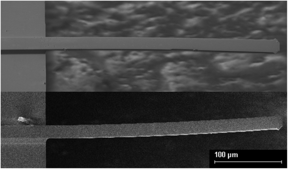 | ||
| Fig. 1 SEM images of cantilevers metallised on their upper surface only: top image shows a 350 μm beam coated with a 12 nm Ti film, causing a tensile stress; bottom image shows a 350 μm beam coated with a 12 nm Cr film, causing a compressive stress. | ||
Quantification of the curvature was performed using interferometric analysis (Fig. 2). Beams coated with 12 nm Cr (Group 1) exhibit a more pronounced curvature due to compressive surface stress than beams coated with 6 nm Cr (Group 2). Uncoated beams exhibit no curvature (Group 3). Beams coated with 4.5 nm Ti (Group 4) exhibit curvature due to tensile surface stress, the curvature being more pronounced for beams coated with 12 nm Ti (Group 5). The surface stresses generated by the Ti and Cr films are such that a beam of approximate dimensions 100 × 35 × 1 μm (length, width, thickness) is curved upwards or downwards by 1 μm due to the presence of a 12 nm metal film. The radius of curvature of these beams is on the order 10 mm. Classical analysis of cantilever beam deflection under its own weight suggests that unmodified cantilevers would exhibit maximum downward deflections of the order 95 pm. The presence of a Cr or Ti film of 12 nm thickness might be expected to add 3–5 nm of downwards deflection. The metal film masses are in the range 1–4% of the beam mass. These calculations are provided in the ESI.† It is certainly not possible to rationalise an upwards deflection using classical analysis.
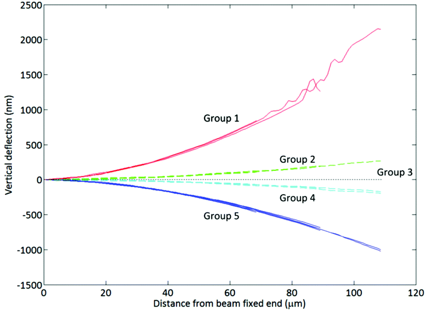 | ||
| Fig. 2 Interferometric analysis of 90–130 μm length cantilevers with and without metallisation. There are five groups of data presented. Group 1 (top) are cantilevers with a 12 nm Cr film. Group 2 cantilevers with a 6 nm Cr film. Group 3 are uncoated cantilevers. Group 4 are cantilevers with a 4.5 nm Ti layer. Group 5 (bottom) are cantilevers with a 12 nm Ti layer. | ||
Interface structure
Examination of the structure of the interface between the beam surface and metal film was performed using transmission electron microscopy (TEM). For the Ti interface (Fig. 3) the crystalline Si can be clearly seen, with an amorphous 3 nm thickness native oxide (SiOx/SiO2) layer immediately adjacent to the 12 nm Ti film, which exhibits a polycrystalline structure.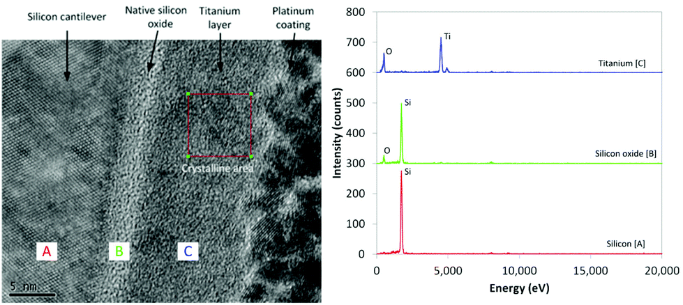 | ||
| Fig. 3 TEM cross-section of interface structure for Ti coated beam, with EDX spectra for the silicon, silicon oxide, and titanium regions. | ||
Particles of crystalline Ti with diameters ca. 5 nm can be observed throughout the layer; this was confirmed by fast Fourier transform (FFT) analysis of the X-ray scattering exhibiting a cell size of approximately 295 pm, commensurate with the reported 290 pm diameter of Ti atoms in crystalline metal.29 The amorphous structures can form due to the oxidation of Ti with the small amounts of O2 remaining in the partial vacuum during deposition; the presence of O is confirmed by energy-dispersive X-ray (EDX) analysis (Fig. 3). X-ray photoelectron spectroscopy (XPS) analysis (Fig. 4) further confirms the presence of Ti and O in the 4.5 nm and 12 nm films.
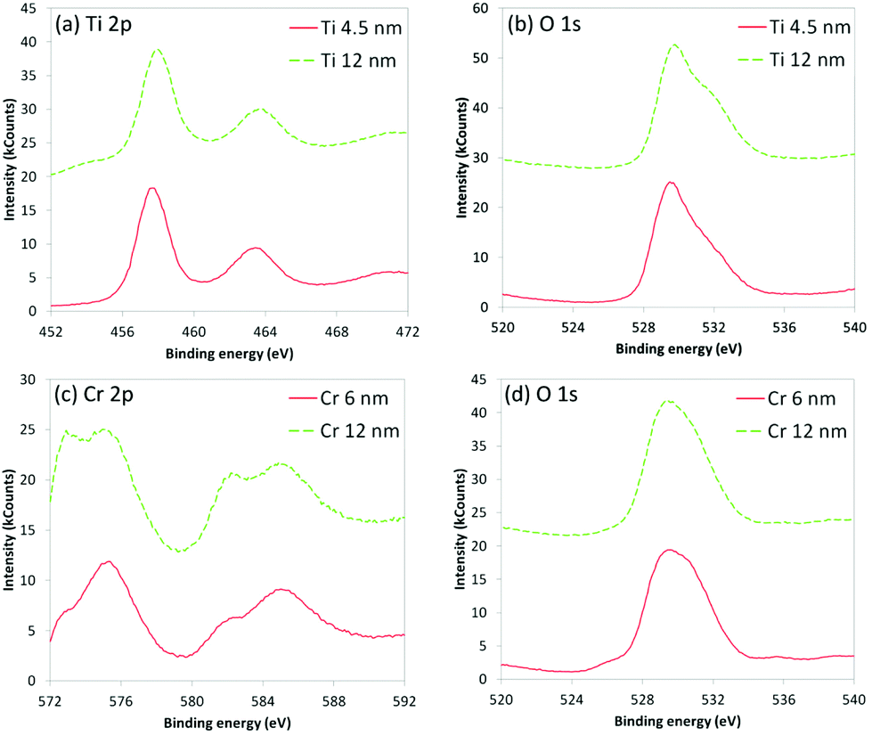 | ||
| Fig. 4 XPS spectra for Si beams coated with Ti and Cr films: (a) Ti 2p3/2 and Ti 2p1/2 for Ti film, (b) O 1s for Ti film, (c) Cr 2p3/2 and Cr 2p1/2 for Cr film, (d) O 1s for Cr film. | ||
For the Cr interface (Fig. 5) the crystalline Si can be seen, with an amorphous 3 nm thickness native oxide (SiOx/SiO2) layer immediately adjacent to the 12 nm Cr film, in which crystalline regions are visible. FFT confirmed that this layer was metallic Cr. Unlike the Ti film however, the Cr layer terminates with a CrOx layer, which may form upon exposure of the freshly deposited Cr to atmospheric oxygen. The presence of O in this amorphous layer is confirmed by EDX analysis (Fig. 5), whilst XPS analysis (Fig. 4) further confirms the presence of Cr and O in the 6 nm and 12 nm films. The XPS results also indicate that there are two distinct binding environments; 2p3/2 photoelectrons from metallic Cr exhibiting a binding energy of 573 eV, whilst 2p3/2 photoelectrons from CrOx exhibiting a binding energy of 575 eV.
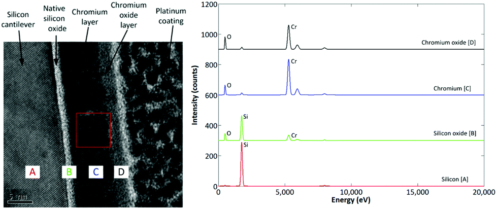 | ||
| Fig. 5 TEM cross-section of interface structure for Cr coated beam, with EDX spectra for the silicon, silicon oxide, chromium, and chromium oxide regions. | ||
Surface stresses
The stress distribution at the silicon/metal interface was calculated by fitting eqn (1) to the vertical curvature of the cantilevers, as measured using white light interferometry (Fig. 6). A two-dimensional beam theory that captures the stress distribution due to a constant shear stress at the surface was developed, in which the axial and vertical displacements of the beam are considered. The full derivation is presented in the ESI.†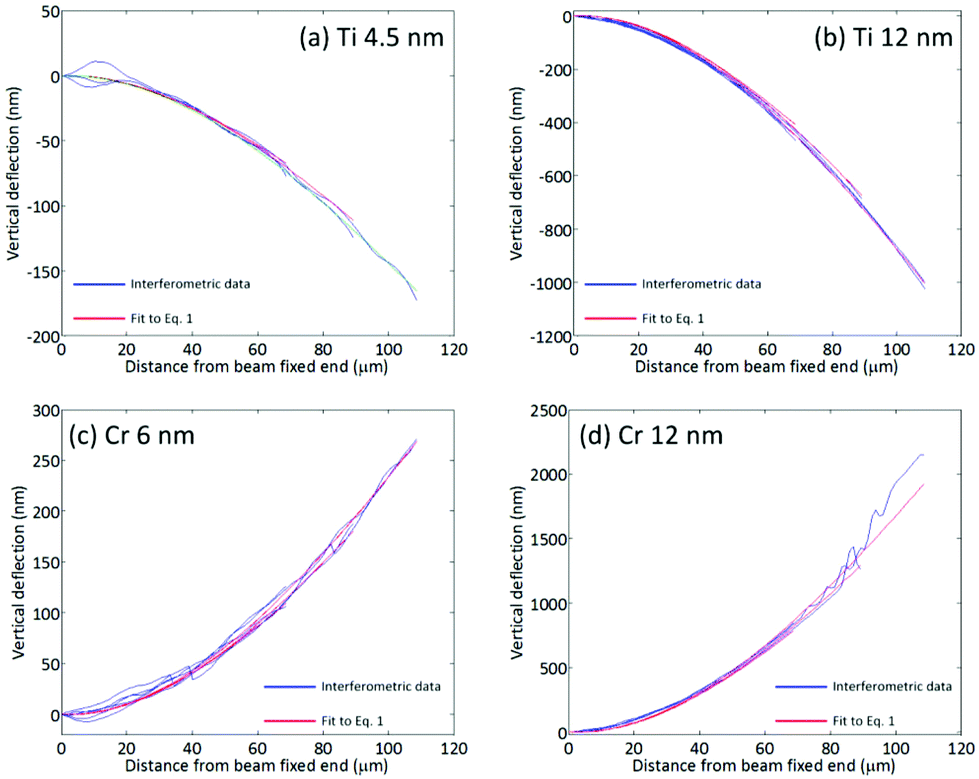 | ||
| Fig. 6 Measured beam curvature and fit to eqn (1) for (a) 4.5 nm Ti film, (b) 12 nm Ti film, (c) 6 nm Cr film, and (d) 12 nm Cr film. | ||
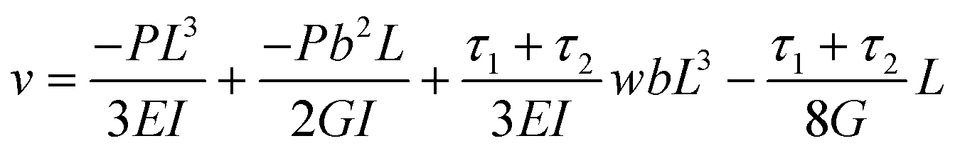
The vertical displacement of the beam, ν, is described by:
 | (1) |
The shear stress due to metallisation of the upper surface (ESI, Table 1†) is a function of both the beam length and the thickness of the deposited metal film. Cr films and Ti films cause surface stresses which act in opposite directions to each other. Further, for a given film thickness, Cr films cause a surface shear stress of greater magnitude than Ti films. The specific surface stress, β, for each beam length and metal film thickness, tmetal, can be calculated using eqn (2).
 | (2) |
The values of β for Ti films are −0.25 nN nm−2 (4.5 nm) and −0.56 nN nm−2 (12 nm), whereas for Cr films the values of β are 0.30 nN nm−2 (6 nm) and 1.08 nN nm−2 (12 nm). The relationship between film thickness and surface shear stress is indicative of an as-yet unresolved complex interaction between the metal film and the Si beam. There is an approximate correlation between the magnitude of the shear modulus for the metal film, and the magnitude of the beam deflection. Cr exhibits a shear modulus of 115 GPa, whereas Ti exhibits a shear modulus of 40 GPa. Future work on this topic should seek to explore the possible importance of this parameter.
The geometric arrangement of atoms at and around the beam/film interface should also be considered, particularly the possibility of competition for O atoms from the native silicon oxide layer upon deposition of the metal atoms. Consideration of the atomic diameters and the stoichiometry of the likely metal oxides which could form at the interface suggests that TiO2 formation could lead to a compressive stress, causing a downwards beam curvature. This is because TiO2 and SiO2 exhibit the same stoichiometry, yet Ti atoms exhibit a larger diameter (290 pm) than Si atoms (232 pm).31 Interestingly, with Cr atoms having diameters (250 pm) much closer to Si atoms, and with Cr2O3 exhibiting a stoichiometry with a different metal/oxygen ratio to SiO2 and TiO2, the origins of the compressive stress and upwards beam curvature may be partly attributable to space filling effects.
An alternative approach is to consider the dimensions of the unit cells of each material, full details of which can be found in the ESI.† This analysis characterises the strain, ε, due to lattice mismatch between the metal film and the substrate.32 It is shown that both Ti and Cr films should both be in tension, i.e. upwards beam deflection. However, this is clearly not the case for the results obtained in this work, with opposing directions of beam deflection measured for Cr and Ti. It is likely that the structure of the deposited films prevents accurate analysis of crystal orientation effects, such as those performed by Shilo et al.,33 who used X-ray diffraction to examine strains in LiNbO3. Hence, a predictive approach based on unit cell dimensions seems to be inappropriate here.
Implications for micro/nanomanufacture
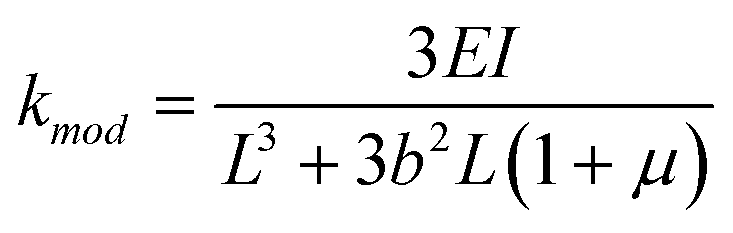
The induced deformation caused by the metallisation can impact compliant micro and nano devices in a number of ways, both beneficial and deleterious. The most obvious repercussion would be a change of stiffness in the cantilever. Standard theory derived from the strength of materials gives the nominal stiffness of a rectangular cantilever as:28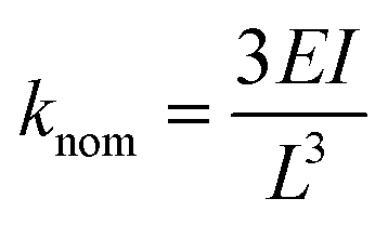 | (3) |
However, from eqn (38) in the ESI† the peak deflection of the cantilever due to a point force acting downwards on the tip can be shown to be:
 | (4) |
Letting the algebraic sum of the stresses equal τ0, and using the standard definition of the shear stress,
 | (5) |
 | (6) |
The first term in the denominator is the same as given in eqn (3). The second term is due to the shear stresses in the cantilever induced by just the point load and has appeared owing to the higher order derivation used here. Frequently, it is thin cantilevers that are of interest. In this case, the stiffness reduces to the nominal stiffness given by eqn (3). Therefore the surface stress does not affect the stiffness. It does however cause a finite tip deflection, given by eqn (4), even when the point force is zero.
Following Bowen et al.,30 the resonant frequency of the beam becomes:
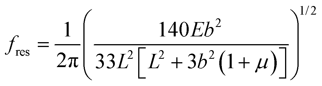 | (7) |
Again this is not affected by the surface stress and reduces to the classical expression when the beam is very thin. This result was previously observed by Bowen et al.30 for coated Si cantilevers with resonant frequencies in the range 80–220 kHz.
When the surface stress is positive, i.e. compressive, the beam is curved upwards so that an applied point force acts to straighten the beam. The beam only becomes flat when
| P = τ0wb | (8) |
If the amplitude of oscillations are small, it is possible that the surface stresses preserve the direction of the normal stresses within the beam while it oscillates, i.e. a surface in tension may remain in tension, whereas in an unstressed beam the stress will fluctuate between compression and tension. The stresses in this case will also be larger in magnitude (see eqn (14) in section 2 of the ESI†). This will have an impact on the fatigue life of the beam. Traditionally, it was believed that Si was immune to fatigue, however, it was observed recently that micro-scale Si structures may succumb to fatigue failure34 limiting the useful life of the structure. Normally, fatigue occurs when a structure is exposed to repeated cycles of varying stress. Cracks can form and propagate when a structure is under tension. In Si, this can expose fresh Si which then oxidizes resulting in further stress and crack propagation.34 This is more likely to be the case if crack initiation sites exist due to prior fabrication processes, such as dry etch and release processes which result in a rough surface finish.35
Metallisation of a Si structure can affect the fatigue life in two ways. If the metallised surface results in a tensile surface stress, the opposite surface may remain in compression throughout the entire oscillation cycle preventing cracks from being opened and exposing fresh Si. The metallised surface itself may also hinder further oxidation of the surface in tension. In this way, one would expect the metallisation process to improve the nominal fatigue life of the component. However, the inverse is also true. If the metallised surface results in a compressive stress, the opposite surface may remain in tension and unprotected. In this state, cracks are more likely to open and become oxidized, thus reducing the fatigue life of the component.
Having a curved surface can be advantageous in the field of optoelectronics,36,37 in particular in the design of optical systems for digital cameras.38 Metallisation may be a convenient way of controlling the curvature of light focusing arrays, with the added advantage that external forces can be used to modify the curvature further, perhaps to remove aberrations such as astigmatism. The curvature of the beam, κ, is defined by:
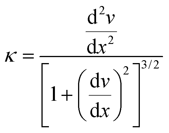 | (9) |
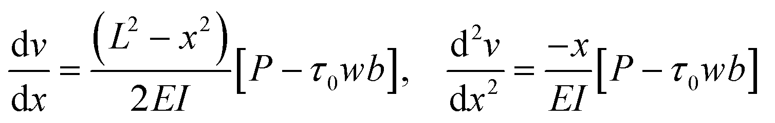 | (10) |
This means the curvature of the beam varies along its length. This is in contradiction with the classic model by Stoney5 who assumed perfect bending and hence derived a constant curvature along the beam. As can be seen in Fig. 7, the trend is essentially linear and varies from 0 m−1 at x = 0 to the peak curvature, −L[P − τ0wb]/EI, at x = L. Therefore, a system which can focus on different parts of the beam can take advantage of the change in the local curvature.
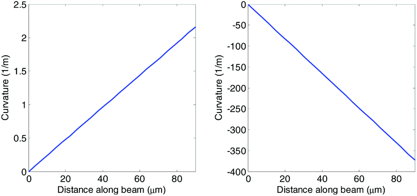 | ||
| Fig. 7 Curvature of beam as a function of position along beam. Beam Cr 10 used as an example (see Table S1† for dimensions). Left: point force taken to be zero – note positive surface stress and positive curvature. Right: point force taken as 3.75 μN which is the force required to deflect the unmetallised cantilever by 1 μm. | ||
Suggestions for future research
The methodology described here presents a valuable tool for studying surface shear stresses for a wide range of materials. Significant further work is required to determine the nature of this interaction, exploring a diverse range of metals such as Ag, Al, Ga, Ge, Ni, Pd, Pt, Sn, Ta, Zn, and Zr. It is also known that films including Au and Cu adhere poorly to Si, necessitating the use of an adhesion-promoting interlayer. Ascertaining whether surface shear stresses are produced due to metals which do not adhere well to Si will be of great value also. Extending the analysis to non-metals could also be of benefit, particularly materials which readily oxidise upon exposure to O2. For example, Au does not form a native oxide, and the possibility of competition for O atoms at the beam/metal interface could be explored through the deposition of Au films.The question of when the stress arises is intriguing; the possibility of constructing a custom apparatus to performing in situ monitoring of beam curvature during film deposition is highly desirable. Such a study would provide insight into the mechanisms and interactions which give rise to the curvature. In situ monitoring of film growth would also be of benefit, perhaps affording insights regarding the growth model for the film. Acquisition of surface topographical data has previously been used to predict the growth model and intrinsic stresses within metal films.39 Such analysis would require the construction of a bespoke apparatus, with a scanning tunnelling microscopy analysis area available under vacuum. Further, the ability to acquire spectroscopic information using an ellipsometer would permit information regarding the thin film structure to be obtained and modelled.40 Monitoring the structure and topography of the film in situ during deposition and growth is an intriguing method, from which data the origin of these surface stresses could be interpreted.
Previous research has examined the structure of the Ti film deposited on SiO2 surfaces. Iida and Abe41 employed XPS and X-ray diffraction (XRD), reporting that the nature of the bonding between SiO2 and Ti depends on the crystal structure of the SiO2 surface, and that bonding occurs even at room temperature. Butz and Wagner42 employed electron energy loss spectroscopy (EELS) to investigate the interaction of 1–2 layers of Ti atoms with the SiO2 surface. The conclusion of this work was that Ti reduces SiO2 through the formation of Ti–O bonds, and changes the Si–O–Si bond angle for the surface layer of atoms. Undertaking EELS measurements during deposition would provide important insight regarding the initial stages of bonding and competition for O atoms.
Additionally, the ability to vary the beam temperature during film deposition, and post-deposition, would allow the investigation of energy minimisation and annealing effects. I.e. Does the addition of thermal energy permit the metal film to reorganise, reducing the magnitude of the surface stress/beam curvature, and possibly the film thickness dependence? This does however increase the possibility of metal atom diffusion into the SiO2 layer.43 Further work should also include the use of plates as well as beams, non-Si substrates, and anisotropic surfaces, for example lithographically patterned materials. It would be of great benefit to perform further experimental investigations alongside computational efforts, simulating the deposition and arrangement of atoms on the substrate. The direction and magnitude of any strains induced due to film growth could hence be calculated.
Conclusions
We report that silicon microcantilevers coated with certain metals undergo a static deflection along their major axis, the direction of curvature depending upon the nature of the metal/silicon interaction. Cantilevers with a range of lengths have been coated with chromium and titanium with different thicknesses have been analysed using TEM, EDX and EELS in order to ascertain the physical origin of this stress. It was shown that there is no single parameter that can describe the change in stress as a function of the metal or film thickness. This is because the resultant structure after deposition varies significantly for each metal. Analysis of the stress distribution throughout the cantilever showed that metallisation causes a constant stress along the length of the beam, which can be calculated using interferometric data.The methodology presented here provides a valuable tool for studying this phenomenon in greater detail for a wide range of metals. Extending the methodology further to non-metals could also be of benefit, particularly when considering those materials which readily oxidise upon exposure to O2. Understanding the magnitude and direction of surface stresses for nanofilms deposited on flexible substrates will be of benefit to academia and industry, not least those concerned with the design and manufacture of MEMS devices and optoelectronics.
Acknowledgements
This work was in part funded by the Researchers Exchange Program as part of the EUMINAfab project (grant agreement no. FP7-226460). The MicroXAM2 Interferometer and JPK Instruments NanoWizard II Atomic Force Microscope used in this research were obtained, through Birmingham Science City: Innovative Uses for Advanced Materials in the Modern World (West Midlands Centre for Advanced Materials Project 2), with support from Advantage West Midlands (AWM) and part funded by the European Regional Development Fund (ERDF). The authors thank Dr Dominic Walliman for his assistance with the electron beam evaporation process. The authors also thank the staff at the CRANN facility at Trinity College Dublin for access to, and support in using, the Zeiss Auriga FIB and FEI Titan TEM.References
- W.-H. Chu, M. Mehregany and R. L. Mullen, J. Micromech. Microeng., 1993, 3, 4 CrossRef CAS.
- H.-J. Butt, J. Colloid Interface Sci., 1996, 180, 251 CrossRef CAS.
- R. Narkowicz, D. Suter and R. Stonies, J. Magn. Reson., 2005, 175, 275 CrossRef CAS PubMed.
- Y. Nagai, J. D. Carbajal, J. H. White, R. Sladek, P. Grutter and R. B. Lennox, Langmuir, 2013, 29, 9951 CrossRef CAS PubMed.
- G. G. Stoney, Proc. R. Soc. London, Ser. A, 1909, 82, 172 CrossRef CAS.
- J. E. Sader, J. Appl. Phys., 2001, 89, 2911 CrossRef CAS.
- M. T.-K. Hou and R. Chen, J. Micromech. Microeng., 2003, 13, 141 CrossRef.
- Y. Zhang, Q. Ren and Y.-P. Zhao, J. Phys. D: Appl. Phys., 2004, 37, 2140 CrossRef CAS.
- M. J. Lachut and J. E. Sader, Phys. Rev. Lett., 2007, 99, 206102 CrossRef PubMed.
- M. J. Lachut and J. E. Sader, Appl. Phys. Lett., 2009, 95, 193505 CrossRef.
- M. Godin, V. Tabard-Cossa, Y. Miyahara, T. Monga, P. J. Williams, Y. Beaulieu, B. R. Lennox and P. Grutter, Nanotechnology, 2010, 21, 075501 CrossRef PubMed.
- M. X. Shi, B. Liu, Z. Q. Zhang, Y. W. Zhang and H. J. Gao, Proc. R. Soc. London, Ser. A, 2012, 468, 2595 CrossRef.
- L. Aprilia, R. Nuryadi and D. Hartanto, Int. J. Comput. Eng. Res., 2013, 3, 53 Search PubMed.
- J. Lagowski and H. C. Gatos, Surf. Sci., 1974, 45, 353 CrossRef CAS.
- J. Lagowski, H. C. Gatos and E. S. Sproles Jr., Appl. Phys. Lett., 1975, 26, 493 CrossRef CAS.
- M. E. Gurtin, X. Markenscoff and R. N. Thurston, Appl. Phys. Lett., 1976, 29, 529 CrossRef CAS.
- Q. Ren and Y.-P. Zhao, Microsyst. Technol., 2004, 10, 307 CrossRef CAS.
- A. W. McFarland, M. A. Poggi, M. J. Doyle, L. A. Bottomley and J. S. Colton, Appl. Phys. Lett., 2005, 87, 053505 CrossRef.
- V. Pini, J. Tamayo, E. Gil-Santos, D. Ramos, P. Kosaka, H.-D. Tong, C. van Rijn and M. Calleja, ACS Nano, 2011, 5, 4269 CrossRef CAS PubMed.
- F. Yang, Langmuir, 2012, 28, 3449 CrossRef CAS PubMed.
- L. Sirghi, D. Ciumac and V. Tiron, Thin Solid Films, 2014, 565, 267 CrossRef CAS.
- J. Laurent, A. Steinberger and L. Bellon, arXiv, 2013, arXiv:1302.2583v2 [cond-mat.mes-hall].
- Y. Suo and S. Shen, J. Appl. Phys., 2013, 114, 164905 CrossRef.
- D. Ramos, J. Mertens, M. Calleja and J. Tamayo, Sensors, 2007, 7, 1757 CrossRef.
- C. A. Goss, D. H. Charych and M. Majda, Anal. Chem., 1991, 63, 85 CrossRef CAS.
- A. Ulman, Chem. Rev., 1996, 96, 1533 CrossRef CAS PubMed.
- K. J. Koski and Y. Cui, ACS Nano, 2013, 7, 3739 CrossRef CAS PubMed.
- J. Zang and F. Liu, Nanotechnology, 2007, 18, 405501 CrossRef.
- J. Zang, M. Huang and F. Liu, Phys. Rev. Lett., 2007, 98, 146102 CrossRef PubMed.
- J. Bowen, D. Cheneler, D. Walliman, S. G. Arkless, Z. Zhang, M. C. L. Ward and M. J. Adams, Meas. Sci. Technol., 2010, 21, 115106 CrossRef.
- G. H. Aylward and J. V. Tristan, SI Chemical Data, Wiley, New York, 6th edn, 2008 Search PubMed.
- W. K. Liu and M. B. Santos, Thin Films: Heteroepitaxial Systems, World Scientific, Singapore, 1999, vol. 15 Search PubMed.
- D. Shilo, E. Lakin and E. Zolotoyabko, Phys. Rev. B: Condens. Matter, 2001, 63, 205420 CrossRef.
- D. H. Alsem, O. N. Pierron, E. A. Stach, C. L. Muhlstein and R. O. Ritchie, Adv. Eng. Mater., 2007, 9, 15 CrossRef CAS.
- L. Haobing and F. Chollet, J. Microelectromech. Syst., 2006, 15, 541 CrossRef.
- T.-K. A. Chou and K. Najafi, Micro Electro Mech. Sys., The 15th IEEE Int. Conf. on. IEEE, 2002, p. 145 Search PubMed.
- J. Kim, Y. H. Kim, S. H. Choi and W. Lee, ACS Nano, 2011, 5, 5242 CrossRef CAS PubMed.
- S. B. Rim, P. B. Catrysse, R. Dinyari, K. Huang and P. Peumans, Opt. Express, 2008, 16, 4965 CrossRef PubMed.
- S. G. Mayr and K. Samwer, Phys. Rev. Lett., 2001, 87, 036105 CrossRef CAS PubMed.
- D. E. Aspnes, Thin Solid Films, 1982, 89, 249 CrossRef CAS.
- S. Iida and S. Abe, Appl. Surf. Sci., 1994, 78, 141 CrossRef CAS.
- R. Butz and H. Wagner, Phys. Status Solidi A, 1986, 94, 71 CrossRef CAS.
- J. D. McBrayer, R. M. Swanson and T. W. Sigmon, J. Electrochem. Soc., 1986, 133, 242 CrossRef.
Footnote |
| † Electronic supplementary information (ESI) available: 1. Cantilever preparation for transmission electron microscopy analysis of the interface structure. 2. Theoretical consideration of beam vertical deflection under the action of surface shear stresses. 3. Calculated surface shear stresses due to beam metallisation. 4. Calculated beam deflections due to uniformly distributed loads. 5. Strain due to heteroepitaxial film growth. See DOI: 10.1039/c5nr08789a |
| This journal is © The Royal Society of Chemistry 2016 |