
 Open Access Article
 This Open Access Article is licensed under a Creative Commons Attribution-Non Commercial 3.0 Unported Licence
Identification of the current path for a conductive molecular wire on a tripodal platform†
M. A.
Karimi
a,
S. G.
Bahoosh
a,
M.
Valášek
b,
M.
Bürkle
c,
M.
Mayor
bde,
F.
Pauly
a and
E.
Scheer
*a
aDepartment of Physics, University of Konstanz, 78457 Konstanz, Germany. E-mail: Elke.scheer@uni-konstanz.de
bKarlsruhe Institute of Technology (KIT), Institute of Nanotechnology, P.O. Box 3640, 76021 Karlsruhe, Germany
cNanosystem Research Institute (NRI) ‘RICS’, National Institute of Advanced Industrial Science and Technology (AIST), Tsukuba, Ibaraki 305-8568, Japan
dDepartment of Chemistry, University of Basel, 4056 Basel, Switzerland
eLehn Institute of Functional Materials (LIFM), Sun Yat-Sen University (SYSU), Xingang Rd. W., Guangzhou, China
First published on 3rd May 2016
Abstract
We present the chemical synthesis as well as charge transport measurements and calculations for a new tripodal platform based on a rigid 9,9′-spirobifluorene equipped with a phenylene-ethynylene wire. The transport experiments are performed with the help of the low-temperature mechanically controlled break junction technique with gold electrodes. By combining experimental and theoretical investigations of elastic and inelastic charge transport, we show that the current proceeds through the designated molecular wire and identify a binding geometry that is compatible with the experimental observations. The conductive molecular wire on the platform features a well-defined and relatively high conductance of the order of 10−3G0 despite the length of the current path of more than 1.7 nm, demonstrating that this platform is suitable to incorporate functional units like molecular switches or sensors.
Introduction
Intensive studies on single-molecule junctions have been performed to explore the implementation of molecular-scale devices and to understand how the molecules transport charges.1,2 Rod-like molecules with delocalized π-systems are the ideal model compounds to form wires to be used in electronic applications due to their expected high conductance. However they have the tendency to bind to the substrate, driven by van der Waals interactions. Therefore a more perpendicular arrangement of the wire with respect to the surface is desirable to separate the π-system from the substrate and to establish a connection to another electrode. Only in this way the entire dimension of the molecule can be exploited, e.g. for incorporating functional units like switches. Such a geometric arrangement is the goal behind using multipodal molecules,3 the electronic properties of which have been studied in recent years mainly by scanning tunnelling microscopy.4–9Tripodal molecular platforms (with three “legs”), featuring a rigid molecular wire (“arm”) that points almost perpendicular to the surface, appear as ideal candidates to establish a conducting path between two electrodes and have been investigated before.3–16 However, in practically all cases there is no delocalized electronic system extending entirely from the metal surface over the legs to the arm. In some cases, the arm, being upright, was not conjugated with the legs6,9–12,14,16 or the arm, being conjugated with the legs, was lying flat on the surface, making it impossible to form a contact to the counter electrode.5 To solve this problem, a 9,9′-spirobifluorene (SBF) platform has been introduced that takes into account these aspects.17 In ref. 17 scanning tunnelling experiments have been reported which show the good electronic coupling of the spiro platform to the metal substrate while the envisaged full conjugation from the arm to the surface could not be shown. To address the question of the conjugation of the arm, we chose the mechanically controllable break junction (MCBJ) technique that enables to form robust single-molecule junctions at low temperature. We present the first experimental and theoretical electrical transport studies on this spirobifluorene system, where, at variance to ref. 17, both the legs of the molecular platform and the molecular arm are rigidly coupled to two different electrodes by thiol groups. We demonstrate that the conductance of these junctions is relatively high in view of the extent of the molecule. Furthermore, we reveal the current path and the most-likely bonding geometry by analysing the inelastic electron tunnelling (IET) spectra as a function of stretching and by comparing with atomistic ab initio simulations.
Results and discussion
Linear conductance
The SBF molecule, featuring three legs and shown in Fig. 1(a), is designed to be used on planar surfaces as well as on tip-like electrodes. We use the MCBJ technique at 4.2 K as illustrated in Fig. 1(b). As electrode material we use gold and employ the well-studied gold-thiol chemistry for providing the electronic coupling. Further details of the measurement setup, sample fabrication and junction assembly are described in the Methods section and sections 2 and 3 of the ESI.† In order to determine the characteristic conductance values of the Au–SBF–Au junctions, they were repeatedly opened and closed while recording the conductance, as shown in Fig. 1(c). The conductance histogram in Fig. 1(d) is compiled from 190 opening traces, recorded on three different samples, without trace selection. It shows a broad peak close to 10−3G0 where G0 = 2e2/h is the conductance quantum (e = |e|: elementary charge, h: Planck constant). The width of the peak in the histogram is due to the substructure of the plateaus in the conductance-distance traces, i.e. small steps and an overall negative slope of the plateaus (see Fig. 1(c)). The average plateau length is comparable to or larger than the one of the plateaus around G = 1 G0. The conductance of the molecular junctions generally decreases while stretching, as was observed before for several other complex species.18–22 In analogy to metallic atomic contacts,23 the small steps presumably indicate rearrangements of the atoms in the electrodes or sliding of the thiol bond along the metal electrodes,24 while the inclination reveals a gradual change of the junction. | ||
| Fig. 1 (a) Geometry of the studied SBF molecule introducing the terms “legs”, “arm”, and “backbone”. The hydrogen atoms at the outer ends of the legs and the arm are removed when establishing contact to the metal electrodes. (b) Sketch of the MCBJ setup. The upper part shows a possible junction geometry, where the sulphur atoms at both ends bind to a hollow site of the pyramidal Au electrodes. (c) Conductance-distance traces measured without molecules (black) and with SBF molecules (red). (d) Conductance histogram of Au–SBF–Au molecular junctions. | ||
We performed control experiments on a monopodal molecule that corresponds to the molecular backbone, as well as on species, where the end group of the arm is a cyano instead of a thiol. The synthesis of the backbone molecule is described in the Methods section, and we find similar conductance values as for the full SBF, suggesting that the current path for both is the same. The results for the cyano-terminated molecule, that is supposed to bind weakly to one Au electrode via the nitrogen lone pair,25,26 support the expectation that a robust binding of the arm to the gold electrode is necessary to achieve a well-defined conductance of the junction. These results are detailed in section 5 of the ESI.†
To obtain a deeper understanding of the observed conductance characteristics, we performed a theoretical modelling of the system at the atomic scale. For geometrical optimizations we used density functional theory (DFT), while the linear response transport calculations within the Landauer formalism are based on self-energy corrected DFT (DFT+Σ) and non-equilibrium Green's functions (NEGF).27,28 Further technical details are deferred to the Methods section and to section 7 of the ESI.†
The SBF molecule is shown in its relaxed position on an Au(111) surface in Fig. 2(a). To analyse the electron transport through SBF, we calculated the wave-functions of the dominant transmission eigenchannels. These eigenchannels constitute evanescent waves, decaying along the molecular backbone.29,30 For SBF we find transmission probabilities τ1 = 1.3 × 10⁻³ and τ2 = 3.8 × 10⁻⁷ of the first and second eigenchannels at a total transmission of τ = 1.3 × 10⁻³ at the Fermi energy. Due to the small contribution of the second and all other transmission channels, we concentrate on the single dominant channel in the following. As it is shown in Fig. 2(b), there is basically no weight of the wave-function on those two legs that do not belong to the molecular backbone indicated in Fig. 1(a). This is expected, since these legs are oriented perpendicular to it, decoupling the π-systems of the two spirobifluorenes. Furthermore, they are electronically decoupled through an insulating sp3-hybridized carbon atom that connects them. On tip-like electrodes, as used in MCBJ experiments and suggested in Fig. 1(b), the coupling between the Au electrodes may be provided by only one of the legs. For these reasons we will limit most of our further calculations regarding the electronic transport properties to the molecular backbone to reduce the computing time.
 | ||
| Fig. 2 (a) The SBF molecular junction on an Au(111) surface contacted by an Au tip. (b) Dominant transmission eigenchannel incoming from the bottom electrode, evaluated at the Fermi energy for the SBF molecule in junction (a). The backbone of the molecule connected to pyramid-shaped electrodes in (c) HH and (d) TT positions. (e) Stretched TT junction, TT′. (f) Computed transmission curves for the SBF molecule and its backbone in HH, TT, and TT′ configurations in the DFT+Σ framework. The vertical dashed black line indicates the Fermi energy EF. | ||
There are different possibilities how the molecule can connect to the electrodes.26,31,32 In addition to the SBF configuration in Fig. 2(a), we take into account several further possible situations, in which the backbone molecule is bound to the electrodes in the hollow–hollow (HH) or top–top (TT) positions, see Fig. 2(c) and (d), for the equilibrium configurations. Here, the sulphur atoms bind symmetrically and covalently at both sides either to three Au atoms or to a single Au tip atom. We also calculate the conductance of a stretched TT (TT′) junction, shown in Fig. 2(e), where the molecule is oriented quite parallel to the vertical z direction, comparable to HH. The transmission curves for SBF, HH, TT, and TT′ structures are shown in Fig. 2(f). We have verified that the obtained configurations HH, TT and its stretching path to TT′ are not prohibited by steric hindrance due to the presence of the two electronically uncoupled legs. In all the situations the transport is off-resonant and the highest occupied molecular orbital (HOMO) resonance is closest to the Fermi energy, indicating hole transport. The predicted linear conductance values of SBF, TT, and HH are comparable and amount to GSBF = 1.1 × 10⁻³G0, GHH = 1.0 × 10⁻³G0, GTT = 1.4 × 10⁻³G0, and GTT′ = 3.0 × 10⁻⁴G0. They hence agree well with the experimentally observed conductance plateau of around Gexp ≈ 10−3G0.
Examining the transmission curves in detail, HH exhibits the largest distance between the HOMO-related resonance and the Fermi energy but a relatively large broadening, resulting in a linear conductance comparable to those of SBF and TT. In addition to the HOMO and the lowest unoccupied molecular orbital (LUMO) resonances, a pronounced shoulder develops around EF + 1 eV for the TT configuration, the onset of which contributes to the linear conductance. When elongating this junction to the TT′ situation, the conductance decreases, because the HOMO–LUMO gap opens and since the molecular transport resonances narrow. This is expected since, as shown in Fig. 2(d), the current path is mainly perpendicular to the z direction for the TT geometry. This facilitates electronic overlap of the molecular π-system of the platform with the metal electrodes. If the junction is elongated, this overlap is gradually reduced, resulting in a decaying conductance with distance as observed for TT′ and in the experiments in Fig. 1(c). The transmission curves in Fig. 2(f) are all obtained within the DFT+Σ framework. Those of the mere DFT calculations are discussed in section 7 of the ESI.† However, they predict unrealistically high conductance values, since they position the HOMO resonances very close to the Fermi energy.
Single-level model
To clarify which binding geometry is realized in the experiments, the I–V characteristics of stable junctions on a conductance plateau were measured using a lock-in technique (see Methods section). Examples are shown in Fig. 3(a) for three contacts with conductance values of 2.9 × 10⁻³G0, 1.7 × 10⁻³G0 and 7 × 10⁻⁴G0 obtained while stretching a particular molecular junction. The I–V curves were successfully fitted using the single-level model.1,26,32 This model assumes a single molecular orbital at energy E0, coupled to each lead via the coupling constants ΓL and ΓR. This yields a resonance with Lorentzian shape for the transmission: | (1) |
 | ||
| Fig. 3 (a) I–V curves (symbols) of Au–SBF–Au junctions in different transmission regimes. They are fitted using the single-level model (lines) in the voltage range from −0.45 V to 0.45 V. (b) Experimental and theoretical fit parameters for a stretched contact. The best-fit parameters for the experiment are ΓR = 17 meV, ΓL = 14 meV, E0 = 610 meV for G = 2.9 × 10⁻³G0, ΓR = 15 meV, ΓL = 12 meV, E0 = 670 meV for G = 1.7 × 10⁻³G0, ΓR = 12 meV, ΓL = 9.5 meV, E0 = 770 meV for G = 7 × 10⁻⁴G0, while the Lorentzian fit for the TT and TT′ configurations from Fig. 2(d) and (e) yields ΓR = 17 meV, ΓL = 14 meV, E0 = 760 meV for TT and ΓR = 10 meV, ΓL = 9 meV, E0 = 950 meV for TT′. (c) The position of the molecular level (E0, left axis, black squares) and the level broadenings (ΓR and ΓL, right axis, green and magenta triangles) are obtained by fitting the I–V curves in the transmission range of the inclined conductance step. | ||
The current is calculated by integrating over the bias window, using the Landauer formula. From the fitting procedure we obtain the (absolute) value for the energy level E0 and those of the level broadening (ΓR + ΓL) that are displayed in Fig. 3(b). If the molecule is symmetrically coupled to both electrodes, the two coupling constants are the same (ΓR = ΓL) and the I–V characteristic is (anti)symmetric (I(V) = −I(−V)). In our case the I–Vs are usually slightly asymmetric with ratios α = ΓR/ΓL (or α = ΓL/ΓR) ranging from 0.85 to 1. (Note that the ratio is chosen such that the bigger value of the coupling constants is in the denominator).
These are typical values for single-molecule junctions, in which the coupling is provided by the same binding motif (here Au–S) at both ends of the molecule. Since the molecular backbone of the SBF molecule is not fully symmetric, we expect slightly asymmetric I–Vs.1 This finding is also supported by the transmission curves shown in Fig. 2(f), where the resonances of the HOMO-related transmission peak do not always reach unity. While this observation holds for all the junction configurations, it is most pronounced for SBF.
As Fig. 3(b) shows, upon elongating a particular junction, the transmission decreases (inclined molecular conductance plateau) and E0 is moving farther away from the Fermi energy while the level broadenings strongly decrease. To examine the experimental observation, we fitted the theoretical transmission curves by a Lorentzian (see Fig. S27 in the ESI†). The theoretical values of E0 and ΓL, ΓR for TT and TT′ confirm the experimental trends upon stretching. Fig. 3(c) shows the results for E0 and ΓL, ΓR extracted from a set of 30 I–Vs, obtained for three different samples and thus independently arranged molecular junctions. In this larger ensemble the trend regarding the couplings is maintained while basically no transmission dependence of E0 is observed in agreement with reports on other conjugated molecules.21,26,32–34 This analysis reflects on the one hand that the difference in binding configurations gives rise to a broader variation of E0 than the slight changes caused by stretching a junction. On the other hand stretching an individual junction gives important information regarding the binding geometry of that particular junction realization. In the present case the increase of E0 was solely observed when stretching from TT to TT′, while for HH the equilibrium position was already very elongated and no further stretching was possible.
The I–Vs remain only slightly asymmetric upon stretching as revealed by the small and almost constant difference of the coupling parameters of 10 to 15%. Since the asymmetry does not increase with decreasing transmission, we argue that it is an intrinsic effect due to the structure of the backbone and not caused for instance by the weakening of the bonds.
Inelastic electron tunnelling spectroscopy
To further test the electronic path and the binding scheme of the junctions, we study the IET spectra. The vibrational modes of the molecule are detected by their effect on the current–voltage characteristics. In this process the excitation of a molecular vibration by the charge carriers gives rise to a peak at positive bias in the typical off-resonant situation, and a dip at negative bias.35,36 To date, several IET studies have been performed for testbed molecules such as alkanes and benzene32,37–39 and in smaller functional molecules like the azobenzenes.19 However, IET measurements on complex tripodal molecules have not been reported so far. In such cases many vibrational modes with similar energy exist and a high resolution of the spectroscopy is required for resolving them.Fig. 4(a) shows an experimental IET spectrum of an Au–SBF–Au junction recorded for the conductance value of 4 × 10⁻³G0. More examples are shown in Fig. S23 in the ESI.† The spectrum is highly symmetric, implying that the IET signals originate indeed from the excitation of molecular vibrations.35,38–41 At variance to Raman or infrared spectra which consider the coupling of vibrations and electric dipole transitions, the measurements depend on the electron-vibration (EVIB) coupling strength and thus the probability by which the modes can be excited by electron scattering. For the theoretical description of the inelastic corrections in this system, we include the EVIB interaction at the level of the lowest-order expansion (LOE). For a detailed discussion of the theory, we refer to ref. 42–44 and the Methods section. In Fig. 4(b) we show several experimental (coloured lines) IET spectra and a theoretical one (black line). The main character of those modes which are responsible for the peaks in the spectra is indicated. They are identified by the comparison between theory and experiment and are summarized in Table S1 of the ESI.†
 | ||
| Fig. 4 (a) Experimental IET spectrum of a Au–SBF–Au junction (black) with a conductance of 4 × 10⁻³G0 (corresponding to the green curve in panel (b)) shown together with a symmetrized curve (red) with respect to the bias polarity. (For negative bias polarity the sign of d2I/dV2 has been inverted for better illustrating the symmetry.) (b) Comparison of experimental (coloured lines) and theoretical (black line, TT position) IET spectra. The arrows show the peak positions in the experimentally and theoretically obtained spectra. | ||
The peak resulting from the ν(Au–S) stretching mode shows that the molecule is robustly bound to the Au atomic electrodes. Both experiment and theory show a pronounced peak near 270 to 280 mV, which is related to the C![[triple bond, length as m-dash]](https://www.rsc.org/images/entities/char_e002.gif) C stretching mode. In addition we consider the case SBF′, where all three legs of the molecule are coupled to one electrode, while the counter electrode couples to the top of the spirobifluorene foot, see Fig. S24(b) and S25(b) in the ESI.† In this configuration the mode is shifted to 250 mV and reveals much smaller amplitude, as expected if it is excited indirectly without being part of the current path. Thus the IET spectra give another indication that the current proceeds indeed through the arm of the molecule (Fig. 1(a)) as conceived when designing the molecule.
C stretching mode. In addition we consider the case SBF′, where all three legs of the molecule are coupled to one electrode, while the counter electrode couples to the top of the spirobifluorene foot, see Fig. S24(b) and S25(b) in the ESI.† In this configuration the mode is shifted to 250 mV and reveals much smaller amplitude, as expected if it is excited indirectly without being part of the current path. Thus the IET spectra give another indication that the current proceeds indeed through the arm of the molecule (Fig. 1(a)) as conceived when designing the molecule.
The comparison between calculated IET spectra for SBF, HH and TT configurations is shown in Fig. 5. As expected, the peak positions are the same for all three configurations, but the amplitudes are varying since they are determined by EVIB couplings that depend on the configuration. Interestingly the C–H stretching mode around 0.37 V is strongly suppressed in the HH configuration and in the SBF one as compared to TT. Since in the experiments we do observe pronounced peaks in this voltage range, we conclude that the measured junction is compatible only with the TT configuration.
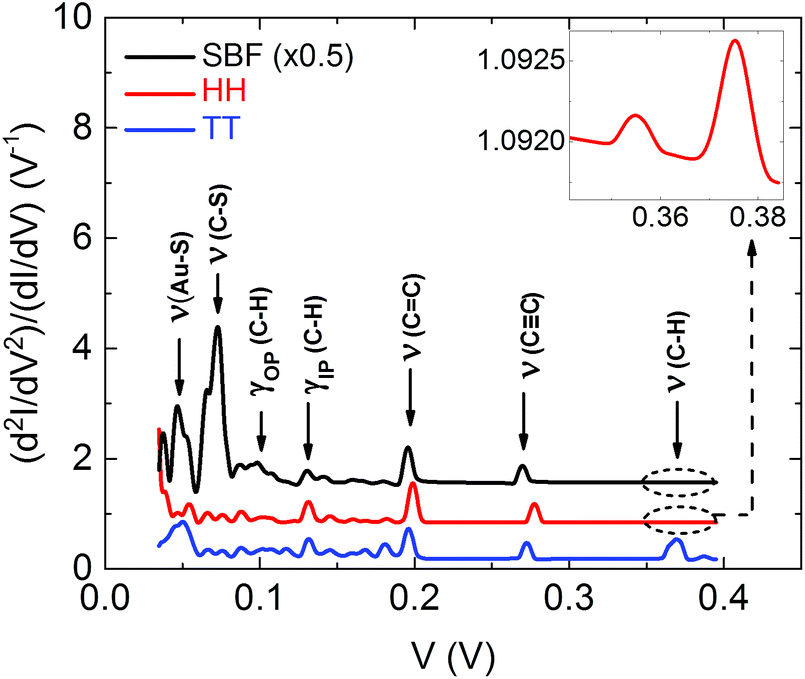 | ||
| Fig. 5 Calculated IET spectra for SBF, HH, and TT configurations. The spectra are offset for better visibility. The inset shows the magnified part of the IET spectrum for HH in the voltage range of 0.34 to 0.39 V, where the peaks have a lower intensity compared to the rest of the peaks and compared to the TT configuration. | ||
Conclusions
To summarize, we have presented a thorough characterization of the transport properties of single-molecule junctions of 9,9′-spirobifluorene, contacted to mechanically adjustable Au electrodes. The molecule features a tripodal footprint and an arm that is connected in the para position to the foot and that establishes a conjugated conduction path all the way from one of the legs to the end of the arm. When coupling this molecule via thiol end groups to the Au electrodes, a relatively high linear conductance of 10−3G0 is obtained. In view of the length of the molecular wire of 1.7 nm this implies a current path with a high degree of conjugation that is comparable to the one of the monopodal version of the molecule with a single leg. Our comprehensive data sets reveal that both the conductance values as well as their variation with stretching can be consistently explained by assuming a particular binding geometry, in which the conjugated foot and the arm are coupled to a single Au atom (TT) on either electrode. Besides a higher trapping rate of the tripodal version (20%) compared the monopodal version (8%), both molecules perform comparably well. Our findings also imply that the conductive arm encloses a finite angle with the surface, when deposited on a flat surface as required for scanning tunnelling microscope experiments. This property makes the spirobifluorene platform suitable for hosting functional units like switches, rectifiers or photosensitive moieties.Methods
Synthesis
Our synthetic strategy used for the preparation of the 2,7,3′,6′-tetrasubstituted 9,9′-spirobifluorene tripodal derivative 7 is outlined in Scheme 1. This approach is based on the assembly of two buildings blocks 3 and 4via a Sonogashira cross-coupling reaction. The synthesis of 4-ethynyl-1-[2-(trimethylsilyl)ethylsulfanyl]benzene 3, the first building block, started from 4-bromo-1-[2-(trimethylsilyl)ethylsulfanyl]benzene 1, which was coupled with trimethylsilylacetylene to afford a trimethylsilyl protected acetylene derivative 2. Subsequent cleavage of the trimethylsilyl protecting group under basic conditions afforded 3 in almost quantitative yield. With the previously prepared spirobifluorene derivative 4 in hand,17 the further functionalization via a Sonogashira cross-coupling reaction with acetylene derivative 3 chemoselectively provided substitution in position 7, which is based on the differential reactivity of iodine and bromine under the Pd catalysis. To introduce the third alkylsulphanyl group, spirobifluorene derivative 5 was treated with 2-(trimethylsilyl)ethanthiol in the presence of Pd2(dba)3, Xantphos and Hünig's base to provide the desired tripodal spirobifluorene 6 in 96% yield. Final transprotection of the thiol was successfully performed using AgBF4 and acetyl chloride in dichloromethane to obtain the desired tripodal thioacetate 7 in 73% yield. | ||
| Scheme 1 Synthesis of spirobifluorene derivative 7. Reagents and conditions: (i) trimethylsilylacetylene, PdCl2(PPh3)2, CuI, Et3N; (ii) K2CO3, MeOH, THF; (iii) 3, PdCl2(PPh3)2, CuI, Et3N; (iv) TMS(CH2)2SH, Pd2(dba)3, XPhos, iso-Pr2EtNH, dioxane, Δ; (v) AgBF4, AcCl, CH2Cl2. | ||
A similar strategy was used for the preparation of the monopodal fluorene derivative 12, which is outlined in Scheme 2. Methylation of 2-bromo-7-iodo-9H-fluorene 8 with methyl iodide in position 9 afforded 2-bromo-7-iodo-9,9-dimethylfluorene 9 in 89% yield. A subsequent Sonogashira cross-coupling reaction with acetylene derivative 3, and a following substitution of bromine with 2-(trimethylsilyl)ethanthiol provided the rod-like fluorene derivative 11 in almost quantitative yield. For the final transprotection of the 2-(trimethylsilyl)ethylsulphanyl groups of compound 11 to acetylsulfanyl groups, several alternative protocols have been used.
 | ||
| Scheme 2 Synthesis of fluorene derivative 12. Reagents and conditions: (i) (a) tert-BuOK, THF, (b) CH3I; (ii) 3, PdCl2(PPh3)2, CuI, Et3N; (iii) TMS(CH2)2SH, Pd2(dba)3, XPhos, iso-Pr2EtNH, dioxane, Δ; (iv) (a) TBAF, THF, (b) AcCl. | ||
But contrary to our previous results on spirobifluorene derivative 6, transprotection with AgBF4 and acetyl chloride (AcCl) in dichloromethane resulted in the complex mixture of acetylated products and side products, considerably reducing the yield of the desired product 12. Cleavage of the 2-(trimethylsilyl)ethyl protecting group has been successfully performed using tetrabutylammonium fluoride (TBAF), and the subsequent treatment with acetyl chloride afforded the desired monopodal thioacetate 12 in 53% yield.
The presence of a terminal thioacetate group allows the target tripodal 7 and monopodal 12 molecules to be bound to a gold surface. The acetyl works as a labile thiol protecting group and can mildly and efficiently be cleaved prior to the physical investigations or in situ upon binding to the gold surface. Further details and the NMR spectra of 7 and 12 are given in section 1 of the ESI.†
Device fabrication
The process of sample fabrication is as follows. The softly polished bronze wafer (diameter 60 mm, thickness 270 μm) is covered by a spin-coated layer of polyimide (thickness ∼2 μm), which serves as an electrical insulator and a sacrificial layer in the subsequent etching process. In order to polish the bronze wafer, two different grain sizes of sand paper are used, and then the wafer is polished again using a polishing paste. The spin-coated polyimide is baked at 430 °C for 100 min in vacuum. On top of these prepared wafers, a double layer of electron-beam resists (ER), MMA-MAA/PMMA, is deposited by spin-coating. Prior to performing the electron beam lithography (EBL) process, the wafer is cut into proper dimension (4 × 19 mm2). After developing, gold of about 80 nm thick is deposited using electron beam evaporation at a pressure of about 10−8 mbar. Finally, in order to form a free-standing bridge, the samples are installed in a vacuum chamber of a reactive ion etcher (RIE). Oxygen (O2) removes about 700 nm of the polyimide layer in microwave plasma of 50 W in oxygen flow of 50 ccm for 30 min.Deposition of molecules
After the etching procedure, the dilute solution of molecules (14.7 mg in 5 mL tetrahydrofurane (THF)) is prepared, and then one droplet of ammonium hydroxide (NH4OH) is added to the solution to deprotect the acetyle group.45,46 We obtained similar results by using triethylamine (Et3N) for deprotection. The chemical drawing of the molecule is shown in Fig. 6. After deprotection, the patterned substrates were immersed in the molecular solution for 5 hours. Each sample was then rinsed with a few milliliters of THF and gently blown dry in a stream of nitrogen gas to remove noncovalently-attached molecules from the metal surface. This method is called formation of a self-assembled monolayer (SAM), although it cannot be checked with our methods, whether in fact a single and complete monolayer is formed.37,47 | ||
| Fig. 6 Ground state geometry of the SBF molecule (C41H28S4O4). The acetyle end groups are removed with one droplet of ammoniumhydroxide (NH4OH) or triethylamine (Et3N). | ||
Low temperature setup
Charge transport measurements through single molecules were carried out in a custom-designed cryogenic vacuum insert equipped with a MCBJ. The devices are mounted into the break mechanism inside an inner vacuum chamber which is evacuated and purged with He gas before being immersed into a liquid He dewar. The breaking mechanics is controlled by a dc motor with a gear box (reduction ratio of 1![[thin space (1/6-em)]](https://www.rsc.org/images/entities/char_2009.gif) :1734) connected with a vacuum feed-through. In order to reduce the electronic noise level, all measurement lines inside the cryostat are carefully filtered using home-made coaxial cables and SMA connectors. Inside the inner vacuum chamber, the sample holder part is shielded again with a copper can to eliminate the influence of electromagnetic fields.40
:1734) connected with a vacuum feed-through. In order to reduce the electronic noise level, all measurement lines inside the cryostat are carefully filtered using home-made coaxial cables and SMA connectors. Inside the inner vacuum chamber, the sample holder part is shielded again with a copper can to eliminate the influence of electromagnetic fields.40
Transport measurements
The conductance measurements of opening and closing were performed by a sub-femtoamp source-meter (Keithley 6430) operating with an automatic variable gain pre-amplifier. In order to measure the I–V curves, we used a programmable dc source (Yokogawa 7651) and a low-noise current amplifier (Femto DLPCA-200) followed by a digital multimeter (Keithley 2000). Every grounds of the system were carefully designed to avoid ground-loops and electrical noise. All data were collected by a Labview software through GPIB cables. The differential conductance (dI/dV) and its derivative (d2I/dV2) were measured simultaneously as first and second harmonic signals using twin lock-in amplifiers (Stanford Research Systems 830) followed by two digital multimeters,37 as illustrated in Fig. S20 in the ESI.† A DC bias added to an AC modulation of 5 mV (root-mean-square) at a frequency of 1642 Hz was applied to the sample. The normalized IET spectra, (d2I/dV2/(dI/dV)), were obtained in real time to cancel the effect of junction distance changes while monitoring the signals by the synchronized lock-in amplifiers.Electronic structure calculations
To model the geometric and electronic properties of the SBF-based molecular junctions, we use DFT as implemented in the TURBOMOLE software package48 with the PBE generalized gradient exchange–correlation functional.49–52 As the basis set we employ def-SV(P),53–55 which is of split valence quality. Total energies are converged to a precision of better than 10−6 atomic units, and structure optimizations are carried out until the maximum norm of the Cartesian gradients has fallen below values of 10−5 atomic units. To determine the junction geometries we proceed as described in ref. 28 by first connecting the molecule to one electrode, optimizing the structure and then connecting the molecule to the other electrode in a symmetric manner. Then the junction except for the outermost gold layers is relaxed. In this way we obtain approximate equilibrium geometries for the molecular junctions.Vibrational modes and EVIB couplings are determined after the geometry optimization by using the “aoforce” and “evib” modules of TURBOMOLE43,56 based on accurate analytical derivative techniques. We assume that the “dynamical region” of the molecular junction, i.e. the region where the atoms are allowed to vibrate, is identical to its relaxed part, while we assign an infinite mass to the fixed atoms. We characterize the modes by considering the displacement vectors. Due to the larger number of atoms, which are free to vibrate, and since symmetries are generally absent, the classification of vectors remains approximate only.
Transport calculations
Using the DFT+Σ derived electronic structure,27,57 we determine the elastic transport properties of the molecular contacts in the framework of the Landauer–Büttiker formalism with the help of Green's function techniques.28,42–44 The inelastic effects are taken into account in a LOE of the electric current in terms of the EVIB coupling. In the procedure the EVIB couplings, as determined from DFT, are used together with the DFT+Σ corrected one to keep the elastic transport unchanged. For the calculation of the theoretical IET spectra within the wide-band limit (WBL) we assumed a temperature of T = 4.2 K and a vibrational broadening of 1 meV that describes the intrinsic line-width broadening of the IET signals due to a finite temperature and finite life-time of the vibrational modes, respectively. In addition, following the experiments, the spectra are additionally broadened by an AC voltage VAC = 5 meV.Acknowledgements
We enjoyed fruitful interactions with M. Lukas, L. Gerhard, R. Hayakawa, and W. Wulfhekel. We gratefully acknowledge financial support from the research network “Functional Nanostructures” funded by the Baden-Württemberg Foundation, the Helmholtz Research Program STN (Science and Technology of Nanosystems), the Carl-Zeiss Foundation, and the German Research Foundation (DFG) through Collaborative Research Center (SFB) 767. Important part of the numerical modeling was carried out on the computational resources of the bwHPC program, namely the bwUniCluster and the JUSTUS HPC facility.Notes and references
- J. C. Cuevas and E. Scheer, Molecular Electronics: An Introduction to Theory and Experiment, World Scientific, Singapore, 2010 Search PubMed.
- S. Aradhya and L. Venkataraman, Nat. Nanotechnol., 2013, 8, 399–410 CrossRef CAS PubMed.
- M. Valášek, M. Lindner and M. Mayor, Beilstein J. Nanotechnol., 2016, 7, 374–405 CrossRef.
- Y. Ie, T. Hirose, H. Nakamura, M. Kiguchi, N. Takagi, M. Kawai and Y. Aso, J. Am. Chem. Soc., 2011, 133, 3014–3022 CrossRef CAS PubMed.
- M. Lukas, K. Dössel, A. Schramm, O. Fuhr, C. Stroh, M. Mayor, K. Fink and H. v. Löhneysen, ACS Nano, 2013, 7, 6170–6180 CrossRef CAS PubMed.
- S. Katano, Y. Kim, H. Matsubara, T. Kitagawa and M. Kawai, J. Am. Chem. Soc., 2007, 129, 2511–2515 CrossRef CAS PubMed.
- F. L. Otte, S. Lemke, C. Schütt, N. R. Krekiehn, U. Jung, O. M. Magnussen and R. Herges, J. Am. Chem. Soc., 2014, 136, 11248–11251 CrossRef CAS PubMed.
- Y. Ie, K. Tanaka, A. Tashiro, S. K. Lee, H. R. Testai, R. Yamada, H. Tada and Y. Aso, J. Phys. Chem. Lett., 2015, 6, 3754–3759 CrossRef CAS PubMed.
- T. Kitagawa, Y. Idomoto, H. Matsubara, D. Hobara, T. Kakiuchi, T. Okazaki and K. Komatsu, J. Org. Chem., 2006, 71, 1362–1369 CrossRef CAS PubMed.
- Y. Shirai, L. Cheng, B. Chen and J. M. Tour, J. Am. Chem. Soc., 2006, 128, 13479–13489 CrossRef CAS PubMed.
- D. Takamatsu, Y. Yamakoshi and K. Fukui, J. Phys. Chem. B, 2006, 110, 1968–1970 CrossRef CAS PubMed.
- L. Wei, K. Padmaja, W. J. Youngblood, A. B. Lysenko, J. S. Lindsey and D. F. Bocian, J. Org. Chem., 2004, 69, 1461–1469 CrossRef CAS PubMed.
- S. Ramachandra, K. C. Schuermann, F. Edafe, P. Belser, C. A. Nijhuis, W. F. Reus, G. M. Whitesides and L. De Cola, Inorg. Chem., 2011, 50, 1581–1591 CrossRef CAS PubMed.
- D. Hirayama, K. Takimiya, Y. Aso, T. Otsubo, T. Hasobe, H. Yamada, H. Imahori, S. Fukuzumi and Y. Sakata, J. Am. Chem. Soc., 2002, 124, 532–533 CrossRef CAS PubMed.
- B. Baisch, D. Raffa, U. Jung, O. M. Magnussen, C. Nicolas, J. Lacour, J. Kubitschke and R. Herges, J. Am. Chem. Soc., 2009, 131, 442–443 CrossRef CAS PubMed.
- K.-Y. Chen, O. Ivashenko, G. T. Carroll, J. Robertus, J. C. M. Kistemaker, G. London, W. R. Browne, P. Rudolf and B. L. Feringa, J. Am. Chem. Soc., 2014, 136, 3219–3224 CrossRef CAS PubMed.
- M. Valášek, K. Edelmann, L. Gerhard, O. Fuhr, M. Lukas and M. Mayor, J. Org. Chem., 2014, 79, 7342–7357 CrossRef PubMed.
- H. Vazquez, R. Skouta, S. Schneebeli, M. Kamenetska, R. Breslow, L. Venkataraman and M. S. Hybertsen, Nat. Nanotechnol., 2012, 7, 663–667 CrossRef CAS PubMed.
- Y. Kim, A. Garcia-Lekue, D. Sysoiev, T. Frederiksen, U. Groth and E. Scheer, Phys. Rev. Lett., 2012, 109, 226801 CrossRef PubMed.
- W. Hong, D. Z. Manrique, P. Moreno-García, M. Gulcur, A. Mishchenko, C. J. Lambert, M. R. Bryce and T. Wandlowski, J. Am. Chem. Soc., 2012, 134, 2292–2304 CrossRef CAS PubMed.
- R. Frisenda, S. Tarkuç, E. Galán, M. L. Perrin, R. Eelkema, F. C. Grozema and H. S. J. van der Zant, Beilstein J. Nanotechnol., 2015, 8, 1558–1567 CrossRef PubMed.
- H. Lissau, R. Frisenda, S. T. Olsen, M. Jevric, C. R. Parker, A. Kadziola, T. Hansen, H. S. J. van der Zant, M. B. Nielsen and K. V. Mikkelsen, Nat. Commun., 2016, 6, 10233 CrossRef PubMed.
- N. Agrait, A. Levy Yeyati and J. M. van Ruitenbeek, Phys. Rep., 2003, 377, 81–279 CrossRef CAS.
- M. Paulsson, C. Krag, T. Frederiksen and M. Brandyge, Nano Lett., 2009, 9, 117–121 CrossRef CAS PubMed.
- F. Schwarz, G. Kastlunger, F. Lissel, H. Riel, K. Venkatesan, H. Berke, R. Stadler and E. Lörtscher, Nano Lett., 2014, 14, 5932–5940 CrossRef CAS PubMed.
- L. A. Zotti, T. Kirchner, J. C. Cuevas, F. Pauly, T. Huhn, E. Scheer and A. Erbe, Small, 2010, 6, 1529–1535 CrossRef CAS PubMed.
- L. A. Zotti, M. Bürkle, F. Pauly, W. Lee, K. Kim, W. Jeong, Y. Asai, P. Reddy and J. C. Cuevas, New J. Phys., 2014, 16, 015004 CrossRef.
- F. Pauly, J. K. Viljas, U. Huniar, M. Häfner, S. Wohlthat, M. Bürkle, J. C. Cuevas and G. Schön, New J. Phys., 2008, 10, 125019 CrossRef.
- M. Paulsson and M. Brandbyge, Phys. Rev. B: Condens. Matter, 2007, 76, 115117 CrossRef.
- M. Bürkle, J. K. Viljas, D. Vonlanthen, A. Mishchenko, G. Schön, M. Mayor, T. Wandlowski and F. Pauly, Phys. Rev. B: Condens. Matter, 2012, 85, 075417 CrossRef.
- H. Weber, J. Reichert, F. Weigend, R. Ochs, D. Beckmann, M. Mayor, R. Ahlrichs and H. v. Löhneysen, Chem. Phys., 2002, 281, 113–125 CrossRef CAS.
- Y. Kim, T. Pietsch, A. Erbe, W. Belzig and E. Scheer, Nano Lett., 2011, 11, 3734–3738 CrossRef CAS PubMed.
- S. Guo, J. Hihath, I. Díez-Pérez and N. Tao, J. Am. Chem. Soc., 2011, 133, 19189–19197 CrossRef CAS PubMed.
- C. M. Guédon, H. Valkenier, T. Markussen, K. S. Thygesen, J. C. Hummelen and S. J. van der Molen, Nat. Nanotechnol., 2012, 7, 305–309 CrossRef PubMed.
- W. Wang, T. Lee, I. Kretzschmar and M. A. Reed, Nano Lett., 2004, 4, 643–646 CrossRef CAS.
- A. Troisi and M. A. Ratner, Nano Lett., 2006, 6, 1784–1788 CrossRef CAS PubMed.
- Y. Kim, H. Song, F. Strigl, H. F. Pernau, T. Lee and E. Scheer, Phys. Rev. Lett., 2011, 106, 196804 CrossRef PubMed.
- M. A. Karimi, S. G. Bahoosh, M. Herz, R. Hayakawa, F. Pauly and E. Scheer, Nano Lett., 2016, 16, 1803–1807 CrossRef CAS PubMed.
- J. G. Kushmerick, J. Lazorcik, C. H. Patterson, R. Shashidhar, D. S. Seferos and G. C. Bazan, Nano Lett., 2004, 4, 639–642 CrossRef CAS.
- L. H. Yu, C. D. Zangmeister and J. G. Kushmerick, Phys. Rev. Lett., 2007, 98, 206803 CrossRef PubMed.
- T. Böhler, A. Edtbauer and E. Scheer, Phys. Rev. B: Condens. Matter, 2007, 76, 125432 CrossRef.
- T. Frederiksen, M. Paulsson, M. Brandbyge and A.-P. Jauho, Phys. Rev. B: Condens. Matter, 2007, 75, 205413 CrossRef.
- M. Bürkle, J. K. Viljas, T. J. Hellmuth, E. Scheer, F. Weigend, G. Schön and F. Pauly, Phys. Status Solidi B, 2013, 250, 2468–2480 CrossRef.
- J. K. Viljas, J. C. Cuevas, F. Pauly and M. Häfner, Phys. Rev. B: Condens. Matter, 2005, 72, 245415 CrossRef.
- H. Valkenier, E. H. Huisman, P. A. van Hal, D. M. de Leeuw, R. C. Chiechi and J. C. Hummelen, J. Am. Chem. Soc., 2011, 133, 4930–4939 CrossRef CAS PubMed.
- M. T. González, E. Leary, R. García, P. Verma, M. A. Herranz, G. Rubio-Bollinger, N. Martin and N. Agraït, J. Phys. Chem. C, 2011, 115, 17973–17978 Search PubMed.
- Y. Kim, T. J. Hellmuth, M. Bürkle, F. Pauly and E. Scheer, ACS Nano, 2011, 5, 4104–4111 CrossRef CAS PubMed.
- R. Ahlrichs, M. Bär, M. Häser, H. Horn and C. Kölmel, Chem. Phys. Lett., 1989, 162, 165–169 CrossRef CAS.
- P. A. M. Dirac, Proc. R. Soc. London, Ser. A, 1929, 123, 714–733 CrossRef CAS.
- J. C. Slater, Phys. Rev., 1951, 81, 385–390 CrossRef CAS.
- J. P. Perdew and Y. Wang, Phys. Rev. B: Condens. Matter, 1992, 45, 13244–13249 CrossRef.
- J. P. Perdew, K. Burke and M. Ernzerhof, Phys. Rev. Lett., 1996, 77, 3865–3868 CrossRef CAS PubMed.
- A. Schäfer, H. Horn and R. Ahlrichs, J. Chem. Phys., 1992, 97, 2571–2577 CrossRef.
- K. Eichkorn, O. Treutler, H. Öhm, M. Häser and R. Ahlrichs, Chem. Phys. Lett., 1995, 242, 652–660 CrossRef CAS.
- K. Eichkorn, F. Weigend, O. Treutler and R. Ahlrichs, Theor. Chem. Acc., 1997, 97, 119–124 CrossRef CAS.
- P. Deglmann, K. May, F. Furche and R. Ahlrichs, Chem. Phys. Lett., 2004, 384, 103–107 CrossRef CAS.
- S. Y. Quek, L. Venkataraman, H. J. Choi, S. G. Louie, M. S. Hybertsen and J. B. Neaton, Nano Lett., 2007, 7, 3477–3482 CrossRef CAS PubMed.
Footnote |
| † Electronic supplementary information (ESI) available. See DOI: 10.1039/c5nr08708b |
| This journal is © The Royal Society of Chemistry 2016 |