
 Open Access Article
 This Open Access Article is licensed under a
 Creative Commons Attribution 3.0 Unported Licence
Tunable charge transfer properties in metal-phthalocyanine heterojunctions†
P. F.
Siles
*ab,
T.
Hahn
c,
G.
Salvan
d,
M.
Knupfer
b,
F.
Zhu
ab,
D. R. T.
Zahn
def and
O. G.
Schmidt
abef
aMaterial Systems for Nanoelectronics, Technische Universität Chemnitz, 09107 Chemnitz, Germany. E-mail: p.r.siles@ifw-dresden.de
bInstitute for Integrative Nanosciences, IFW Dresden, 01069 Dresden, Germany
cInstitute of Theoretical Physics, TU Bergakademie Freiberg, 09696 Freiberg, Germany
dSemiconductor Physics, Technische Universität Chemnitz, 09107 Chemnitz, Germany
eCenter for Advancing Electronics Dresden (cfAED), TU Dresden, 01062 Dresden, Germany
fFaculty of Mechanical Engineering, Cluster of Excellence MERGE, Technische Universität Chemnitz, 09107 Chemnitz, Germany
First published on 30th March 2016
Abstract
Organic materials such as phthalocyanine-based systems present a great potential for organic device applications due to the possibility of integrating films of different organic materials to create organic heterostructures which combine the electrical capabilities of each material. This opens the possibility to precisely engineer and tune new electrical properties. In particular, similar transition metal phthalocyanines demonstrate hybridization and charge transfer properties which could lead to interesting physical phenomena. Although, when considering device dimensions, a better understanding and control of the tuning of the transport properties still remain in the focus of research. Here, by employing conductive atomic force microscopy techniques, we provide an insight about the nanoscale electrical properties and transport mechanisms of MnPc and fluorinated phthalocyanines such as F16CuPc and F16CoPc. We report a transition from typical diode-like transport mechanisms for pure MnPc thin films to space-charge-limited current transport regime (SCLC) for Pc-based heterostructures. The controlled addition of fluorinated phthalocyanine also provides highly uniform and symmetric-polarized transport characteristics with conductance enhancements up to two orders of magnitude depending on the polarization. We present a method to spatially map the mobility of the MnPc/F16CuPc structures with a nanoscale resolution and provide theoretical calculations to support our experimental findings. This well-controlled nanoscale tuning of the electrical properties for metal transition phthalocyanine junctions stands as key step for future phthalocyanine-based electronic devices, where the low dimension charge transfer, mediated by transition metal atoms could be intrinsically linked to a transfer of magnetic moment or spin.
1. Introduction
The charge transport characteristics of organic molecules as well as the ability to control and properly modify these electrical properties represent a key foundation for the field of molecular electronics and the development of novel organic-based electronic devices. The controlled addition or removal of charges from particular molecules, and the molecule–molecule or molecule–substrate charge transfer stand as an effective method to modify or engineer the physical properties of materials. In addition, the diversity of molecular systems and the flexibility of molecular synthesis have provided a valuable freedom to design functional molecular systems that offer a plethora of device applications. Potential candidates for memory devices were reported utilizing organo-metallic complexes of TCNQ (tetracyanoquinodimethane),1,2 metal-phthalocyanines multilayers3 and ZMP (zinc methyl phenalenyl).4 Organic tailored battery materials5 with high capacity capabilities, molecular magnets,6 spin-filter molecules7 and single molecule8 or thin film-based field-effect transistors9–11 are examples of the demonstrated diversity of applications, where interface and charge transfer effects represent a common cornerstone. A wide spectrum of physical phenomena also appears when heterostructures of different organic materials are properly engineered. For example, the formation of a two-dimensional metallic interface was possible due to the charge transfer between two insulating organic crystals.12–14 Also, metal–insulator transitions15 and even superconductivity16,17 were reported when charge transfer organic crystals are formed by combining strong electron accepting with strong electron donating organic molecules. This provides favorable possibilities to control the performance of organic electronic devices. For instance, it is possible to enhance the charge carrier injection from electrodes by including organic dopants in organic semiconductors,18 and to tune hole injection barriers at organic junctions by modifying the electrode surfaces with particular organic layers.19Recently, a heterostructure of manganese-phthalocyanine (MnPc) and fluorinated cobalt-phthalocyanine (F16CoPc), two structurally similar transition metal phthalocyanines, demonstrated the occurrence of hybridization and was proved to present a local charge transfer which affects only the transition metal centers.20 Here, the change of the transition metal charge state is directly related to a change of the respective magnetic moment. Therefore, such phthalocyanine-based junction may lead to new and interesting physical phenomena where the low dimensional charge transfer, mediated by transition metal atoms, is intrinsically linked to a transfer of magnetic moment or spin. This is also supported by further studies which indicated the filling of the Co 3dz2 orbital due to the charge transfer at the interface to MnPc.21 A blend of these organic materials also showed that a bulk material can be formed. These blends maintain the charge and spin transfer between the two molecules, and showed a new energy electronic excitation, affecting its optical properties.22 Nevertheless, an exhaustive study of the electronic and magnetic properties of this phthalocyanine junction system is still required. Despite the existence of detailed structural analysis and theoretical studies supporting the charge transfer characteristics of these junctions,20–22 to the best of our knowledge, a better understanding of the transport properties at the nanoscale for these metal-phthalocyanine systems is still a conundrum due to the little experimental evidence reported.
In this work, conductive scanning probes techniques are employed to systematically study the transport properties of phthalocyanine-based junctions. In particular, atomic force microscopy (AFM) transport techniques represent nowadays a well-established tool for local electrical investigations of a growing spectrum of organic materials.23–29 The precise manipulation and control of a conducting AFM probe allows preserving the integrity of the organic structures by eliminating the need of sputtering or thermal depositions for preparation of top electrodes,30 which for the thickness range investigated in this work would inevitably compromise the integrity of the organic films and even lead to short circuit issues. By using current sensing AFM (cs-AFM), we investigate and identify transport mechanisms through the organic materials. Two different approaches are implemented here via AFM conductive methods. On one side, the electrical current mapping provides a spatial micro-scale view of the electrical properties of the organic systems. On the other side, the local I–V spectroscopy characterization allows the transport properties to be explored at the nanoscale limit of the AFM probe dimensions. We engineer the charge transport properties of MnPc thin films by the controlled addition of fluorinated metal-phthalocyanine thin films. Since charge transfer affects the energy level alignment and therefore the transport behavior, these phthalocyanine-based junctions offer great potential for the application of such interfaces in organic electronic devices. Assuming similar interaction for other flat transition metal complexes, we investigate two different molecule pairs. Hence, heterojunctions of MnPc with F16CuPc and also MnPc with F16CoPc are considered in this contribution.
2. Results and discussion
2.1 Metal-phthalocyanine heterojunctions
Initially, the local transport properties of MnPc films on Co substrates are investigated as a function of the thickness of the organic film. Here, an organic layer stack of 10 nm is defined as reference in order to investigate the effect on the transport properties due to the addition of fluorinated phthalocyanines on the MnPc thin films. Therefore, a MnPc thin film of 10 nm deposited on a cobalt (Co) substrate is defined as reference sample (sample A). While the total thickness of 10 nm is kept constant, different organic heterostructures are engineered by introducing thin film layers of F16CuPc and F16CoPc, with a specific thickness, to the reference MnPc film (see Fig. 1b). In this way, the transport properties of the organic heterostructures are explored as a function of the concentration of fluorinated metal-phthalocyanine. As shown in Fig. 1b, 50% of F16CuPc (sample B) and 25% of F16CuPc (sample C) are considered. The variations of the electrical response due to the arranging of the energy levels in the organic heterostructure structure are also studied by controlling the location of the fluorinated organic film in the heterostructure (sample D). Finally, in order to explore the influence of the metallic center of the fluorinated compound on the tuning of the transport properties, a sample with 50% of F16CoPc (sample E) is also prepared, following identical structural characteristics as sample B. | ||
| Fig. 1 Experimental set up and organic heterostructure configurations. (a) Sketch of the cs-AFM set up for local transport measurements. (b) Phthalocyanine heterostructures: sample A (10 nm MnPc), sample B (5 nm F16CuPc/5 nm MnPc), sample C (2.5 nm F16CuPc/7.5 nm MnPc), sample D (5 nm MnPc/5 nm F16CuPc) and sample E (5 nm F16CoPc/5 nm MnPc). All samples are deposited with a Co bottom electrode of 20 nm. The table provides the thicknesses for each layer in the samples. | ||
2.2 Tuning transport properties via organic doping
The topography characteristics of organic films play an important role in the transport properties at the nanoscale. For example, structural defects may be induced due to the typical grain-like arrangement of thin films of metal-phthalocyanines. These defects may drive the transport response of the organic material in a device scale. This becomes of special interest when thin films of different organic materials are employed to create an organic heterostructure that combines the electrical capabilities of each material in order to precisely tune new electrical properties. Our choice of organic materials is motivated by the possibility of charge transfer properties previously demonstrated and by the fact that transition metal phthalocyanines represent an important model of a broad class of planar metal–organic compounds with interesting magnetic properties31,32 due to the d orbitals of the metallic center of the molecules which are partially empty. Here, by analyzing both the morphology as well as the electronic characteristics of the phthalocyanine-based heterostructures, we provide experimental evidence of the tuning and enhancement of the transport properties of a metal phthalocyanine-based heterostructure by accurately manipulating the constituent organic thin films such as F16CuPc and MnPc.Since the interfacial and thin film properties of the organic materials are strongly related to the molecule–molecule interactions and interactions of the molecules with the underlying substrate, we performed an AFM investigation via spatial current mapping, which allows correlating the topography characteristics of the organic materials with its transport properties. Fig. 2a shows the topography characteristics for each component layer of the organic heterostructure as well as for the Co substrate. A typical grain-like morphology with average grain radius of 11.0 nm and 12.6 nm, and average grain heights of 1.9 nm and 1.0 nm, was observed for the F16CuPc and MnPc organic layers respectively. Also, an average roughness (rms) of 1.7 nm, 1.1 nm and 0.6 nm were obtained for the case of F16CuPc, MnPc and the Co bottom electrode, respectively (see ESI S1†). By performing AFM current mapping of the MnPc organic films as a function of its thickness (see Fig. 2b for the case of −3 V) a minimum thickness of 10 nm (sample A) is determined which provides the maximum electrical signal while maintaining an adequate structural and electrical stability of the material (see ESI S2† for more details).
 | ||
| Fig. 2 Topography and dynamic transport analysis of phthalocyanine organic heterojunctions. (a) AFM topography characteristics for Co substrate, MnPc and F16CuPc thin films. (b) Thickness dependence of current maps for MnPc thin films obtained at −3 V. (c) Current maps for F16CuPc/MnPc bilayer structures (samples B and C) obtained at −1.5 V. Current map inset shows a zoom-in detail for an area of 1.5 × 1.5 μm2 with a higher current scale resolution. Current versus distance inset represents an average current profile for each sample. Due to the strong current dependence on the thickness of the organic material, all current maps are presented in a logarithmic scale. All current scales are presented in absolute value. (d) Electrical profile for the normalized distributions of conducting sites on organic films for samples A–D. | ||
Besides the dependence on the thickness of the organic films, the transport current on MnPc thin films appears to be highly driven by the grain-like structure of the films, as shown in Fig. 2b, where locations of higher electrical current are observed to match with the location of the organic grains in the corresponding topography image (not shown here). The AFM topography analysis may suggest a different arrangement of the F16CuPc and MnPc molecules during the thermal deposition process, which is also reflected in the electrical response of the organic films. Even though the fluorinated films present higher grain dimensions, MnPc grains are wider and present a higher dispersion of spatial dimensions. This may induce a higher number of defects in the organic films at the nanoscale, which directly affect the local transport properties. This is also supported by the more uniform transport characteristics of the fluorinated CuPc films in comparison with the MnPc films (see current maps in Fig. 2). The addition of the fluorinated phthalocyanine films in the organic structure plays an important role for tuning (lowering) its energy bands, as shown for similar organic systems.20 Here we add a concentration of 25% and 50% of F16CuPc to the 10 nm thick MnPc-based organic structures, which total thickness is always kept constant (see sample B and sample C in Fig. 1). The fluorinated phthalocyanine film between the Co electrode and the MnPc film provides an adequate re-alignment of the energy bands of the organic structure in such a way that an enhancement of the charge carrier transfer from the Co electrode to the organic films is enabled. A gradual inclusion of the fluorinated CuPc film provides a higher and more uniform electrical response of the organic heterostructure, as shown in Fig. 2c. Here, only half of the applied voltage (therefore smaller electric field) is required in order to obtain similar electric current levels as the ones obtained for the 10 nm thick reference MnPc sample (see Fig. 2b and c). The current profile in Fig. 2c indicates typical electric current values when a 25% and a 50% of F16CuPc compose the organic heterostructure. An average electrical current of 3.92 nA is obtained for a pure-MnPc 10 nm thick sample (sample A) when a voltage of −3 V is applied. On the other hand, average current values of 2.92 nA and 4.74 nA are obtained when 2.5 nm (sample B) or 5 nm (sample C) of F16CuPc are included in the structure and a voltage of −1.5 V is applied. Taking advantage of the dynamic AFM electrical studies, one can explore the homogeneity of the spatial transport properties by obtaining the conductance dependence of the normalized distribution of conducting sites in the current maps.28 Heterostructures containing fluorinated phthalocyanine films show a highly uniform electrical conductance for the totality of conducting sites over the areas considered (5 × 5 μm2). On the other hand, films containing only MnPc have a distribution of conductance which slightly varies with the conducting sites. Less than 10% of the sites have a higher conductance with respect to the majority of sites (see Fig. 2d). It is worth to point out that although the electronic characteristics appear to be more uniform when the fluorinated film is included in the organic structure (see Fig. 2b and c), at the nanoscale, the films still preserve their grain-dependent transport characteristics (see detail in current map inset in Fig. 2c). When performing dynamic transport characterization, the AFM probe maps the sample surface within steps of about 9–10 nm, while a constant voltage is applied. Once the typical grain dimensions of the organic films have radii between 11–12 nm, spatial current mapping provides a good correlation of the topography of the grain morphology characteristics and the electrical response. A proper validation of the dynamic AFM electrical investigations should include information of the electrical current signal when no voltage is applied at the organic interface as well as a constant monitoring of the AFM probe force load on the organic substrate. This ensures no influence of external conditions such as probe-sample friction or variations of force which may induce undesirable modifications of the electrical signal (see detailed information in ESI S2a and S2b†).
In order to further study the transport characteristics of the phthalocyanine-based heterostructures, we performed AFM local I–V spectroscopy which allows exploring a wider range of applied voltage and ultimately provides the possibility of determining transport mechanisms through the organic material. In Fig. 3, local spectroscopy was employed to investigate the I–V response of the organic films. A voltage range of ±3 V and a total organic structure thickness of 10 nm were defined as ideal conditions in order to ensure structural and electrical stability of the phthalocyanine-based films (see Fig. 3a and ESI S3†). The spectroscopy data presented here for all the samples correspond to an average of about 40 I–V cycles, where the probe-sample force interaction is continuously monitored and kept constant in order to ensure the reliability of the transport investigations (see ESI S2c†). Due to the typical contact area between probe and sample we are able to study the transport characteristics down to the nanoscale, limited only by the typical AFM probe dimensions. Considering the average grain dimensions of the organic films and the characteristics of the AFM probe, the electrical response via local I–V spectroscopy is plausible to consider the contribution of a few grains on the sample surface. Several I–V cycles were performed for all the heterostructure samples on several different locations of the surface of the organic film showing a highly symmetric and reproducible electrical response (see Fig. 3). As expected, the electrical transport through the organic films (see Fig. 3a for the case of MnPc films) is highly dependent on its thickness. We observe an exponential decrease of the conductance (G) of the MnPc films as a function of its thickness (see inset in Fig. 3a). This attenuation of the transport properties of the molecular films results to be independent of the applied voltage and may suggest a trapping or localization process of the charge carriers through the organic films, which leads to a reduction of the charge mobility. As shown in Fig. 3a, a threshold voltage for the activation of the transport properties is observed for the MnPc thin films and the on-set voltage increases with the thickness of the organic film. This behavior is in agreement with transport characteristics previously reported for other organic systems such as metalloporphyrins28 and other metal phthalocyanine molecules with metal centers such as Cu, Ni, Al and Mg.27,33–35
 | ||
| Fig. 3 Current–voltage behavior for phthalocyanine-based heterojunctions, obtained via local AFM I–V spectroscopy. (a) Electrical characteristics for MnPc thin films with a thickness of 10 nm (sample A), 20 nm and 35 nm. Dashed lines indicate the threshold voltage where the thinner organic film (10 nm) suffers an electrical breakdown (see also ESI S3†). The inset shows the conductance (G) of the films as a function of its thickness for |3 V|, |2.5 V| and |2 V|, as indicated by the green, dark red and blue arrows, respectively. For the inset, filled data points correspond to positive voltages and un-filled data points correspond to negative voltages. (b) Dependence of the local electrical response with the addition of F16CuPc. Inset highlights the high symmetry of the transport properties with the applied bias. All I–V curves shown represent an average of about 40 I–V cycles over different locations of the organic films. | ||
In addition, we explore the tuning of the energy bands of the organic structure by a controlled incorporation of fluorinated CuPc into the structure. As shown in Fig. 1b, the F16CuPc film is deposited in situ, between the Co bottom electrode and the MnPc film (samples B and C). For comparison, another sample where the order of F16CuPc and MnPc films is inverted (sample D) was also prepared. We observed a significant enhancement of the transport characteristics for the heterostructure samples as the concentration of F16CuPc increases (see Fig. 3b). Also, as the F16CuPc material is incorporated into the structure the organic structure becomes highly conductive, even for low voltages. In the case of the structure with 50% of F16CuPc (sample B) no on-set voltage is observed. The I–V characteristics appear to be highly symmetric with the applied voltage, as shown in the inset in Fig. 3b. Minor variations in the electrical response could be attributed to material structure asymmetries once that the bottom electrode is Co and the top electrode is the Pt-coated AFM probe. Interestingly, once the organic layers are reversed (see sample D), the mobility of the charge carriers through the heterostructure decreases and the overall transport characteristics of the structure are dramatically reduced. A higher rectification mechanism appears to dominate the transport characteristics, which seems to be driven by a poorer charge injection at the interface between the Co electrode and the MnPc thin film.
2.3 Dominant transport mechanisms and charge carrier mobility in F16CuPc/MnPc heterojunctions
In order to further investigate the dominant transport mechanism of the organic structures and taking advantage of the symmetric electrical response, we consider the region of positive bias for the case of sample A (100% MnPc) and sample B (50% F16CuPc and 50% MnPc) as shown in Fig. 4. Here, the current density (J) of the organic structures is presented as a function of the applied voltage. Due to the especial characteristics of the top electrode, i.e. AFM probe, we follow here the same approach previously reported for other organic systems.24,29 For the particular case of the Pt-coated hemispherical AFM probes used here, a probe-sample contact area with a radius of 14 nm is considered, assuming a typical probe indentation of 1 nm over the organic surface. This is reasonable when considering the well-controlled and low probe force load of 2 nN maintained along all the AFM-based electrical measurements (see also ESI S2c†). | ||
| Fig. 4 Transport mechanisms for metal phthalocyanine-based heterostructures. Solid lines represent the average of about 40 I–V cycles for sample A (black) and sample B (blue). Red dotted line corresponds to a diode-like transport regime for a 10 nm thick film of MnPc (sample A). Green and orange dotted lines show the transition from a linear to a space-charge-limited current (SCLC) transport mechanism for an F16CuPc/MnPc heterojunction (sample B). | ||
Even though similar to conventional diode-like characteristics, the transport behavior of the MnPc films presented an unusually large voltage drop of about 1.5 V (on-set voltage) across the structure. Also, considering the Ebers–Moll equation, I = I0(eqV/ηkT − 1), we obtain an especially high emission coefficient (η) of about 20, which is a measure of carrier recombination efficiency. This large emission coefficient was attributed to interfacial traps in the organic material.35 On the other hand, the incorporation of fluorinated CuPc (n-type organic semiconductor) into the organic structure drives a clear tuning of the dominant transport mechanism due to a lowering of the Fermi levels and the tuning of the energy band alignment, as will be later confirmed via DFT calculation. An ohmic-like conductance in the heterostructure is observed for low voltages (see Fig. 4). In this case, the current density is linearly proportional to the applied voltage and can be written as jl = (n0eμ)·V/L, where L is the total thickness of the organic structure, μ is the charge carrier mobility, e is the electron charge and n0 represents the thermally generated charge carrier concentration. A variation from this ohmic transport regime to a square law dependence is observed at a transition voltage (Vt) of around 0.5 V. This electrical behavior appears to be in agreement with a trap-free space-charge-limited current transport regime (SCLC). In this case the current density is described by jsc = (9/8)εε0μ(V2/L3), where ε is the relative dielectric constant and ε0 is the permittivity of free space. An ohmic transport regime can co-exist in the SCLC model and comes from the electrons hopping from one insulating state to the next.36 On the other hand, SCLC becomes a dominant transport mechanism when the injected carrier density turns to be higher than the thermally generated carrier density (n0).37,38 The transition between mechanisms occurs when the injected carrier concentration first exceeds the thermally generated carrier concentration, which appears to be at a voltage defined as Vt = 8n0eL2/9εε0. We estimate a value of about 7 × 1030 m−3 for the carrier concentration (n0) at the transition voltage (Vt). This value appears to be higher than the ones previously reported literature,37 where values ranging between 1016 to 1025 m−3 are generally obtained. However, these reports correspond to single metal phthalocyanine systems such as (Cu, Co and Pb) Pc and not to heterostructure systems as reported here, where the fluorinated CuPc layer strongly contributes to the charge transfer capabilities of our organic system and therefore enhances the transport properties, as shown in Fig. 4. Our estimated values for n0 also appear to be higher that other previously reported metal phthalocyanine-based heterostructures, such as F16CuPc/CoPc, where values of n0 ∝ 1023 m−3 were obtained.39 This suggests that an accumulation of charge carriers takes place at the interface of our heterostructure films. It is worth to mention also that our electrical results are derived from AFM based local electrical measurements, therefore the AFM probe geometry, i.e. top electrode, is taken into account for the calculations. Here, we treat the bottom electrode/organic heterostructure/top electrode system as an intermediate scenario between infinite plane–plane electrodes and point–plane electrodes. By taking this fact into account, the dependence of the current density on the thickness of the organic layer varies from j ∝ L−3 to j ∝ L−1.4 in the case of the SCLC regime and the current density may then be written as jsc = 8.2εε0μV2(7.8 ± 1)Pd−1.6±0.1L−1.4. Here, Pd is determined by the Pt-coated tip geometry used in our experiments. These considerations are well established and were previously reported when AFM electrical modes are implemented.24,29
Based on the SCLC mechanism observed for our heterostructure metal phthtalocyanine system we are able to obtain quantitative information about the charge carrier mobility at the nanoscale. When considering a particular electric field, i.e. applied voltage, the dynamic AFM electrical techniques allow calculating and locally mapping the carrier mobility. Fig. 5a shows the spatial mapping of the charge carriers's mobility through the phthalocyanine heterojunction with 50% F16CuPc and 50% MnPc deposited on a Co electrode (see sample B in Fig. 1b). An area of 5 × 5 μm2 is considered here, where a voltage of −1.5 V is applied. An average mobility of about 1.25 × 10⁻⁴ cm2 V−1 s−1 with a remarkable small dispersion of about 1% is obtained (inset in Fig. 5a). This is in agreement with the highly uniform conductance characteristics of the distribution of conducting sites shown in Fig. 2d.
 | ||
| Fig. 5 Nanoscale charge carrier mobility in F16CuPc/MnPc heterojunctions. (a) Charge carrier mobility map obtained via dynamic cs-AFM at −1.5 V for the case of sample B. Inset shows the dispersion of charge mobility for the mobility map, considering an average of 512 × 512 data points. (b) Mobility as a function of the applied voltage obtained via local I–V AFM spectroscopy, considering dielectric constants of 3.1, 3.3 and 13. The voltage range considered corresponds to the space-charge limited current transport regime identified in Fig. 4. Error bars are obtained via standard deviation statistics taking into account data of about 40 local I–V cycles. | ||
We also quantify the charge carrier mobility within the voltage range (see Fig. 4) driven by the SCLC transport regime, as shown in Fig. 5b. For the dielectric constant we consider the values of ε = 3.1, ε = 3.3 and ε = 13, previously reported for CoPc,38 MnPc,40 and CuPc41 respectively. These are representative values which correspond to organic thin films structurally similar to our organic system, and were previously proposed to describe the transport along phthalocyanine films. Considering the SCLC fitted transport regime in Fig. 4 we obtain charge carrier mobilities which range from 0.3 × 10⁻⁴ cm2 V−1 s−1 (ε = 13) to 1.5 × 10⁻⁴ cm2 V−1 s−1 (ε = 3.3) for a 10 nm thick bilayer organic structure of F16CuPc and MnPc (sample B). Our values of mobility obtained via local transport scanning probe techniques are based on the transport in the out-of-plane direction and correspond to an organic bilayer of 10 nm (F16CuPc and MnPc). These results are in good agreement with previously reported mobility data for phthalocyanine materials.42 It is worth to mention that the mobility through the bilayer structure would be weighted by the molecular orientation, which is also well known to be highly dependent on the underlying substrate nature.43–45 Thin films of phthalocyanine materials are reported to organize and shift to a stand-up mode, also when interacting with metal substrates.46 On the other hand, due to the charge transfer, the electrons and holes may coexist in the organic heterostructure. For the 5 nm of F16CuPc (n-type), electrons exist in the whole layer, while holes exist as well for the 5 nm of MnPc (p-type). Therefore, we would assume electron transfer from the HOMO level of the p-type organic material to the LUMO level of the n-type organic material, which results in charge carrier accumulation (electrons and holes) on both sides and consequently ambipolar conductance characteristics.47,48
Therefore we suggest that the SCLC of holes can be supposed to happen in the MnPc side of the bilayer structure, with tunneling to another electrode through the interface. The same would be considered for the electrons accumulated in F16CuPc. For the case of a pure MnPc thin film (or MnPc directly in contact with the bottom electrode), the transport rectification and on-set voltage appear due to the cobalt/MnPc interface. With increasing the thickness of F16CuPc, the charge transfer effect will induce more carriers which favor the injection and improve the transport characteristics. Therefore, the rectification is weakened and the on-set voltage reduced. Considering the 5 nm/5 nm heterojunction system, the holes and electrons are more symmetric, and the concentration of accumulated carriers is higher. Then, the rectification effect due to the metal/organic interface is depressed. When considering heterojunctions with thicker MnPc and fluorinated films (tens of nm), rectification effects due to the heterojunction interface would probably be more evident.
The influence of the transition metallic center of the fluorinated Pc compounds is also explored here by considering the integration of the MnPc structure with both F16CuPc (sample B) and F16CoPc (sample E) thin films. Fig. 6 shows the I–V characteristics of the organic heterostructure with the addition of the fluorinated metal phthalocyanine. In both cases, 5 nm of either F16CuPc or F16CoPc are integrated into the 10 nm thick bilayer (see Fig. 1b and the insets in Fig. 6a). Similar to the case of the bilayer F16CuPc/MnPc bilayer, the F16CoPc/MnPc system is characterized by remarkably symmetric transport properties. For the case of the F16CoPc/MnPc bilayer, the on-set transport appears at higher voltages (between 0.5 V and 1 V approximately). Therefore, a clear SCLC mechanism is difficult to be identified. Nevertheless, an enhancement of the transport properties with respect to the reference 10 nm MnPc structure is still clearly observed. The F16CoPc/MnPc bilayer system presents a higher current rectification ratio (IV+/IV−) when compared to the F16CuPc/MnPc bilayer structure (see Fig. 6b), which supports the fact that higher transport properties are observed in the bilayer containing F16CuPc. The rectification ratios were calculated taking into account positive and negative applied voltages and considering in each case about 40 individual I–V cycles.
 | ||
| Fig. 6 Transport dependence on the metallic center of the fluorinated phthalocyanine. (a) I–V transport characteristics of phthalocyanine heterojunctions, F16CuPc/MnPc (sample B) versus F16CoPc/MnPc (sample E). (b) Current rectification ratios (IV+/IV−) for the F16CuPc and F16CoPc systems considering both positive and negative voltages. | ||
2.4 Electronic structure of the individual molecules
In Fig. 7 we show the electronic structure of the metal phthalocyanine molecules relevant for this study. Even if the absolute values of the orbital energies obtained are approximately 0.5 eV too high within the applied level of theory we can study the trends. From Fig. 7 one can see that the Fermi level of MnPc is located well above the work function of the bottom electrode (Co) whereas the Fermi level of F16CuPc is located clearly below the Co work function. The orbital energy of the lowest unoccupied orbital (LUMO) of F16CuPc is nearly in perfect match with the work function of the cobalt contact. Hence the carrier injection between contact and the metal phthalocyanine is much larger compared to MnPc and the observed general increase in conductivity due to the addition of an F16CuPc interlayer can be qualitatively explained by this simple model.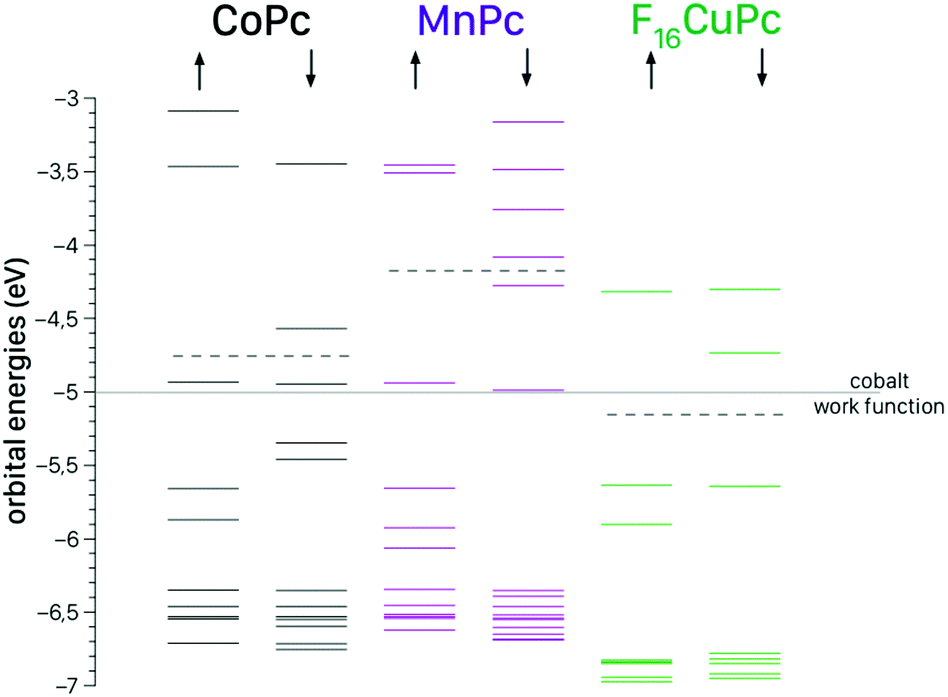 | ||
| Fig. 7 Ground state electronic structures of the metal phthalocyanine molecules as obtained from the DFT calculations. The dotted lines mark the Fermi levels of the individual molecules. | ||
One important parameter that influences transport in the metal phthalocyanine layers is the magnitude of the electronic coupling between the individual molecules. It can be described by means of the so called transfer integral. The value of the transfer integral is proportional to the electronic coupling between molecular building blocks and is also proportional to electron and hole mobilities. With these simple arguments we ignore the impact of electron–phonon interaction. The electron–phonon interaction generally lowers the mobility and depends on the vibrations of the system. Due to the fact that the different phthalocyanines show very similar vibrational spectra we expect very similar impact of the electron–phonon coupling on the mobility.
In Table 1 we show values for the transfer integral t estimated with the energy split method based on calculations on dimer model systems (see Fig. 8). From the values in Table 1, it becomes clear that the electronic coupling is weakest in MnPc. Pure F16CuPc shows an approximately six times higher coupling for te and two times higher values for th compared to pure MnPc. The coupling is also significantly higher than in F16CoPc. For the mixed F16CuPc/MnPc system we obtained the highest values for te and th. The values for F16CoPc/MnPc are somewhat lower than for F16CuPc/MnPc but also clearly above the pure components. The details of the hybrid orbitals are shown in Fig. 8. It is possible to observe that the frontier orbitals of the mixed dimer are formed by hybridization between the MnPc HOMO and the F16CuPc LUMO orbitals. Hence the HOMO (and LUMO) of the mixed dimer is delocalized over both molecular subunits which results in a larger transfer integral and therefore in higher conductivity. It is, however, interesting to note that the overall charge transfer of 0.05 electrons from MnPc to F16CuPc is about a factor of four smaller compared to the 0.20 electrons in the F16CoPc/MnPc dimer.20
 | ||
| Fig. 8 Electronic structure and charge density difference of the dimer model systems (a) MnPc/F16CuPc and (b) MnPc/F16CoPc. | ||
| Material | t e (meV) | t h (meV) | Δρ (electrons) |
|---|---|---|---|
| MnPc | 35 | 45 | — |
| F16CuPc | 237 | 70 | — |
| F16CoPc | 108 | 53 | — |
| F16CuPc/MnPc | 192 | 252 | 0.05 |
| F16CoPc/MnPc | 79 | 126 | 0.20 |
An interesting observation is the correlation between electronic coupling and conductivity on the one hand (Fig. 6a), and between magnitudes of the charge transfer in the mixed systems and rectification ratio on the other hand (Fig. 6b). The experimental results presented in Fig. 6 show that the systems with the higher electronic coupling show the higher conductivity. The F16CoPc/MnPc system shows higher rectification ratio than F16CuPc/MnPc. The charge transfer at the F16CoPc/MnPc interface results in the formation of an internal electric field and acts therefore like an intrinsic pn-junction. These findings may indicate that the magnitude of the charge transfer is directly related to the achieved rectification ratio.
3. Methods and theory details
3.1 Metal-phthalocyanine films and back bottom electrode
A 20 nm thick Co film works as a back bottom electrode. This back electrode is deposited on top of a 1 μm thick thermally grown SiO2 on a Si (100) wafer. The thick SiO2 provides a reliable electrical isolation of the Co electrode from the back substrate and minimizes leakage currents. The Co electrode is deposited via sputtering with a rate of 0.04 nm s−1 at a vacuum of about 5 × 10⁻³ mbar. Metal-phthalocyanine films were deposited via organic molecular beam deposition (OMBD). All organic films studied here are prepared under similar conditions, including evaporation rates of 0.01 nm s−1, vacuum of about 5 × 10⁻⁷ mbar and temperatures of about 300 °C and 340 °C, for the MnPc and fluorinated phthalocyanine films, respectively. Both, the Co back bottom electrode and the organic thin films are deposited in situ, without breaking vacuum conditions in order to ensure an oxide-free metal–organic interface (customized Moorfield MiniLab 060 system).3.2 Nanoscale electrical measurements via current sensing atomic force microscopy (cs-AFM)
Electrical measurements are performed via cs-AFM modes (Keysight Technologies, 5500 AFM), including local I–V spectroscopy and dynamic current mapping. Topography and current data are recorded simultaneously, in contact mode, using Pt-coated Si cantilevers with a typical spring constant of 0.2 N m−1 and average radius dimensions of <25 nm.49 The voltage is applied directly to the Co back electrode, while the grounded conductive cantilever is used as a top electrode (see Fig. 1a). An environment protection closed chamber is purged several times with nitrogen and argon gas flow before the AFM experiments. All AFM measurements are performed under a well-controlled argon atmosphere (a controlled flow of argon is kept constant during all the AFM based electrical measurements) in order to preserve the integrity of the organic films and to avoid possible influence of the environment on the transport properties of the material. AFM probe deflection is monitored during all electrical measurements in order to ensure that the feedback system maintains a constant contact force, and force–distance curves are measured to verify the quality of the probe which may affect the measurement of the electric current (see ESI S2†). AFM topography and current mapping images are analyzed using WSxM50 and Gwyddion51 software.3.3 DFT calculations
The unrestricted density functional theory (DFT) calculations within this work are carried out using the GPAW program package.52 If not stated otherwise all calculations are performed at the GGA/PBE level of theory using a local orbital double-zeta polarized basis set.53 We also include semi-empirical dispersion correction at the DFT-D3 level according to Grimme et al.54For the model dimer systems, the geometries used are built based on the thermodynamically stable beta-phase. As starting point we place the molecular planes 3.1 Å apart from each other. The central metal atom of the respective phthalocyanine is placed below (above) the nitrogen atom that bridges the isoindolic units in the molecule. A subsequent geometry optimization of the dimer models is performed to obtain interatomic forces below 0.01 eV Å−1. During this relaxation the initial distance of the molecular planes typically shortens between 0.1 and 0.2 Å.
Based on the electronic structure of the dimer model systems we estimate fundamental electronic coupling parameters. The transfer integral t for neighboring molecules is a direct measure for possible maximum values of electron and hole mobility in a material.55 We calculate values for t based on dimer models by using the energy split method, which is approximated as th = (ε[H] − ε[H−1])/2 and te = (ε[L−1] − εL)/2, where ε[L,H] and ε[L+1,H−1] are the orbital energies of the LUMO, LUMO+1 and HOMO, HOMO−1 levels of a neutral dimer.
4. Conclusions
We report on the transport properties of phthalocyanine based heterostructures and the well-controlled enhancement of its charge transfer capabilities by the tuning of its structural configuration. By employing conductive atomic force microscopy techniques, we provide an insight about the nanoscale transport mechanisms of MnPc and fluorinated phthalocyanines such as F16CuPc and F16CoPc. A transition from typical diode-like transport mechanisms to space-charge-limited current transport regime (SCLC) is observed from pure MnPc thin films to the Pc-based heterostructures. Taking advantage of the AFM techniques implemented here, we present a method to spatially map the mobility of the F16CuPc/MnPc structures with a nanoscale resolution. To support our experimental findings, we also provide theoretical DFT calculations which indicated higher values of the te and th transfer integrals (therefore higher conductivity) for the case of the F16CuPc/MnPc heterostructure system, due to the fact that the orbitals of the mixed dimer are formed by hybridization between the MnPc HOMO and the F16CuPc LUMO orbitals. Hence the HOMO (and LUMO) of the mixed dimer is delocalized over both molecular subunits. This well-controlled nanoscale tuning of the electrical properties for metal transition phthalocyanine junctions stands as key step for future phthalocyanine-based electronic devices, where the low dimension charge transfer, mediated by transition metal atoms could be intrinsically linked to a transfer of magnetic moment or spin.Acknowledgements
The authors acknowledge financial support by the Deutsche Forschungsgemeinschaft DFG FOR 1154 “Towards Molecular Spintronics”.Notes and references
- R. S. Potember, T. O. Poehler and D. O. Cowan, Appl. Phys. Lett., 1979, 34, 405 CrossRef CAS.
- T. Reda, A. F. Collings, C. Barton and P. Lukins, J. Phys. Chem. B, 2003, 107, 13774–13781 CrossRef CAS.
- B. Koo, H. Baek and J. Cho, Chem. Mater., 2012, 24, 1091–1099 CrossRef CAS.
- K. V. Raman, A. M. Kamerbeek, A. Mukherjee, N. Atodiresei, T. K. Sen, P. Lazić, V. Caciuc, R. Michel, D. Stalke, S. K. Mandal, S. Blügel, M. Münzenberg and J. S. Moodera, Nature, 2013, 493, 509–513 CrossRef CAS PubMed.
- Y. Morita, S. Nishida, T. Murata, M. Moriguchi, A. Ueda, M. Satoh, K. Arifuku, K. Sato and T. Takui, Nat. Mater., 2011, 10, 947–951 CrossRef CAS PubMed.
- J. M. Manriquez, G. T. Yee, R. S. Mclean, A. J. Epstein and J. S. Miller, Science, 1991, 252, 1415–1417 CAS.
- C. Herrmann, G. C. Solomon and M. A. Ratner, J. Am. Chem. Soc., 2010, 132, 3682–3684 CrossRef CAS PubMed.
- K. Yoshida, I. Hamada, S. Sakata, A. Umeno, M. Tsukada and K. Hirakawa, Nano Lett., 2013, 13, 481–485 CrossRef CAS PubMed.
- J. Wang, H. Wang, X. Yan, H. Huang and D. Yan, Appl. Phys. Lett., 2005, 87, 093507 CrossRef.
- H. Wang, J. Wang, H. Huang, X. Yan and D. Yan, Org. Electron., 2006, 7, 369–374 CrossRef CAS.
- H. Wang and D. Yan, NPG Asia Mater., 2010, 2, 69–78 CrossRef.
- H. Alves, A. S. Molinari, H. Xie and A. F. Morpurgo, Nat. Mater., 2008, 7, 574–580 CrossRef CAS PubMed.
- S. Wen, W.-Q. Deng and K.-L. Han, Chem. Commun., 2010, 46, 5133 RSC.
- I. G. Lezama, M. Nakano, N. A. Minder, Z. Chen, F. V. Di Girolamo, A. Facchetti and A. F. Morpurgo, Nat. Mater., 2012, 11, 788–794 CrossRef CAS PubMed.
- C. W. Chu, J. M. E. Harper, T. H. Geballe and R. L. Greene, Phys. Rev. Lett., 1973, 31, 1491–1494 CrossRef CAS.
- L. B. Coleman, M. J. Cohen, D. J. Sandman, F. G. Yamagishi, A. F. Garito and A. J. Heeger, Solid State Commun., 1973, 12, 1125–1132 CrossRef CAS.
- H. Seo, C. Hotta and H. Fukuyama, Chem. Rev., 2004, 104, 5005–5036 CrossRef CAS PubMed.
- K. Walzer, B. Maennig, M. Pfeiffer and K. Leo, Chem. Rev., 2007, 107, 1233–1271 CrossRef CAS PubMed.
- N. Koch, S. Duhm, J. P. Rabe, A. Vollmer and R. L. Johnson, Phys. Rev. Lett., 2005, 95, 237601 CrossRef PubMed.
- S. Lindner, M. Knupfer, R. Friedrich, T. Hahn and J. Kortus, Phys. Rev. Lett., 2012, 109, 027601 CrossRef PubMed.
- S. Lindner, B. Mahns, U. Treske, O. Vilkov, F. Haidu, M. Fronk, D. R. T. Zahn and M. Knupfer, J. Chem. Phys., 2014, 141, 094706 CrossRef PubMed.
- S. Lindner, B. Mahns, A. König, F. Roth, M. Knupfer, R. Friedrich, T. Hahn and J. Kortus, J. Chem. Phys., 2013, 138, 024707 CrossRef PubMed.
- N. R. Armstrong, P. A. Veneman, E. Ratcliff, D. Placencia and M. Brumbach, Acc. Chem. Res., 2009, 42, 1748–1757 CrossRef CAS PubMed.
- O. G. Reid, K. Munechika and D. S. Ginger, Nano Lett., 2008, 8, 1602–1609 CrossRef CAS PubMed.
- H.-N. Lin, S.-H. Chen, G.-Y. Perng and S.-A. Chen, J. Appl. Phys., 2001, 89, 3976 CrossRef CAS.
- A. Alexeev, J. Loos and M. M. Koetse, Ultramicroscopy, 2006, 106, 191–199 CrossRef CAS PubMed.
- G. A. MacDonald, P. A. Veneman, D. Placencia and N. R. Armstrong, ACS Nano, 2012, 6, 9623–9636 CrossRef CAS PubMed.
- P. F. Siles, C. C. B. Bufon, D. Grimm, A. R. Jalil, C. Mende, F. Lungwitz, G. Salvan, D. R. T. Zahn, H. Lang and O. G. Schmidt, Org. Electron., 2014, 15, 1432–1439 CrossRef CAS.
- P. Robaschik, P. F. Siles, D. Bülz, P. Richter, M. Monecke, M. Fronk, S. Klyatskaya, D. Grimm, O. G. Schmidt, M. Ruben, D. R. T. Zahn and G. Salvan, Beilstein J. Nanotechnol., 2014, 5, 2070–2078 CrossRef PubMed.
- M. C. Schalnat, A. M. Hawkridge and J. E. Pemberton, J. Phys. Chem. C, 2011, 115, 13717–13724 CAS.
- M. Serri, W. Wu, L. R. Fleet, N. M. Harrison, C. F. Hirjibehedin, C. W. M. Kay, A. J. Fisher, G. Aeppli and S. Heutz, Nat. Commun., 2014, 5 Search PubMed.
- K. J. Franke, G. Schulze and J. I. Pascual, Science, 2011, 332, 940–944 CrossRef CAS PubMed.
- T. L. Anderson, G. C. Komplin and W. J. Pietro, J. Phys. Chem., 1993, 97, 6577–6578 CrossRef CAS.
- A. K. Ghosh, D. L. Morel, T. Feng, R. F. Shaw and C. A. Rowe, J. Appl. Phys., 1974, 45, 230 CrossRef CAS.
- W. J. Pietro, Adv. Mater., 1994, 6, 239–242 CrossRef CAS.
- G. Horowitz, D. Fichou, X. Peng and P. Delannoy, J. Phys., 1990, 51, 1489–1499 CAS.
- R. D. Gould, Coord. Chem. Rev., 1996, 156, 237–274 CrossRef CAS.
- S. Samanta, D. K. Aswal, A. Singh, A. K. Debnath, M. S. Kumar, Y. Hayakawa, S. K. Gupta and J. V. Yakhmi, Appl. Phys. Lett., 2010, 96, 013305 CrossRef.
- A. K. Debnath, A. Kumar, S. Samanta, R. Prasad, A. Singh, A. K. Chauhan, P. Veerender, S. Singh, S. Basu, D. K. Aswal and S. K. Gupta, Appl. Phys. Lett., 2012, 100, 142104 CrossRef.
- K. R. Rajesh and C. S. Menon, Eur. Phys. J. B, 2005, 47, 171–176 CrossRef CAS.
- C. C. Bof Bufon, C. Vervacke, D. J. Thurmer, M. Fronk, G. Salvan, S. Lindner, M. Knupfer, D. R. T. Zahn and O. G. Schmidt, J. Phys. Chem. C, 2014, 118, 7272–7279 CAS.
- N. B. McKeown, Phthalocyanine materials: synthesis, structure, and function, Cambridge University Press, Cambridge, U.K., New York, 1998 Search PubMed.
- H. Peisert, T. Schwieger, J. M. Auerhammer, M. Knupfer, M. S. Golden, J. Fink, P. R. Bressler and M. Mast, J. Appl. Phys., 2001, 90, 466 CrossRef CAS.
- D. Qi, J. Sun, X. Gao, L. Wang, S. Chen, K. P. Loh and A. T. S. Wee, Langmuir, 2010, 26, 165–172 CrossRef CAS PubMed.
- W. Chen, D.-C. Qi, H. Huang, X. Gao and A. T. S. Wee, Adv. Funct. Mater., 2011, 21, 410–424 CrossRef CAS.
- D. G. de Oteyza, A. El-Sayed, J. M. Garcia-Lastra, E. Goiri, T. N. Krauss, A. Turak, E. Barrena, H. Dosch, J. Zegenhagen, A. Rubio, Y. Wakayama and J. E. Ortega, J. Chem. Phys., 2010, 133, 214703 CrossRef CAS PubMed.
- F. Zhu, J. Yang, D. Song, C. Li and D. Yan, Appl. Phys. Lett., 2009, 94, 143305 CrossRef.
- Y. Zhang, H. Dong, Q. Tang, S. Ferdous, F. Liu, S. C. B. Mannsfeld, W. Hu and A. L. Briseno, J. Am. Chem. Soc., 2010, 132, 11580–11584 CrossRef CAS PubMed.
- See http://www.nanoandmore.com/AFM-Probe-ElectriCont-G.html, 2015.
- I. Horcas, R. Fernández, J. M. Gómez-Rodríguez, J. Colchero, J. Gómez-Herrero and A. M. Baro, Rev. Sci. Instrum., 2007, 78, 013705 CrossRef CAS PubMed.
- See Gwyddion free SPM multimodular software, http://gwyddion.net/, 2015.
- J. Enkovaara, C. Rostgaard, J. J. Mortensen, J. Chen, M. Dułak, L. Ferrighi, J. Gavnholt, C. Glinsvad, V. Haikola, H. A. Hansen, H. H. Kristoffersen, M. Kuisma, A. H. Larsen, L. Lehtovaara, M. Ljungberg, O. Lopez-Acevedo, P. G. Moses, J. Ojanen, T. Olsen, V. Petzold, N. A. Romero, J. Stausholm-Møller, M. Strange, G. A. Tritsaris, M. Vanin, M. Walter, B. Hammer, H. Häkkinen, G. K. H. Madsen, R. M. Nieminen, J. K. Nørskov, M. Puska, T. T. Rantala, J. Schiøtz, K. S. Thygesen and K. W. Jacobsen, J. Phys.: Condens. Matter, 2010, 22, 253202 CrossRef CAS PubMed.
- J. M. Soler, E. Artacho, J. D. Gale, A. García, J. Junquera, P. Ordejón and D. Sánchez-Portal, J. Phys.: Condens. Matter, 2002, 14, 2745–2779 CrossRef CAS.
- S. Grimme, J. Antony, S. Ehrlich and H. Krieg, J. Chem. Phys., 2010, 132, 154104 CrossRef PubMed.
- V. Coropceanu, J. Cornil, D. A. da Silva Filho, Y. Olivier, R. Silbey and J.-L. Brédas, Chem. Rev., 2007, 107, 926–952 CrossRef CAS PubMed.
Footnote |
| † Electronic supplementary information (ESI) available. See DOI: 10.1039/c5nr08671j |
| This journal is © The Royal Society of Chemistry 2016 |