
 Open Access Article
 This Open Access Article is licensed under a
 Creative Commons Attribution 3.0 Unported Licence
Tuning the surface electronic structure of a Pt3Ti(111) electro catalyst†
M.
Paßens
a,
V.
Caciuc
b,
N.
Atodiresei
*b,
M.
Moors
a,
S.
Blügel
b,
R.
Waser
ac and
S.
Karthäuser
*a
aPeter Grünberg Institut (PGI-7) and JARA-FIT, Forschungszentrum Jülich GmbH, 52425 Jülich, Germany. E-mail: s.karthaeuser@fz-juelich.de
bPeter Grünberg Institut (PGI-1) and Institute for Advanced Simulation (IAS-1), Forschungszentrum Jülich GmbH, 52425 Jülich, Germany
cIWE2 and JARA-FIT, RWTH Aachen University, 52056 Aachen, Germany
First published on 25th January 2016
Abstract
Increasing the efficiency and stability of bimetallic electro catalysts is particularly important for future clean energy technologies. However, the relationship between the surface termination of these alloys and their catalytic activity is poorly understood. Therefore, we report on fundamental UHV-SPM, LEED, and DFT calculations of the Pt3Ti(111) single crystal surface. Using voltage dependent imaging the surface termination of Pt3Ti(111) was studied with atomic resolution. Combining these images with simulated STM maps based on ab initio DFT calculations allowed us to identify the three upper layers of the Pt3Ti(111) single crystal and their influence upon the surface electronic structure. Our results show that small changes in the composition of the second and third atomic layer are of significant influence upon the surface electronic structure of the Pt3Ti electro catalyst. Furthermore, we provide relevant insights into the dependence of the surface termination on the preparation conditions.
Introduction
The development of clean energy production and storage methods is one of the most important issues of current scientific investigations. Among others, hydrogen based energy systems, like proton exchange membrane fuel cells, seem to be a promising approach for future applications. At present however, there is a great need for improved Pt-based cathode catalysts for the oxygen reduction reaction (ORR), so that the Pt loading can be reduced.1 A well-known option to develop high efficient electro catalysts is alloying two or more metals. This often leads to newly arising surface phenomena, which are important for their catalytic properties.In this connection employing Pt-alloys with 3d and 4d-transition metals (Pt3M with M = Ni, Co, Fe, Ti, V, Y, Zr) leads to ‘volcano-type’ electro catalytic trends.2–4 The maximum in the catalytic activity in Pt3M alloys is due to the interplay between the adsorption of reactive intermediates and the efficiency of the electron transfer to adsorbates. That is, if cathode catalysts bind O2 too strongly the ORR rate is limited by the desorption rate of the reduced species, otherwise the ORR rate is limited by the electron transfer rate to the oxygen species.
In the series of Pt3M alloys the ‘volcano-type’ trend in the catalytic activity of the ORR across the periodic table can be correlated to the surface electronic structure.2–4 Since the metal–adsorbate interaction depends on the coupling between the oxygen 2p-states and the metal d-states, the d-band center corresponds in the same way as the chemisorption energy to the kinetic of the ORR and thus, can be used as measure for the electro catalytic activity of the respective Pt-alloy. Consequently, the rules for the development of efficient electro catalysts, based on experimental and calculated data given in literature2–5 seem to be clear. The d-band center of an ideal electro catalyst should be shifted −0.2 eV relative to the one of Pt and the catalyst should bind oxygen about 0.2 eV weaker than Pt does it.
However, while the influence of the 3d and 4d-transition metals on the ORR rate is obvious, the production of an ideal electro catalyst is experimentally complex. One issue is the enhanced dissolution of the transition metal in aqueous solutions with respect to Pt which can cause an increase of Pt in the surface region.6 Another aspect are surface segregation effects depending on the exact stoichiometry of the alloys. These segregation effects turn out to be an important source for changes in the surface electronic structure of Pt3M alloys.2,5 It could be shown experimentally and theoretically that the bulk-like termination consisting of 75% Pt and 25% M atoms and the Pt-skin termination, that is a pure Pt outermost layer covering a bulk Pt3M alloy, differ considerably in ORR rate, chemisorption energy and d-band center. Moreover, it was theoretically predicted that a strong segregation of Pt to the outermost layer will occur in alloys, especially Pt3Ti, whose Pt concentration is above 75%.5 Indeed currently, it is largely believed, mainly based on low-energy ion-scattering spectroscopy (LEIS) and tensor low-energy electron diffraction (LEED) measurements, that after the usual preparing conditions of Pt3M-crystals (sputtering/annealing cycles in ultrahigh-vacuum (UHV)) a Pt-skin covers the atomic layers underneath and in addition, acts as protective layer.2–4,7,8 This is especially of importance with respect to a high corrosion resistance of the alloy. The challenge is to prepare a Pt3M alloy and tune the surface segregation process in such a way that the above mentioned properties of an ideal electro catalyst are achieved. So far however, contradictory assumptions about the surface segregation process exist, e.g. it is not clear whether the Pt3M-layer beneath the Pt-skin is Pt-depleted or not.4,5,9–11 Since the binding energies of adsorbates on the alloy surface show a strong sublayer dependence,10,12 the task to develop an improved electro catalyst is demanding and theoretical predictions are difficult.
Due to the fact that there is a great need for the identification of the fundamental segregation mechanisms at the surface we use a well-characterized single crystal material and examine the surface properties at the nanoscale. In detail, we focus on Pt3Ti, a stoichiometric intermetallic phase, which crystallizes in the Cu3Au-type with a cubic face centered structure and a lattice constant of 0.3906 nm, which is only 0.4% smaller than the value for pure platinum.8 This results in an interatomic distance of 0.276 nm on the hexagonal (111) orientated surface. LEED studies indicate a titanium induced p(2 × 2) superstructure with respect to the p(1 × 1) spots of a pure Pt(111) crystal.7,13,14 On the other hand, one real space study of the surface morphology using scanning tunneling microscopy (STM) could verify the p(2 × 2) but not the p(1 × 1) structure.8
The high stability of the Pt3Ti crystal structure, indicated by its high melting point of 2213 K, is caused by a strong interaction of the Pt 5d and the Ti 3d bands in the bulk and makes it interesting for catalytic applications.14–16 In addition, recent DFT calculations indicate a significant lowering of the activation energy for the rate determining step in the ORR compared to the Pt(111) surface.1,17 Furthermore, due to its highly defined surface structure the Pt3Ti-surface is even suitable for the controlled growth of thin titanium oxide films, which stand out by their high degree of surface order and reproducibility.18 The surface oxidation process is accomplished by the diffusion of Ti from the bulk to the surface at elevated temperatures. Depending on the growth conditions several different oxide phases can be formed, which differ in their stoichiometry, symmetry and thickness.11
These results offer a wide range of possible applications of Pt3Ti and oxidized Pt3Ti surfaces as tunable electro catalysts once the surface segregation mechanism is fully understood. Therefore, we apply here a methodologically sound approach which is suitable to reveal surface transformations in the sub-nanometer range. We will evidence the true nature of the clean Pt3Ti(111) single crystal surface by combining UHV-SPM methods, especially voltage-dependent imaging, which will allow us to characterize the surface layer of the electro catalyst with atomic resolution, with simulated STM maps based on ab initio DFT calculations assuming different crystal terminations. This combination will allow us to identify the outermost surface layer and the layers underneath together with their influence upon the surface electronic structure.
Methods
Sample preparation
A Pt3Ti(111) single crystal was purchased from MaTecK and has been prepared by several sputtering/annealing cycles under UHV conditions. Sputtering was performed with an IQE 11 ion gun (Specs, Germany) operating at 1 keV for 10 minutes under normal incidence with a neon pressure of 1 × 10⁻⁵ mbar (1 μA sample current) for sample 1 (S1) and with 3 × 10⁻⁵ mbar neon pressure (3 μA sample current) for sample 2 (S2). In order to heal out the crystal surface the sample has been annealed to 1200 K for 25 minutes after each sputter cycle. The cleanliness of the surface has been checked by LEED and STM.STM measurements
All experiments were carried out in a Createc low temperature STM, which was operated at a working pressure of 1 × 10⁻¹⁰ mbar. The UHV system consists of a stainless steel vessel and is additionally equipped with a combined MCP-LEED/Auger spectrometer, a sputter gun for surface preparation and a mass spectrometer for rest gas analysis. All UHV-STM and STS measurements were performed in constant current mode at liquid nitrogen temperature using electrochemically etched tungsten tips. Some measurements were performed in the so called multiple voltage mode. In this mode images are taken parallel line by line, each line with a different bias voltage applied, so that a series of images is measured in one scan. The dI/dV spectra were measured with lock-in technique, using a small ac modulation voltage (amplitude = 40 mV, frequency = 476 Hz) added to the sample bias, while the feedback loop was deactivated. All spectroscopy data shown here are averaged over 4 to 20 individual curves recorded within 15 seconds (see text).LEED measurements
The LEED images were taken with an OCI BDL800IR-MCP LEED system using a filament current of 2.55 A and a screen voltage of 3 keV. Due to the use of two microchannel plates the electron beam current never exceeded a value of 200 nA, so that a beam induced surface damage can be excluded.DFT calculations
Our density functional theory (DFT)19 simulations were performed using the all-electron frozen core projector augmented wave method20 as implemented in the VASP code.21,22 The clean Pt3Ti(111) geometry was modeled by a slab consisting of 5 atomic layers using the theoretical lattice parameter of 3.949 Å, while the one and two Pt overlayers on Pt3Ti(111) were obtained by replacing the surface atoms with Pt ones. In all our supercells calculations, i.e., for the bulk terminated Pt3Ti(111), one and two Pt overlayers on Pt3Ti(111), and one Ti overlayer on Pt3Ti(111), we always relaxed three surface layers while two atomic Pt3Ti layers were kept fixed. Additionally, our first-principles calculations employed the Perdew–Burke–Ernzerhof exchange correlation functional,23 an energy cut-off energy of 500 eV, a Brillouin zone sampling by a mesh of 8 × 8 × 1, and the relaxed geometries were obtained when the calculated Hellmann–Feynman forces acting on the two surface layers were less than 1 meV Å−1.Results and discussion
Surface termination of Pt3Ti(111)
As a typical representative of a binary metal alloy with Cu3Au structure the unreconstructed hexagonal Pt3Ti(111) surface should be build up by ABCABC… stacked layers, all consisting of three Pt atoms and one Ti atom per unit cell. In this case the Ti atoms form a p(2 × 2) superlattice with respect to the p(1 × 1) lattice of a pure Pt(111) surface. The LEED pattern was taken of the clean Pt3Ti(111) single crystal surface at 180 eV beam energy after an extensive surface preparation using Ne gas sputtering and subsequent annealing cycles (see Fig. S1 in ESI†). The expected spots of a p(2 × 2) superstructure can be clearly detected and the determined unit cell vectors are 0.554 nm and 0.276 nm (see Fig. S1b†) due to the nearly identical atom radii of Pt and Ti. Therefore, the LEED image is in accordance with a bulk-like surface with a Ti related p(2 × 2) superlattice and a Pt related p(1 × 1) sub unit cell (see Fig. S1c†).However, it is known that LEED has only a limited surface sensitivity. The penetration depth of scattered electrons with kinetic energies between 100 and 200 eV, which is a typical range for LEED measurements, is in the order of 0.5–1 nm.24 Consequently, the LEED image indicates that the Pt3Ti(111) single crystal surface is well-ordered in the surface region, but cannot provide distinct information about the topmost surface layer.
Since scanning probe methods are surface sensitive in the sub nanometer range and reveal both, morphological changes and variations in the electronic surface structure, we apply this method to get further insights into the Pt3Ti(111) single crystal surface. Fig. 1(a) shows the UHV-STM image of the Pt3Ti(111) surface with one atomic step and a screw dislocation, which is also characteristic for Pt(111) surfaces. The step height was estimated to be around 0.23 nm and is in accordance with crystallographic data. Furthermore, very small adsorbates, presumably hydrogen which cannot be removed completely from the UHV-system, and even smaller surface defects are visible. A close-up view of the Pt3Ti(111) surface is given in Fig. 1(b). It reveals clearly the hexagonal symmetry and the unit cell of the Ti related p(2 × 2) superstructure with a cell constant of 0.56 nm. In addition, one defect can easily be identified by the changed contrast in the middle of the STM image, which will be discussed later in detail.
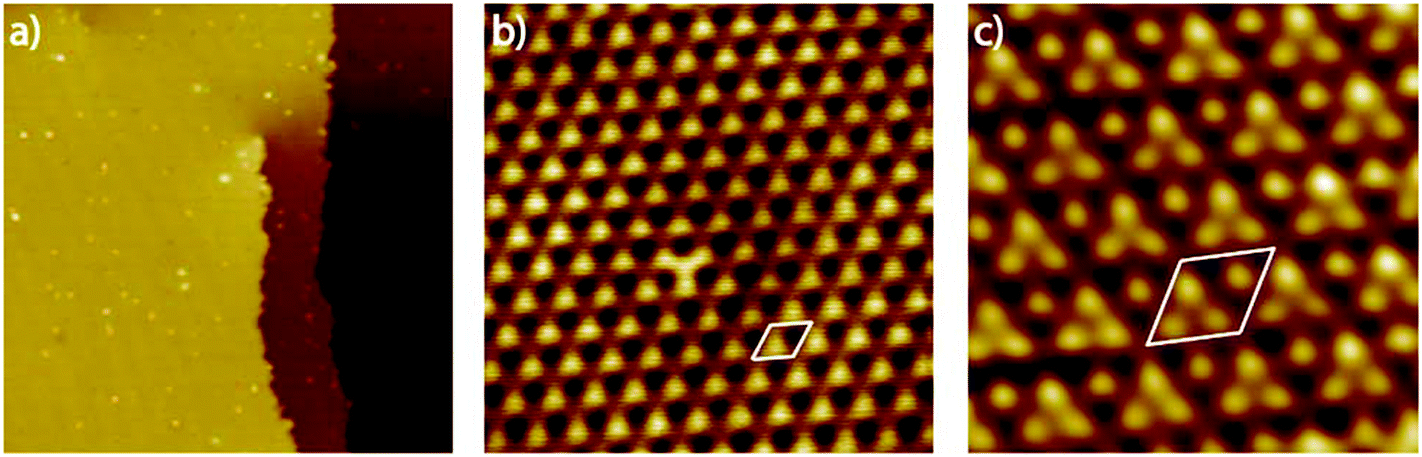 | ||
| Fig. 1 (a) UHV-STM image of the Pt3Ti surface with one atomic step and a screw dislocation (sample 1 = S1). Furthermore, some surface defects and adsorbates are visible (57.5 nm × 57.5 nm, 2.31 V; 0.01 nA). (b) High-resolution image with one surface defect. The Ti induced p(2 × 2) superstructure is clearly visible (S1, 6.25 nm × 6.25 nm, 1.3 V, 0.11 nA); (c) UHV-STM of the Pt3Ti surface after repeated cleaning cycles with atomic resolution (S2, 2.50 nm × 2.50 nm, 0.006 V, 7.9 nA, (low pass filtered)). | ||
So far, the UHV-STM investigations of the Pt3Ti(111) surface exhibit the periodicity of the bulk crystal. However, since STM images are a convolution of the surface morphology and the electronic structure this does not necessarily indicate a bulk-like termination of the Pt3Ti single crystal. Moreover, the pronounced sublayer dependence of the binding energies of adsorbates should be taken into account.10,12 This means that the d-band center and also the electronic structure of the surface, which is probed here, depends at least on the topmost and the second surface layer.
In order to achieve an even higher resolution of the Pt3Ti(111) surface we varied the STM parameters and the preparation conditions of the single crystal surface. Finally, as a result of intense optimization we obtained the UHV-STM image shown in Fig. 1(c). The atomic resolution of this image of the Pt3Ti single crystal surface reveals three positions with equivalent electron density forming a triangle and one position which seems to be isolated. The key question is: Does this UHV-STM image with atomic resolution show the bulk-like termination of the Pt3Ti single crystal? On one hand the 3![[thin space (1/6-em)]](https://www.rsc.org/images/entities/char_2009.gif) :1 relation of atomic identities and the surface symmetry points to a bulk-like termination. On the other hand, the apparent height differences in Fig. 1(c) amount at most to 40–50 pm, which is in the size-range of surface corrugation effects. Moreover, a Pt-skin surface, like introduced above, would also show the same symmetry resulting from the surface electronic structure due to the underlying bulk structure.
:1 relation of atomic identities and the surface symmetry points to a bulk-like termination. On the other hand, the apparent height differences in Fig. 1(c) amount at most to 40–50 pm, which is in the size-range of surface corrugation effects. Moreover, a Pt-skin surface, like introduced above, would also show the same symmetry resulting from the surface electronic structure due to the underlying bulk structure.
To complicate the situation even more, we noticed that the appearance of the Pt3Ti single crystal surface depends strongly on the used bias voltage (Vbias) during the STM measurements and in addition on the preparation conditions, i.e. the cleaning/annealing cycles of the sample. At this point a thorough systematic investigation was started. We prepared the Pt3Ti single crystal in two distinct ways, i.e. method 1 (S1) with a soft Ne+-sputtering at 1 × 10⁻⁵ mbar and method 2 (S2) with a more intense sputtering at 3 × 10⁻⁵ mbar, respectively, using the same sputtering time and acceleration voltage. The annealing step was kept constant. The differently prepared Pt3Ti single crystal surfaces, S1 and S2, were characterized with STM using the same series of Vbias settings in two different modes. In one mode we collected the whole series of STM images at different Vbias in one scan (multiple voltages mode). This series is useful to determine the lateral shift of appearing features in the STM image. From Fig. S2 in ESI† it can be deduced, that indeed a lateral shift of the dominant features appears in S1 between 0.58 V and 1.3 V, while for S2 the shift takes place between 1.3 V and 1.96 V. Subsequently, the Pt3Ti surface structure was characterized with high resolution at the same Vbias settings. Cutouts of the obtained STM images at selected Vbias for both samples, S1 and S2, respectively, are displayed in Fig. 2. Only Vbias values in the positive voltage range, imaging unoccupied electronic states of the Pt3Ti surface, have been selected, since the thus obtained STM images are the most characteristic ones.
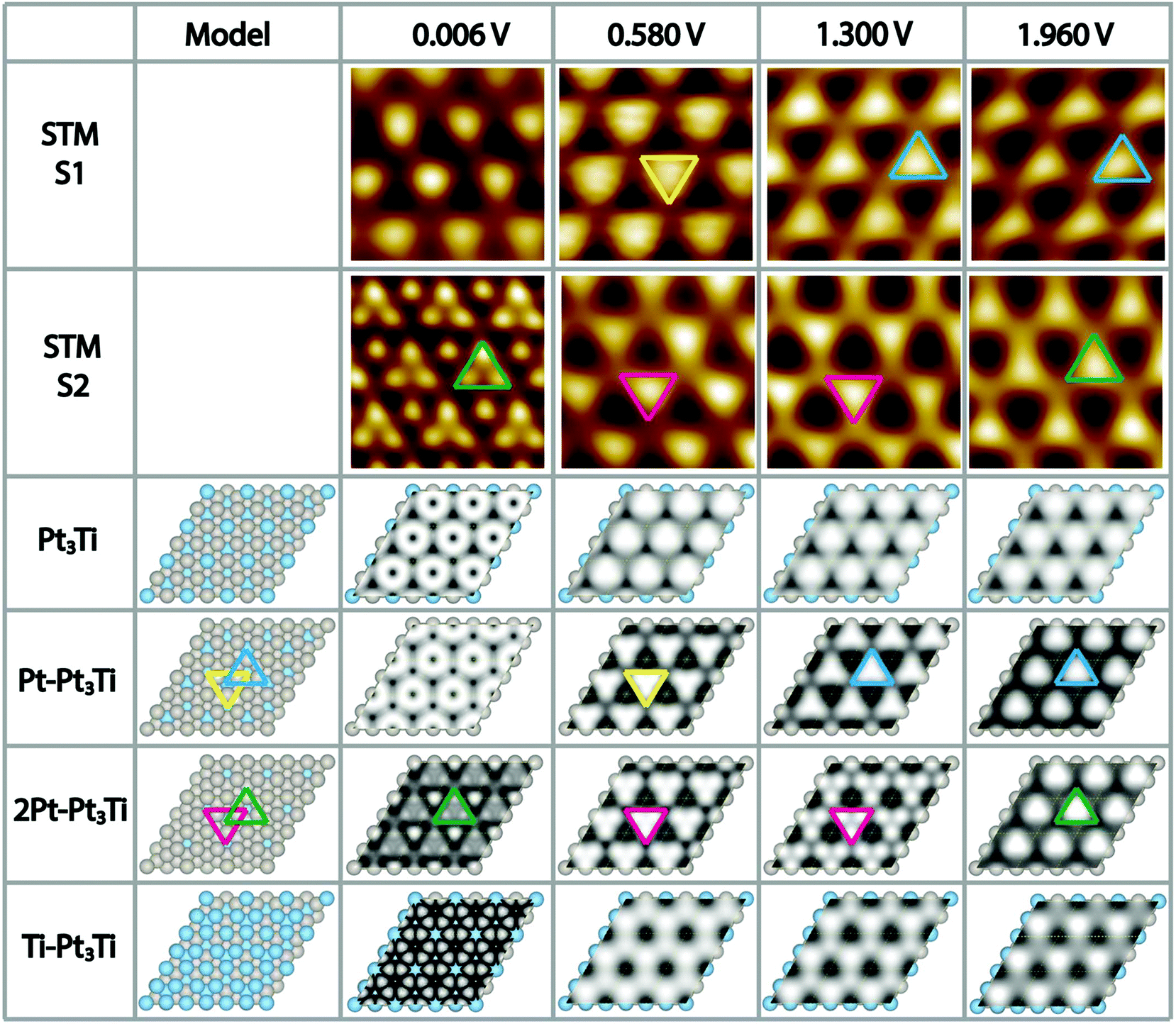 | ||
| Fig. 2 Comparison of high-resolution UHV-STM images (1.5 nm × 1.5 nm, low pass filtered) and ab initio DFT calculations of the Pt3Ti(111) surface. In the first and second row STM images of sample 1 (S1) and sample 2 (S2), prepared under different conditions (see text), are shown for selected sample bias voltages, indicated at the top of each column. The calculated STM images corresponding to the respective bias voltages for four different surface terminations, i.e. bulk termination, Pt layer termination, two layers of Pt termination and Ti layer termination, are shown in row 3 to row 6. For the explanation of the colored triangles see text. | ||
Comparing both series of STM images directly points to the fact that they are characteristic for both samples, S1 and S2, and thus, for the preparation conditions. However, an unambiguous identification of the surface termination is only possible with additional information, like simulated STM maps deduced from ab initio DFT calculations of the Pt3Ti single crystal with different topmost layers.
Regarding the Vbias dependent sequence of the appearance of the Pt3Ti(111) surface of the first sample in more detail (S1, first row in Fig. 2) a distinct change in the features is observed. While for Vbias = 0.006 V slightly indefinite features are received, there are clear triangles with the peak pointing downwards for Vbias = 0.58 V (marked in yellow). However, this appearance changes in a reproducible way when Vbias is raised to 1.3 V. Now the triangles point with their peaks upwards and correspond to other atoms on the Pt3Ti surface. This appearance is preserved also for Vbias = 1.96 V. Comparing this sequence of bias dependent STM images of S1 with the calculated STM images a comprehensive agreement is found with the Pt3Ti crystal surface covered by one monolayer of Pt atoms (Pt–Pt3Ti, row 4 in Fig. 2), which has been proposed to be the surface termination mainly based on LEIS and LEED.2–4,7,8 Especially the flip of the apparent triangle between Vbias = 0.58 V and 1.3 V in orientation and location can be identified in the same way in the simulated STM maps. Moreover, the simulated STM maps allow us to assign the triangles to the corresponding atomic surface structure. While at 0.58 V the apparent triangles correspond to three Pt atoms with direct contact to one Ti atom in the second layer (yellow) the triangles observed at 1.3 V are located above a Ti atom in the third layer (blue). Thus, by applying our method to gather a series of bias dependent STM images and compare them with simulated STM maps based on ab initio DFT calculations, we come to the conclusion that the mildly sputtered Pt3Ti crystal surface (S1) has a Pt–Pt3Ti termination.
Applying the same methodology to the crystal surface S2, which has been sputtered in a more intense way, its surface termination can be identified straightforward. The bias dependent STM images of S2 are given in Fig. 2 row 2. Here, the most striking STM image of the Pt3Ti(111) crystal surface, which shows atomic resolution, was obtained at Vbias = 0.006 V. When using higher bias voltages again triangular features are obtained. However, in this case the orientation and location of the triangle stays constant over the range of 0.58 V < Vbias < 1.3 V (magenta), with only a change in contrast, and flips if Vbias is further increased (green). A comparison of this sequence of bias dependent STM images with the simulated ones points to an all-embracing conformity with a termination of the Pt3Ti single crystal with two Pt layers (2Pt–Pt3Ti, row 5 in Fig. 2). All observations from the experimentally obtained STM images, the atomic resolution at low bias, the triangles with varying contrast at medium bias, and the flip of the triangle in orientation and location at high bias are reflected and can now be used to describe the surface electronic structure at the atomic scale. The triangle built by three Pt atoms of the surface layer located over a Ti atom in the third layer (green) is observed at Vbias = 0.006 V in atomic resolution and at Vbias = 1.96 V. On the other hand the apparent triangle in the range of 0.58 V < Vbias < 1.3 V (magenta) corresponds to three Pt atoms in contact with one Pt atom in the second layer at the center of the triangle. This result indicates that these states are mainly unoccupied states corresponding to the Pt termination. Thus, our results point unambiguously to the fact that sample S2 is formed by two layers of Pt on top of the bulk Pt3Ti single crystal.
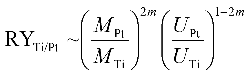
It is worth to note at this point that all STM data have been checked several times on different samples prepared with the “S1 method” and the “S2 method”, respectively, on different places on the sample, and varying the bias voltage back and forth. Thus, clearly the reproducibility of these two surface terminations is proved and their dependence on the here selected preparation conditions. The finding, that soft sputtering at 1 × 10⁻⁵ mbar leads to one monolayer of Pt as surface termination, Pt–Pt3Ti (S1), and more intense sputtering at 3 × 10⁻⁵ mbar to a termination built by two layers of Pt (S2), is a strong evidence that the sputtering procedure has a tremendous influence on the surface termination of bimetallic alloys. Indeed, it is a well-known fact that ion bombardment of alloys can alter the composition of near surface regions, i.e. it can lead to preferential sputtering of one component.25–28 Thus, the component with the lower sputtering yield becomes enriched on the surface. For the pure elements, Pt and Ti, the sputtering yields (atoms/incident ion) are 0.70 and 0.45, respectively, when sputtered with Ne+-ions at 0.6 keV (for sputtering yields with other noble gases see Table S1 in the ESI†).29 This would imply that Ti is enriched in the near surface region. However, there are some alloys, especially those with a large mass difference, that show an enrichment of the heavier component at the surface region.28 Pt with an atomic mass of MPt = 195.0 u is more than four times heavier than Ti with an atomic mass of MTi = 47.8 u. In addition, the surface binding energy of the pure elements is of importance, which is UPt = 5.86 eV and UTi = 4.89 eV.30 The ratio of the yield for two elements (RYTi/Pt), here Pt and Ti, can be expressed by the following formula:
 | (1) |
The term m is proportional to the power cross section used in Sigmund's theory and has a value between 0 and 0.2.28,31 Consequently, the sputtering yield is favored for the element with the lighter mass and the smaller binding energy, which is in both cases true for Ti and should be in the range of 1.2 and 1.5, using the values above. In addition, AES measurements gave values of RYTi/Pt = 1.4 for Ar+-ion bombardment at 0.5 keV and RYTi/Pt = 1.1 for Ar+-ion bombardment at 1.5 keV.32 Therefore, an enrichment of Pt in the surface region due to preferential sputtering is expected. According to the predictions made by Duan et al. this would directly induce surface segregation processes leading to a Pt outermost layer.5 However, what we have identified here is even more sophisticated. The amount of sputtering determines the termination of the Pt3Ti(111) single crystal, i.e. termination by a monolayer of Pt (Pt–Pt3Ti) or by two layers of Pt (2Pt–Pt3Ti).
Surface electronic structure of Pt3Ti(111)
Scanning tunneling spectroscopy (STS) measurements and ab initio PDOS (projected density of states) calculations were performed on Pt3Ti(111) crystal surfaces terminated by a monolayer (S1, Pt–Pt3Ti) or by two layers of Pt (S2, 2Pt–Pt3Ti), respectively. STS measurements taken on Pt–Pt3Ti at three different set points corresponding to three tip-sample distances are presented in Fig. 3(a). A comparison of the resulting STS curves reveals an increase in the background current with an increase of the tunneling voltage for each curve. This increase in the background signal depending on the tunneling voltage and in addition on a reduced tip-sample distance is due to the exponential dependence of the transmission factor on these variables.33 In addition, the absolute values of the peaks in the differential conductance (dI/dV) spectra increase with decreasing tip-sample distance. While the blue curve, corresponding to the largest tip-sample separation, exhibits only small features, the black curve shows distinct peaks, which can be clearly related to surface states.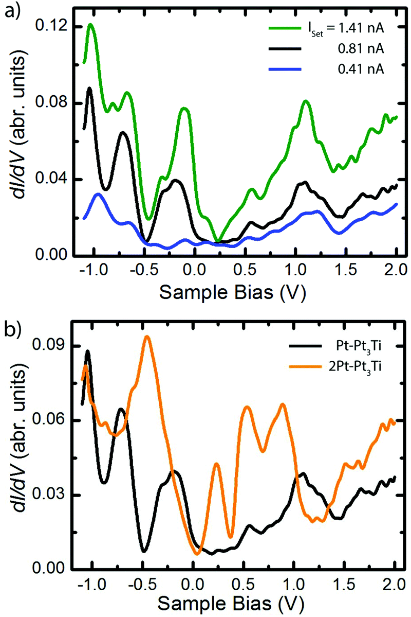 | ||
| Fig. 3 (a) UHV-STS recorded on the Pt–Pt3Ti termination at different heights above the crystal defined by the STS set-point parameters: Vset = −1.10 V, Iset = 0.41 nA, averaged over 10 single curves (blue), Vset = −1.10 V, Iset = 0.81 nA, averaged over 4 single curves (black), Vset = −1.10 V, Iset = 1.41 nA, averaged over 20 single curves (green). (b) Comparison of UHV-STS curves taken from Pt–Pt3Ti (Vset = −1.10 V, Iset = 0.81 nA, averaged over 4 single curves (black)) and 2Pt–Pt3Ti (Vset = −1.00 V, Iset = 0.69 nA, averaged over 10 single curves (orange)), respectively. The resolution of the STS data in (a) and (b) is around 60 meV due to temperature and applied modulation voltage. | ||
Moreover, additional states, presumably located close to the metallic surface, become clearly visible in the green curve at around Vbias = 0.15 V. It is known that STS of metal surface states is distance dependent and that the energetic position of peaks in the conductance spectra may shift to a small extend depending on the tip position.34,35 The different electron bands contribute to the differential conductance spectra within the electron decay length, but the spectrum gets more and more featureless for larger tip-sample distances.36,37 In general, the decay length of electrons in d-bands is expected to be shorter than the decay length of electrons in sp-bands. Therefore, d-band states can be recorded only at short tunneling distances. Furthermore, states from the boundaries of the Brillouin zone contribute more at smaller tip-sample distances, whereas states near the center of the Brillouin zone and the boundary along the smallest reciprocal vector are only dominant at large tip-sample distances.36
In Fig. 3(b) the differential conductance spectra, obtained on Pt–Pt3Ti (black) and on 2Pt–Pt3Ti (orange) using comparable set-point parameters, are depicted. Clear differences between both spectra, corresponding to energetically significant differences in the surface electronic structure, can be identified at around Vbias = −0.5 V, +0.25 V and +1.2 V. The energetic differences at positive bias, Vbias = +1.2 V, refer to the dominant triangles in the STM images of Pt–Pt3Ti and 2Pt–Pt3Ti located at different surface places (Vset = +1.3 V, Fig. 2). On the other hand, the surface images of Pt–Pt3Ti and 2Pt–Pt3Ti resemble each other in appearance at Vset = +0.58 V and +1.96 V. This is also in accordance with the differential conductivity curve (Fig. 3(b)).
In order to ascertain the potential influence of the different possible surface terminations of the Pt3Ti(111) crystal on their electrochemical activity, we have determined the total d-PDOS (see Fig. 4) and the average energy of the d-states on the surface atoms ( = d-band center). Note that the d-band center is defined as:
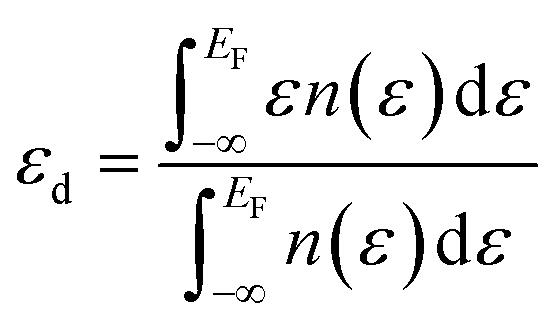 | (2) |
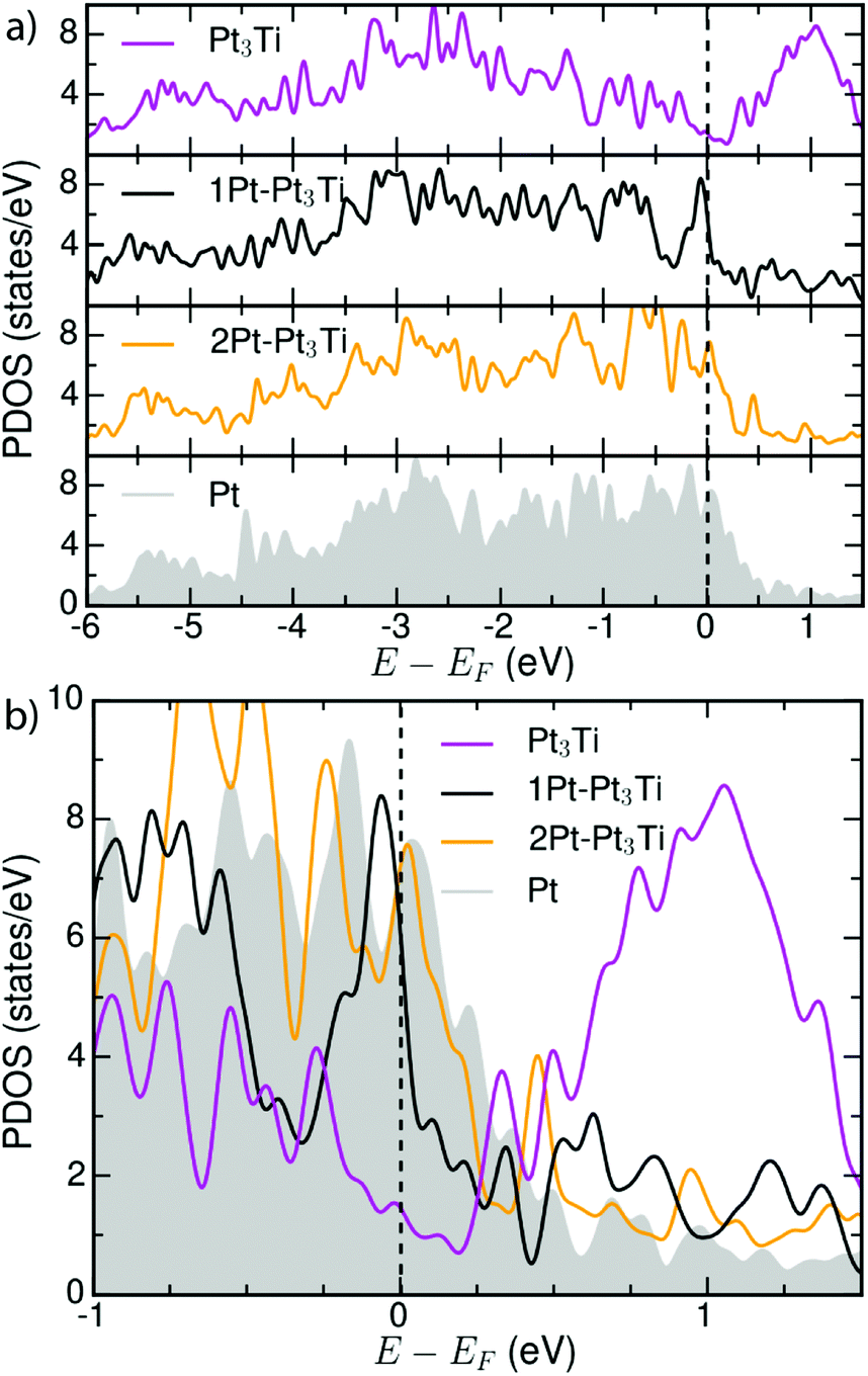 | ||
| Fig. 4 (a) Total d-PDOS used to calculate the d-band centers (εd) for Pt3Ti, Pt–Pt3Ti, 2Pt–Pt3Ti and Pt(111)-substrates (see Table 1). (b) Comparison of the total d-PDOS of the simulated terminations in the energy range around EF. | ||
Our calculated d-band center (εd) of the modeled surfaces (Table 1) agree well with those reported in ref. 5. Note that other simulations reported in literature1,4 using different methods or models assuming the second crystal layer to be composed of 50% Pt and 50% Ti atoms1,4 result in different d-band center energies for the Pt–Pt3Ti(111) termination and Pt(111). The difference between the d-band center of the bulk terminated Pt3Ti(111) surface and the pure Pt(111) surface obtained from our calculations, Δd-band = 0.43 eV, also corresponds to the experimentally obtained values2,38 pointing to the relevance of our model.
In view of the ‘volcano-type’ trend in the catalytic activity of the ORR in dependence of the d-band center, the Pt–Pt3Ti(111) termination would meet the assumed ideal shift of −0.2 eV relative to the d-band center of Pt(111). Indeed the ORR activity of this termination is increased relative to the bulk termination as proved experimentally.2 However, it does not meet the top of the volcano. This does not mean, that there is no correlation between the ORR activity and the d-band center or the related oxygen adsorption energy of the respective catalytic surfaces. In contrary, this correlation is theoretically and experimentally justified as far as alloy surfaces produced in the same way are compared.3,4,17 Though it points to the fact that the details of the surface termination depending on the production process of the electro catalysts are still poorly understood. Based on our findings the differences in the catalytic activity of assumed equal catalysts produced by different methods can be attributed to different surface terminations. Since the d-band center shifts dramatically if only one additional monolayer of Pt is added to the surface (see Table 1), the production process has to be monitored in more detail. It is essential to identify unambiguously the topmost three atomic layers of an alloy to be able to predict the electro chemical activity.
For practical application the optimization of the ORR activity, especially of dispersed nanoparticles, is of relevance.1,39 Here, UHV-STM methods are not applicable. However, Pt segregation to the outermost layer of the Pt3Ti(111) alloy is likely for Pt concentrations slightly higher than 75 at%.5 Moreover, based on our work, it can be assumed that this Pt segregation can be enhanced with increasing Pt concentration and a post-annealing step. Consequently, a possible optimization procedure for the ORR activity of any Pt3M alloy in any habit can be: change the composition of the alloy very carefully while the fabrication procedure is kept absolutely constant and measure the resulting ORR activity. Then the ORR activity should peak at one composition of the alloy that causes a distinct termination corresponding to an optimal d-band and thus, an optimal electro chemical activity.
Moreover, the d-band center is a reliable first measure, but it is not sufficient to describe all facets of the catalytic activity, since both, e.g. 2Pt–Pt3Ti and Pt, exhibit the same d-band center (see Table 1) but differ in ORR activity and stability.1,4,38 As described in very recent publications, especially the LDOS near the Fermi level (−0.5 eV < E − EF < 0.5 eV) for the surface Pt atoms is of importance for the oxygen adsorption energy and thus, for the ORR activity.40 This relationship is also in accordance with the total d-PDOS close to EF observed here: Pt3Ti < Pt–Pt3Ti < 2Pt–Pt3Ti(111)∼Pt(111). In Fig. 4(b) small differences between the d-PDOS of 2Pt–Pt3Ti(111) and Pt(111) close to the Fermi-level can be observed though similarities exist. In general, the density of states close to the Fermi level seems to be a superior measure for the catalytic activity of a bi- or trimetallic alloy than the d-band center.41
However, it is of great importance that the total d-PDOS close to the Fermi level (see Fig. 4) and the d-band center of Pt-alloys with 3d-transition metals depend on their exact surface termination, i.e. the composition of the three topmost layers of an alloy. Consequently, the surface electronic structure can be tuned intentionally by the surface termination. This opens up a new way to optimize the electrochemical activity of bi- or trimetallic catalysts.
Surface defects and segregation effects
As a result of our preparation conditions, that is, soft Ne+-sputtering at 1 × 10⁻⁵ mbar and subsequent annealing at 1200 K according to method 1, we obtain a termination of the Pt3Ti(111) single crystal by a monolayer of Pt, i.e. Pt–Pt3Ti (S1). Like already mentioned above, we receive large terraces with a homogeneous termination (Fig. 1). Due to the high regularity of the surface pattern defects with an apparent height of only 5–15 pm can be identified (Fig. 5). Two characteristic defects, a bright defect (D1) and a dark defect (D2), are shown in Fig. 5 at Vbias = 0.58 V and Vbias = 1.30 V, respectively. In consequence of D1 the triangles built by three Pt atoms in direct contact with a Ti atom in the second layer appear brighter at Vbias = 0.58 V, while at Vbias = 1.30 V the triangles located above a Ti atom in the third layer appear brighter. At the latter bias voltage mainly unoccupied delocalized electronic states at higher energy contribute to the apparent STM image. Thus, it is possible that here a defect in the third layer is monitored, which results in a lower energy of the unoccupied surface electronic states, like e.g. a Ti atom at the position of a Pt atom.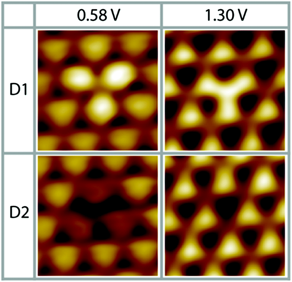 | ||
| Fig. 5 Two different characteristic surface defects on S1 (Pt–Pt3Ti), D1 and D2 (0.58 V, 0.48 nA; 1.30 V, 0.11 nA; low pass filtered; 1.7 nm × 1.7 nm). | ||
The dark defect is also monitored at Vbias = 0.58 V and Vbias = 1.30 V. In this case, the contrast in the STM image changes clearly due to D2 only at Vbias = 0.58 V, while D2 is almost not visible at Vbias = 1.30 V. At low positive bias unoccupied surface states mainly located near the surface are monitored. However, the apparent height difference between D2 and the surrounding features is so small that a defect in the topmost layer can be excluded. In consequence, a defect in the second layer causing a shift in the surface electronic states to higher energies can be assumed, like substitution of a Ti atom by a Pt atom or a vacancy. Thus, these STM images of defects recorded on the Pt–Pt3Ti surface confirm that the surface electronic structure is significantly influenced by small changes of the atomic composition in the second and third layer.
A defect in the topmost layer of the Pt–Pt3Ti surface is shown in Fig. 6. This sequence of STM images was taken at 77 K with a time difference of 170 s between two successive images. Although it is not possible to identify exactly the atomic transpositions since every bright feature corresponds to three Pt atoms, valuable insights into the segregation mechanism can be obtained from this STM sequence. First of all, it is remarkable that the segregation mechanism takes place even at a temperature of 77 K. This points to a large driving force for this process based on an energy gain related to a perfect Pt–Pt3Ti termination. Second, this segregation mechanism involves more than one layer, indicated by the contrast changes of the features in the topmost layer (see t = 3 and t = 4) due to transpositions in the second or third layer. Third, multiple small steps are involved in order to create a perfect Pt–Pt3Ti termination pointing to a thermodynamically activated process involving several equilibrium conditions. Thus, the Pt–Pt3Ti termination can be identified as thermodynamically stable surface state of a Pt3Ti single crystal with a small deficiency of Ti atoms.
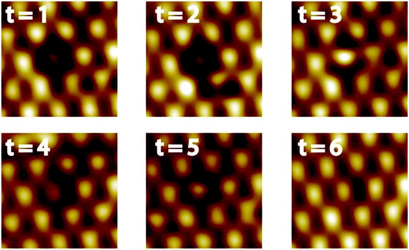 | ||
| Fig. 6 High-resolution UHV-STM images of Pt–Pt3Ti (2.1 nm × 2.1 nm) showing the healing process of a defect by restructuring (T = 77 K). Time difference between two following STM images: Δt = 170 s (0.94 V; 0.08 nA, low pass filtered). | ||
Conclusions
In conclusion, we introduced a method, combining voltage dependent imaging and simulated STM maps based on ab initio DFT calculations that allows us to identify the exact surface termination in the case of the bimetallic Pt3Ti alloy. We could show that, depending on the crystal preparation by a reproducible sputtering/annealing method, two distinct terminations of the Pt3Ti(111) single crystal surface are created, i.e. one monolayer of Pt (Pt–Pt3Ti(111)) or two Pt layers covering the bulk crystal (2Pt–Pt3Ti(111)). Furthermore, the surface electronic structure, characterized by the d-band center and the total d-PDOS close to the Fermi level, depends sensitively on the exact surface termination. Thus, the catalytic activity of the bimetallic alloy can be tuned intentionally by creating a distinct surface termination. Even small changes of the atomic composition in the second and third layer of the crystal result in changes of the surface electronic structure as proven by our STM images of defects. Based on our investigations we can state that further insights into the relationship between production procedures of bimetallic alloys and their respective resulting surface termination are needed in order to systematically optimize their catalytic activity.Acknowledgements
The authors gratefully acknowledge the help of Jochen Friedrich and Stephan Masberg. M.P. would like to thank Paul Meuffels for helpful discussions. Computations were carried out using the high performance computer JUQUEEN operated by the Jülich Supercomputing Centre (JSC) at the Forschungszentrum Jülich. N. A., V. C., and S. K. gratefully acknowledge financial support from the Volkswagen–Stiftung through the “Optically Controlled Spin Logic” project.References
- H. Duan, Q. Hao and C. Xu, J. Power Sources, 2015, 280, 483–490 CrossRef CAS.
- V. R. Stamenkovic, B. S. Mun, M. Arenz, K. J. J. Mayrhofer, C. A. Lucas, G. Wang, P. N. Ross and N. M. Markovic, Nat. Mater., 2007, 6, 241–247 CrossRef CAS PubMed.
- J. Greeley, I. E. L. Stephens, A. S. Bondarenko, T. P. Johansson, H. A. Hansen, T. F. Jaramillo, J. Rossmeisl, I. Chorkendorff and J. K. Norskov, Nat. Chem., 2009, 1, 552–556 CrossRef CAS PubMed.
- V. Stamenkovic, B. S. Mun, K. J. J. Mayrhofer, P. N. Ross, N. M. Markovic, J. Rossmeisl, J. Greeley and J. K. Norskov, Angew. Chem., Int. Ed., 2006, 118, 2963–2967 CrossRef.
- Z. Duan, J. Zhong and G. Wang, J. Chem. Phys., 2010, 133, 114701 CrossRef PubMed.
- A. Stassi, C. d'Urso, V. Baglio, A. di Blasi, V. Antonucci, A. S. Arico, A. M. Castro Luna, A. Bonesi and W. E. Triaca, J. Appl. Electrochem., 2006, 36, 1143–1149 CrossRef CAS.
- W. Chen, J. A. K. Paul, A. Barbieri, M. A. van Hove, S. Cameron and D. J. Dwyer, J. Phys.: Condens. Matter, 1993, 5, 4585–4594 CrossRef CAS.
- W. Chen, L. Severin, M. Göthelid, M. Hammar, S. Cameron and J. Paul, Phys. Rev. B: Condens. Matter, 1994, 50, 5620–5627 CrossRef CAS.
- M. A. Vasiliev, J. Phys. D: Appl. Phys., 1997, 30, 3037–3070 CrossRef CAS.
- H.-C. Tsai, T. H. Yu, Y. Sha, B. V. Merinov, P.-W. Wu, S.-Y. Chen and W. A. Goddard, J. Phys. Chem. C, 2014, 118, 26703–26712 CAS.
- W. Yu, M. D. Porosoff and J. G. Chen, Chem. Rev., 2012, 112, 5780–5817 CrossRef CAS PubMed.
- T. H. Yu, T. Hofmann, Y. Sha, B. V. Merinov, D. J. Myers, C. Heske and W. A. Goddard, J. Phys. Chem. C, 2013, 117, 26598–26607 CAS.
- S. Le Moal, M. Moors, J. M. Essen, C. Breinlich, C. Becker and K. Wandelt, J. Phys.: Condens. Matter, 2013, 25, 045013 CrossRef PubMed.
- S. Le Moal, M. Moors, J. M. Essen, C. Becker and K. Wandelt, Surf. Sci., 2010, 604, 1637–1644 CrossRef CAS.
- S. Ringler, E. Janin, M. Boutonnet-Kizling and M. Gothelid, Appl. Surf. Sci., 2000, 162, 190–197 CrossRef.
- W. Chen, E. Chulkovl and J. Paul, Phys. Scr., 1996, 54, 392–396 CrossRef CAS.
- S. Kattel, Z. Duan and G. Wang, J. Phys. Chem. C, 2013, 117, 7107–7113 CAS.
- C. Breinlich, M. Buchholz, M. Moors, S. Le Moal, C. Becker and K. Wandelt, J. Phys. Chem. C, 2014, 118, 6186–6192 CAS.
- P. Hohenberg and W. Kohn, Phys. Rev., 1964, 136, B864–B871 CrossRef.
- P. E. Blöchl, Phys. Rev. B: Condens. Matter, 1994, 50, 17953–17979 CrossRef.
- G. Kresse and J. Hafner, Phys. Rev. B: Condens. Matter, 1994, 49, 14251–14269 CrossRef CAS.
- G. Kresse and J. Hafner, Phys. Rev. B: Condens. Matter, 1996, 54, 11169–11186 CrossRef CAS.
- J. P. Perdew, K. Burke and M. Ernzerhof, Phys. Rev. Lett., 1996, 77, 3865–3868 CrossRef CAS PubMed.
- U. Starke, J. B. Pendry and K. Heinz, Prog. Surf. Sci., 1996, 52, 53–124 CrossRef CAS.
- G. Betz, Surf. Sci., 1980, 92, 283–309 CrossRef CAS.
- M. Schmid, A. Biedermann, H. Stadler and P. Varga, Phys. Rev. Lett., 1992, 69, 925–928 CrossRef CAS PubMed.
- M. Schmid, A. Biedermann, C. Slama, H. Stadler, P. Weigand and P. Varga, Nucl. Instr. Meth. B, 1993, 82, 259–268 CrossRef CAS.
- V. S. Smentkowski, Prog. Surf. Sci., 2000, 64, 1–58 CrossRef CAS.
- N. Laegreid and G. K. Wehner, J. Appl. Phys., 1961, 32, 365–369 CrossRef CAS.
- R. Behrisch and W. Eckstein, Sputtering by Particle Bombardment, Springer, Heidelberg, 2007 Search PubMed.
- P. Sigmund, Phys. Rev., 1969, 184, 383–416 CrossRef CAS.
- P. Süle, M. Menyhard, L. Kotis, J. Labar and W. F. Egelhoff, J. Appl. Phys., 2007, 101, 043502 CrossRef.
- B. Voigtländer, Scanning Probe Microscopy, Springer, Berlin, 2015 Search PubMed.
- M. C. Lennartz, V. Caciuc, N. Atodiresei, S. Karthäuser and S. Blügel, Phys. Rev. Lett., 2010, 105, 066801 CrossRef CAS PubMed.
- M. C. Lennartz, N. Atodiresei, V. Caciuc and S. Karthäuser, J. Phys. Chem. C, 2011, 115, 15025–15030 CAS.
- Y. Kuk and P. J. Silverman, J. Vac. Sci. Technol., A, 1990, 8, 289–292 CAS.
- J. A. Stroscio, D. T. Pierce, A. Davies and R. J. Celotta, Phys. Rev. Lett., 1995, 75, 2960–2963 CrossRef CAS PubMed.
- S. J. Hwang, S.-K. Km, J.-G. Lee, S.-C. Lee, J. H. Jang, P. Kim, T.-H. Lim, Y.-E. Sung and S. J. Yoo, J. Am. Chem. Soc., 2012, 134, 19508–19511 CrossRef CAS PubMed.
- T. Gunji, T. Tanabe, G. Saravanan, S. Kaneko, H. Yoshikawa, Y. Matsushita, N. Sekido, Y. Xu, S. Ueda, H. Abe and F. Matsumoto, Electrochemistry, 2015, 83, 7–11 CrossRef CAS.
- C.-E. Kim, D.-H. Lim, J. H. Jang, H. J. Kim, S. P. Yoon, J. Han, S. W. Nam, S.-A. Hong, A. Soon and H. C. Ham, J. Chem. Phys., 2015, 142, 034707 CrossRef PubMed.
- M. T. Gorzkowski and A. Lewera, J. Phys. Chem. C, 2015, 119, 18389–18395 CAS.
Footnote |
| † Electronic supplementary information (ESI) available. See DOI: 10.1039/c5nr08420b |
| This journal is © The Royal Society of Chemistry 2016 |