
 Open Access Article
 This Open Access Article is licensed under a Creative Commons Attribution-Non Commercial 3.0 Unported Licence
Defect segregation and optical emission in ZnO nano- and microwires†
W. T.
Ruane
*a,
K. M.
Johansen
b,
K. D.
Leedy
c,
D. C.
Look
cd,
H.
von Wenckstern
e,
M.
Grundmann
e,
G. C.
Farlow
f and
L. J.
Brillson
g
aDepartment of Physics, The Ohio State University, Columbus, Ohio 43210, USA. E-mail: ruane.3@osu.edu
bUniversity of Oslo, Centre for Materials Science and Nanotechnology, 0318 Oslo, Norway
cAir Force Research Laboratory, Sensors Directorate, WPAFB, OH 45433, USA
dSemiconductor Research Center, Wright State University, Dayton, OH 45435, USA
eInstitut für Experimentelle Physik II, Universität Leipzig, Linnéstr. 5, 04103 Leipzig, Germany
fDepartment of Physics, Wright State University, Dayton, OH 45435, USA
gDepartment of Physics and Department of Electrical & Computer Engineering, The Ohio State University, Columbus, OH 43210, USA
First published on 11th March 2016
Abstract
The spatial distribution of defect related deep band emission has been studied in zinc oxide (ZnO) nano- and microwires using depth resolved cathodoluminescence spectroscopy (DRCLS) in a hyperspectral imaging (HSI) mode within a UHV scanning electron microscope (SEM). Three sets of wires were examined that had been grown by pulsed laser deposition or vapor transport methods and ranged in diameter from 200 nm–2.7 μm. This data was analyzed by developing a 3D DRCLS simulation and using it to estimate the segregation depth and decay profile of the near surface defects. We observed different dominant defects from each growth process as well as diameter-dependent defect segregation behavior.
Introduction
Research interest in the II–VI compound semiconductor ZnO continues to grow for next generation opto- and microelectronics based on its wide band gap (3.37 eV), large exciton binding energy (60 meV), low cost, ease of growth and etching, and biocompatibility.1–4 Among extensive studies of this material, there is increasing interest in ZnO nanostructures, which have already demonstrated their utility as field effect transistors, optically pumped lasers, photodetectors, batteries, chemical and biological sensors.5–9 Achievable through different growth conditions, these nanostructures display a wide variety of morphologies, including: nano- and microwires, tetrapods, needles, and helix structures.10,11 In general, the balance of different defects and dopants in a semiconductor bulk material is detrimental to its behavior. Thus fundamental understanding of defect and dopant interaction has been one of the key elements in semiconductor research for the last 60 years. This also holds when utilizing micro- and nanowires.Previous studies on defect distribution in ZnO wires have reported defect segregation where defects are located at or near the nanowire surfaces.12–15 CL spectra of microwires grown by pulsed laser deposition (PLD) on sapphire displayed impurity emissions near the surface on a submicron scale in cross section.14 Transport and photoluminescence (PL) studies of similar nanowires with diameters ranging from 0.1 to 7.5 μm supported a core–shell model and showed that intentional Al doping could decrease resistivity by two orders of magnitude.15 Shalish et al.12 used PL to study sets of different diameter (50 nm–300 nm) nanowires and observed a linear increase in the ratio of the near band edge to green band defect (Inbe/Igb) peak intensities with increasing diameter. This increase was attributed to high defect densities at the surface of the wires and that holes within 30 nm of the surface would diffuse and recombine there. Xue et al.13 used spatially resolved cathodoluminescence across a 180 nm diameter nanowire. These data were analyzed using a constant-density core–shell model, consisting of a high defect density shell and a lower defect density core. The thickness of the shell was estimated at 5–6 nm.
The direct approach to obtain the defect distribution of the cross section of a wire is to cut the wire and measure across the resulting plane. However, this process will damage the wire and can distort the intended measurement in terms of altered strain, shape, defect distribution, and density. Furthermore, it is not suitable for in situ characterization. Thus there is a need for a non-destructive method to extract the depth dependent information.
In our study, nano- and microwires grown by a variety of methods were measured by DRCLS, in hyperspectral mode, across the outside walls of the wires. To reconstruct the spatial defect variation along the cross section of the wire, a 3D DRCLS simulation and defect model was developed. The results reveal segregation of defects towards the surface, and both the defect distribution profile and segregation depth have been extracted.
Experiment
In this study, we performed DRCLS on three different sets of ZnO wires grown by different methods and with a wide range of wire diameters. In DRCLS measurements, a constant-energy beam of electrons is directed toward a sample where these fast electrons lose energy as they travel through and interact with the target. Eventually, this energy loss causes the generation of electron–hole (e–h) pairs closely following the energy loss profile of the fast electrons. Thus, the region in which e–h pairs are generated depends on the beam-spot size and energy. The minority carriers (holes in n-type ZnO), which are a rate limiting factor for recombination, may diffuse and/or drift in the sample before recombination occurs either by a radiative or non-radiative process. Light emitted by radiative recombination of these e–h pairs is collected by a parabolic mirror, then passed into a monochromator and CCD camera, then digitized as a spectrum of intensity vs. wavelength (or energy). The features in these spectra can reveal information about the electronic structure in the material, including the bandgap and crystal defect states. For in depth information about the measurement and physical processes involved in cathodoluminescence, interested readers are referred to, e.g., Yacobi et al.16The measurements in this study were performed on a JEOL 7800f UHV SEM which has been modified for cathodoluminescence. We use an Oxford MonoCL monochromator outfitted with a Gatan grating (150 lines per mm and blaze wavelength of 500 nm) and an Andor Newton CCD camera. This setup allowed us to capture hyperspectral images (HSI) by using a DAC card to control the SEM beam location with special software (CHIMP).17 Each HSI consists of a 2D rectangular array of cathodoluminescence spectra, where each point in the array corresponds to a spatial location on the sample that the electron beam dwells on for a fixed time. All measurements were taken at a temperature of 80 K.
The hyperspectral images were captured using an electron beam energy of 5 keV on a variety of wires from each sample set. This probe energy was chosen because it struck a good balance between high signal counts and good spatial resolution, allowing for high density HSI's to be captured in a reasonable amount of time. Although most SEMs have a spot-size on the order of a few nanometers, higher beam energy results in larger generation volumes of e–h pairs under the surface. This reduces the spatial resolution of the CL measurement.
The three sets of ZnO wires varied in growth method, size, and type of defects. Wire set A was grown by PLD and had a hexagonal prism geometry ranging in diameter from 100 nm–10 μm. Many of these wires were quite long (>100 μm) and straight. Set B was grown using CVD and consisted of needle-shaped wires and larger hexagonal prism shaped wires (400 nm–2 μm in diameter). These wires were shorter than set A, usually <10 μm. Set C was grown by PLD by using a target consisting of ZnO![[thin space (1/6-em)]](https://www.rsc.org/images/entities/char_2009.gif) :Ga2O3/99:1wt%. The wires from set C were approximately 2 μm in length and 200 nm in diameter. Their width was too small to acquire detailed enough DRCLS HSI line-scans needed for an analysis of their spatial defect distribution.
:Ga2O3/99:1wt%. The wires from set C were approximately 2 μm in length and 200 nm in diameter. Their width was too small to acquire detailed enough DRCLS HSI line-scans needed for an analysis of their spatial defect distribution.
Model & DRCLS simulation
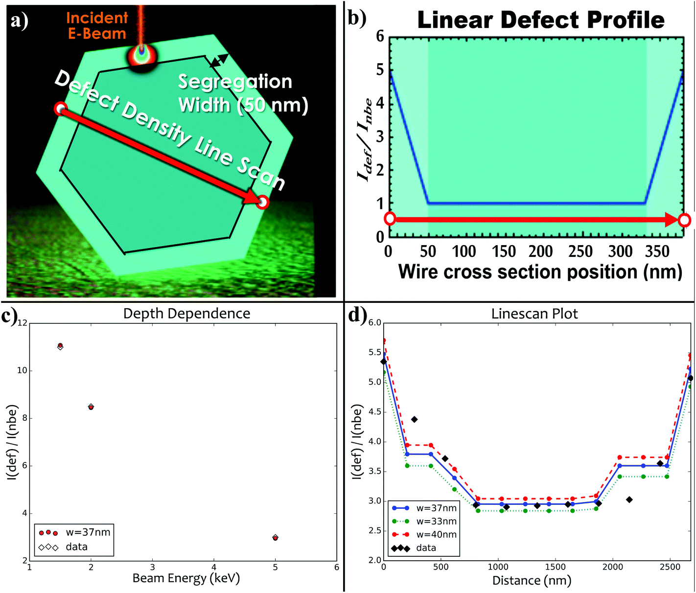
When analyzing the DRCLS HSI data of different wires, the ratio of the defect peak to the NBE (Idef/Inbe) vs. distance across the wire diameter (line-scan) was studied. The red arrow on the SEM image in Fig. 1(a), a ZnO wire from set A, represents the path of a typical line-scan. These line-scans were found to have relatively high values near the edges of the wire and dropped to lower values toward the center. This behavior is consistent with the defects segregating towards the free surface since the electron beam samples more of the surface region at the edges of a wire vs. near the wire's center (see Fig. 1 for details). Despite this general trend, the shapes of these line profile plots varied between wires and were often asymmetrical. Thus, to be able to extract information about the defect distribution, a DRCLS simulation was developed (see below). This simulation enabled us to reproduce the observed variations and asymmetries, supporting the validity of our model and our estimates of the physical parameters involved. | ||
| Fig. 1 (a) Illustration showing the line-scan measurement process and an SEM picture of a ZnO wire. The red arrow in the SEM image represents a typical line-scan path discussed in this paper. Geometrical parameters of the wire are also shown. (b) Illustration of simulation for a scan point. | ||
We modeled the defect distribution as a function defined within a hexagonal prism with the origin of the coordinate system at the center of the hexagon. The x-axis lies parallel to the plane of the sample holder, the y-axis is parallel to the wire's c-axis, and the z-axis’ direction points toward the collection mirror above the wire. The cross section of the prism is a regular hexagon whose geometrical parameters (Fig. 1(a)), r (radius) & θ (tilt angle), can be extracted from a secondary electron image (SEI). This can be done by measuring the distance between the vertices, as viewed from above, and using some basic geometry (see the ESI† for more details). The value of the defect density at a point is determined by a piecewise function defined in two regions we refer to as the segregation region and the bulk region. The bulk region domain lies in a smaller, concentric, hexagonal prism of radius b. This radius b is determined so that the separation between the inner and outer prisms is the segregation width, wseg. If the point lies within the bulk region the density is given by cbulk. If the point lies outside the smaller hexagonal prism, but still within the bounding prism (i.e., in the segregation region) then the density is determined by some function of the distance from that point to the bounding hexagonal prism's surface. The functions we used to model the defect density in the segregation region were: a constant value (csurf), linear decay, and exponential decay. The linear and exponential decay profiles had a value of csurf on the surface and reached a value of cbulk a distance wseg below the free surface. An illustration of a linear decay profile is shown in Fig. 2.
 | ||
| Fig. 2 (a) Cross section view of ZnO wire showing how the defect line scan plot in (b) is mapped onto physical space. (b) Illustration of how defects vary across a wire's cross section for a linear decay profile. (c) Single spot depth dependence measurement on a ZnO wire's top face (d) Corresponding 5 keV line-scan fit for wire from (c) (blue dots represent the best fit). | ||
The CL simulation uses 3D energy loss profiles (ELP) generated by the software CASINO (monte CArlo Simulation of electroN trajectory in sOlids).18 This software allows one to create/import a 3D model of a sample, subdivide it into small rectangular prisms (cells), and then track the energy lost within each cell as the trajectories of the incident electrons are calculated (Fig. 1(b)). The CL simulation software developed here then iterates through each of the cells and divides the energy absorbed, ΔEij, by an average ionization energy to find the number of e–h pairs (ELP) generated in cell  .
.
The main effect of minority carrier diffusion is to expand the CL probing volume (where light is emitted from). This is simulated, in a rather simplistic way, by doing a 2D Gaussian convolution with the ELP calculated distribution of holes (minority carriers in n-type ZnO). The result of the convolution is a new hole distribution, which represents the spatial distribution of where radiative recombination will occur. The Gaussian's variance is set by the minority carrier diffusion length and any hole ending up outside of the wire is assumed to have recombined at the surface. There are several potential improvements that can be made to such a model, e.g., by including a diffusion length which is a function of the local defect densities instead of a single parameter. However, as discussed below, allowing for a single parameter minority carrier diffusion did not improve our overall fit to the experimental curves for our data. Hence, the development of the method has not been pursued further at this stage.
The number of holes that recombine through a defect state (Ndef) or as a near band edge (Nnbe) emission is governed by the local value of the defect concentration in our model. If Ndef and Nnbe photons are generated, the number of photons reaching the detector will be attenuated by their respective exponential factors e−α(f)zij, where zij is the distance from the cell to the surface and α(f) is the frequency dependent absorption coefficient. Adding up all the absorption-corrected photon count from each cell, one obtains the measured defect emission (Idef) & NBE emission (Inbe) intensities. The ratio is finally taken to give a value for Idef/Inbe for each electron beam spot.
As a test of the simulation and model we compared the results of a best fit using a 5 keV line-scan to that of the best fit of a CL depth dependence using three different beam energies (1.5 keV, 2 keV, and 5 keV) at a spot on the top face of the same, 2.7 μm diameter, wire. The current of the electron beam was set to maintain constant power throughout the 3 different probe energies. The best fit parameters (wseg, cbulk, & decay profile) were found to be the same for both the single-spot depth dependence fit (red dots in Fig. 2(c)) and the line-profile fit at 5 keV (blue dots in Fig. 2(d)), demonstrating the consistency and reliability of the method. The best fit parameters for the wire were, wseg = 37 nm and a linear decay profile, which is similar to the other micron-sized diameter wires from set A, which are presented in the results section.
Results and discussion
Fig. 3 shows examples of the CL-spectra obtained from the different sets of nano- and microwires. All spectra show the emission from the near band edge peak (NBE) (3.32 eV–3.37 eV) and its 2nd order replica, however, they show different deep level peaks. In set A, the spectra were dominated by what is often referred to in the literature as the structured green band.3 This defect emission is attributed to Cu2+ on a Zn site and can be recognized in a spectrum as a wide peak centered ∼2.35 eV with many, equally spaced (in energy), bump-like features.19 This can be fit to a Pekarian function whose intensity is given by,where S is the Huang Rhys factor, a measure of the strength of the phonon coupling, and n is the number of phonons involved in the transition. Our fit indicated an S value of 6.5, a zero-phonon line at 2.82 eV, and spacing of 70 meV. These values are, within the experimental error, consistent with the literature values of ZPL of 2.86 eV S = 6.5 and spacing of 72 meV.3,20

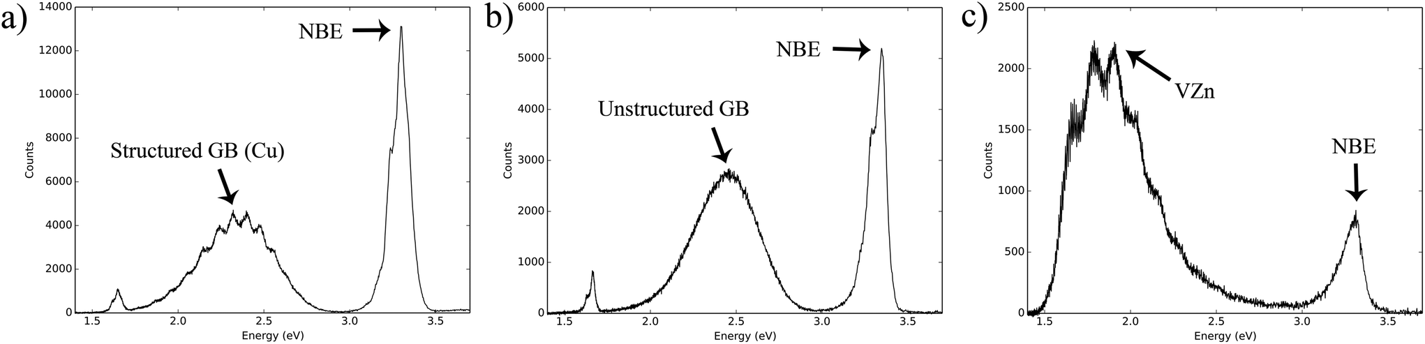 | ||
| Fig. 3 (a) CL spectrum from set A (CuZn). (b) CL spectrum from set B (UGB). (c) CL spectrum from set C (VZn). | ||
In set B, the deep band emission was primarily from an unstructured green band (UGB) emission. This appears in spectra as a smooth wide peak centered ∼2.45 eV. The nature of this peak is still contested but has been attributed to a variety of defects including Vo,21,22VZn,23 as well as other possibilities.3,24
In set C (Ga-doped ZnO wires), the defect emission peak energy was approximately 1.8 eV. Previous studies have correlated the emission for this energy to VZn isolated defects and defect clusters.25,26 That would be consistent with findings of acceptor compensation in highly n-type doped samples.27,28
We found that the defect segregation widths as well as their functional profiles were different for small diameter wires, e.g., 380 nm, compared to the larger, 1–2 μm diameter micowires. Fig. 4 illustrates the experimental line-scan values obtained from the HSI maps along with CL simulations that best fit the data points as determined by the least squares fit between simulated and the measured line-scans. Note how the simulations appear to reflect the asymmetries and slope changes of the experimental data. Bracketing each best fit simulation curve are alternate simulations with the same line profile but different wseg that establish error bounds. The following Error analysis section describes how best fits and their error bars are determined.
 | ||
| Fig. 4 DRCLS line-scan plots showing simulation's best fit (blue lines), error bounds (green & red lines), and measured data (black diamonds) for (a) 1.7 μm wire (b) 2.2 μm wire and (c) 380 nm wire. The segregation width (w) is included for each fit. | ||
Fig. 4(a) shows results for a 1.7 μm diameter wire from set B, whose dominant defect was the UGB. Here, wseg = 36 nm+9 nm−8 nm with a linear decay profile. Fig. 4(b) shows results for a much larger wire, a 2.2 μm diameter wire from set A, whose best fit profile corresponded to wseg = 36 nm ± 5 nm and a linear decay profile. The behavior of this defect was very similar to the 1.7 μm wire from set B. For both of the set A wires analyzed, we attributed the dominant defect to CuZn defects due to the phonon structure observed, given previous literature and since Cu can be a common trace impurity in ZnO. Fig. 4(c) shows results for the smallest wire studied, a 380 nm diameter from set A. The best fit obtained from our simulation yielded a segregation width wseg = 12 nm+6 nm−4 nm. This smallest experimental wire profile displayed closest agreement to the simulation profile for a constant decay type. Our best fits were achieved by neglecting a single parameter minority carrier diffusion length. A more extensive approach involving variable diffusion lengths through a Monte Carlo approach requires considerably more computational power and cost. However, our results recreating the line scans with no diffusion suggests, possibly due to high defect densities, that minority carrier diffusion near the surface may be small.
The profiles of the Idef/Inbe from our CL line-scans across the measured ZnO wires and the different segregation widths for different diameter wires are inconsistent with a defect emission process where minority carriers diffuse to the surface and recombine there. Thus our results show that there are defects below the surface of these structures, which may be of great importance in evaluating and improving the performance of devices based on ZnO.
Error analysis
Best fit calculations involved fixing csurf and varying the other parameters, as well as the profile types (constant, linear, and exponential), to find the combination that minimized the sum of the squared differences between the simulated and the measured line-scans. If the values of csurf and cbulk were both allowed to vary, the best fit was not well determined. The value of csurf was chosen to be fixed because, although cbulk can't be directly measured, the first few nanometers near the surface can be probed using low energy electrons. The error bounds assigned to our best fit's segregation width are to be understood within the context of our model and simulation. Assigning error bars on a Monte Carlo simulation is difficult and often ad hoc. The bounds here simply signify that outside these values we no longer consider it a good fit within our model (see Fig. 4).Conclusion
Defect segregation below the free surface was observed in ZnO nano- and microwires grown under different conditions and using different methods using a non-destructive approach. A 3D DRCLS simulation/model was developed and used to estimate the segregation width and decay profiles with 8–10 nm precision for these near-surface defects.We observed indications of a diameter dependence in this defect segregation behavior. These results support a model in which defects are distributed inside ZnO nano- and micowires and segregate towards free surfaces versus models in which carriers diffuse to recombination centers at the surface. The presence of electrically-active defects inside, rather than just on the surface, could affect electrical transport through such wires.
Acknowledgements
The authors gratefully acknowledge National Science Foundation, Grant No. DMR-1305193 (Charles Ying and Haiyan Wang), Deutsche Forschungsgemeinschaft (Gr 1011/26-1), and the Norwegian Research council (DYNAZOx, Project no. 221992), for support of this work. We would also like to thank Paul Edwards for his help setting up our DRCLS HSI capability.References
- S. J. Pearton, D. P. Norton, K. Ip, Y. W. Heo and T. Steiner, Recent Progress in Processing and Properties of ZnO, Prog. Mater. Sci., 2005, 50, 293, DOI:10.1016/j.pmatsci.2004.04.001.
- B. Claflin and D. C. Look, Electrical transport properties in zinc oxide, in ZnO Materials for Electronic and Optoelectronic Device Applications, ed. C. W. Litton, D. C. Reynolds and T. C. Collins, Wiley, New York, 2011, p. 61, DOI:10.1002/9781119991038.
- U. Ozgur, Ya. I. Alivov, C. Liu, A. Teke, M. A. Reshchikov, S. Doan, V. Avrutin, S.-J. Cho and H. Morkoc, A comprehensive review of ZnO materials and devices, J. Appl. Phys., 2005, 98, 041301, DOI:10.1063/1.1992666.
- A. Janotti and C. G. Van de Walle, Fundamentals of zinc oxide as a semiconductor, Rep. Prog. Phys., 2009, 72, 126501, DOI:10.1088/0034-4885/72/12/126501.
- A. B. Djurisic and Y. H. Leung, Optical Properties of ZnO Nanostructures, Small, 2006, 2, 944, DOI:10.1002/smll.200600134.
- S. Chu, G. Wang, W. Zhou, Y. Lin, L. Chernyak, J. Zhao, J. Kong, L. Li, J. Ren and J. Liu, Electrically-pumped waveguide lasing from ZnO nanowires, Nat. Nanotechnol., 2011, 6, 506, DOI:10.1038/NNANO.2011.97.
- B. S. Kang, H. T. Wang, F. Ren and S. J. Pearton, Electrical detection of biomaterials using AlGaN/GaN high electron mobility transistors, J. Appl. Phys., 2008, 104, 031101, DOI:10.1063/1.2959429.
- C. Soci, A. Zhang, B. Xiang, S. A. Dayeh, D. P. R. Aplin, J. Park, X. Y. Bao, Y. H. Lo and D. Wang, ZnO Nanowire UV Photodetectors with High Internal Gain, Nano Lett., 2007, 7, 1003, DOI:10.1021/nl070111x.
- M. Willander, O. Nur, J. R. Sadaf, M. I. Qadir, S. Zaman, A. Zainelabdin, N. Bano and I. Hussain, Luminescence from Zinc Oxide Nanostructures and Polymers and their Hybrid Devices, Materials, 2010, 3, 2643, DOI:10.3390/ma3042643.
- L. Schmidt-Mende and J. L. MacManus-Driscoll, ZnO nanostructures, defects, and devices, Mater. Today, 2007, 10, 40, DOI:10.1016/S1369-7021(07)70078-0..
- C. Jagadish and S. J. Pearton, Zinc Oxide Bulk, Thin Films and Nanostructures: Processing, Properties, and Applications, Elsevier Science, 2006, ISBN: 9780080447223 Search PubMed.
- I. Shalish, H. Temkin and V. Narayanamurti, , Size-dependent surface luminescence in ZnO nanowires, Phys. Rev. B: Condens. Matter, 2004, 69, 245401, DOI:10.1103/PhysRevB.69.245401.
- H. Xue, N. Pan, R. Zeng, M. Li, X. Sun, Z. Ding, X. Wang and J. G. Hou, Probing the Surface Effect on Deep-Level Emissions of an Individual ZnO Nanowire via Spatially Resolved Cathodoluminescence, J. Phys. Chem. C, 2009, 113(29), 12715–12718, DOI:10.1021/jp903690g.
- T. Nobis, E. M. Kaidashev, A. Rahm, M. Lorenz, J. Lenzner and M. Grundmann, Spatially Inhomogeneous Impurity Distribution in ZnO Micropillars, Nano Lett., 2004, 4, 797, DOI:10.1021/nl049889y.
- G. Zimmermann, M. Lange, B. Cao, M. Lorenz and M. Grundmann, Resistivity control of ZnO nanowires by Al doping, Phys. Status Solidi, 2010, 4, 82, DOI:10.1002/pssr.201004015.
- B. G. Yacobi and D. B. Holt, Cathodoluminescence scanning electron microscopy of semiconductors, J. Appl. Phys., 1986, 59, R1, DOI:10.1063/1.336491.
- P. R. Edwards, L. K. Jagadamma, J. Bruckbauer, C. Liu, P. Shields, D. Allsopp, T. Wang and R. W. Martin, High-Resolution Cathodoluminescence Hyperspectral Imaging of Nitride Nanostructures, Microsc. Microanal., 2012, 18(6), 1212–1219 CrossRef CAS PubMed.
- D. Drouin, CASINO a Powerful Simulation Tool for Cathodoluminescence Applications, Microsc. Microanal., 2006, 12(Suppl. 02), 1512–1513, DOI:10.1017/S1431927606069686.
- R. Dingle, Luminescent Transitions Associated With Divalent Copper Impurities and the Green Emission from Semiconducting Zinc Oxide, Phys. Rev. Lett., 1969, 23, 579, DOI:10.1103/PhysRevLett.23.579.
- D. Byrne, F. Herklotz, M. O. Henry and E. McGlynn, Unambiguous identification of the role of a single Cu atom in the ZnO structured green band, J. Phys.: Condens. Matter, 2012, 24, 215802 CrossRef CAS PubMed.
- K. Vanheusden, C. H. Seager, W. L. Warren, D. R. Tallant and J. A. Voigt, Appl. Phys. Lett., 1996, 68, 403, DOI:10.1063/1.116699.
- X. J. Wang, L. S. Vlasenko, S. J. Pearton, W. M. Chen and I. A. Buyanova, Oxygen and zinc vacancies in as-grown ZnO single crystals, J. Phys. D: Appl. Phys., 2009, 42, 174411, DOI:10.1088/0022-3727/42/17/.
- F. Fabbri, M. Villani, A. Catellani, A. Calzolari, G. Cicero, D. Calestani, G. Calestani, A. Zappettini, B. Dierre, T. Sekiguchi and G. Salviati, Zinc vacancy induced green luminescence on non-polar surfaces in ZnO nanostructures, Sci. Rep., 2010, 4, 5158, DOI:10.1038/srep05158.
- B. Lin, Z. Fu and Y. Jia, Green luminescent center in undoped zinc oxide films deposited on silicon substrates, Appl. Phys. Lett., 2001, 79, 943, DOI:10.1063/1.13941.
- Y. Dong, F. Tuomisto, B. G. Svensson, A. Yu. Kuznetsov and L. J. Brillson, Vacancy Defect and Defect Cluster Energetics In Ion-implanted ZnO, Phys. Rev. B: Condens. Matter, 2010, 81, 081201(R), DOI:10.1103/PhysRevB.81.081201.
- K. E. Knutsen, A. Galeckas, A. Zubiaga, F. Tuomisto, G. C. Farlow, B. G. Svensson and A. Yu. Kuznetsov, Zinc vacancy and oxygen interstitial in ZnO revealed by sequential annealing and electron irradiation, Phys. Rev. B: Condens. Matter, 2012, 86, 121203(R), DOI:10.1103/PhysRevB.86.121203.
- D. C. Look, K. D. Leedy, L. Vines, B. G. Svensson, A. Zubiaga, F. Tuomisto, D. R. Doutt and L. J. Brillson, Self-compensation in semiconductors: the Zn-vacancy in Ga-doped ZnO, Phys. Rev. B: Condens. Matter, 2011, 84, 115202, DOI:10.1116/1.1394728.
- K. M. Johansen, A. Zubiaga, I. Makkonen, F. Tuomisto, P. T. Neuvonen, K. E. Knutsen, E. V. Monakhov, A. Yu. Kuznetsov and B. G. Svensoon, Identification of substitutional Li in n-type ZnO and its role as an acceptor, Phys. Rev. B: Condens. Matter, 2011, B83, 245208, DOI:10.1103/PhysRevB.83.245208.
Footnote |
| † Electronic supplementary information (ESI) available. See DOI: 10.1039/C5NR08248J |
| This journal is © The Royal Society of Chemistry 2016 |