
 Open Access Article
 This Open Access Article is licensed under a
 Creative Commons Attribution 3.0 Unported Licence
Energy band diagram of device-grade silicon nanocrystals†
M.
Macias-Montero
*a,
S.
Askari
a,
S.
Mitra
a,
C.
Rocks
a,
C.
Ni
b,
V.
Svrcek
c,
P. A.
Connor
b,
P.
Maguire
a,
J. T. S.
Irvine
b and
D.
Mariotti
a
aNanotechnology & Integrated Bio-Engineering Centre (NIBEC), University of Ulster, BT37 0QB, UK. E-mail: m.macias-montero@ulster.ac.uk
bSchool of Chemistry, University of St Andrews, St Andrews, Fife, KY16 9ST, UK
cResearch Center for Photovoltaic Technologies, National Institute of Advanced Industrial Science and Technology (AIST), Tsukuba, 305-8568, Japan
First published on 23rd February 2016
Abstract
Device grade silicon nanocrystals (NCs) are synthesized using an atmospheric-pressure plasma technique. The Si NCs have a small and well defined size of about 2.3 nm. The synthesis system allows for the direct creation of thin films, enabling a range of measurements to be performed and easy implementation of this material in different devices. The chemical stability of the Si NCs is evaluated, showing relatively long-term durability thanks to hydrogen surface terminations. Optical and electrical characterization techniques, including Kelvin probe, ultraviolet photoemission spectroscopy and Mott–Schottky analysis, are employed to determine the energy band diagram of the Si NCs.
Introduction
Silicon nanocrystals (NCs) are widely recognized as one of the potential key materials for many applications, including photovoltaic cells,1 light emitting devices,2 fluorescent tags for biomedical applications,3 and electronic devices.4 This material may offer great opportunities originating from the unique interplay between quantum effects, surface states and direct/indirect transition dynamics.5–7 Furthermore, unlike currently popular quantum dots that are made of PbS or CdSe,8,9 silicon is largely considered a non-toxic element, it is abundant and can rely on well-established silicon technology.For all these reasons, there is an increasing demand for high quality Si NCs and corresponding production methods suitable for large scale production. To date, several synthesis methods such as sputtering, laser ablation, low-pressure plasma and wet chemistry have been established for the synthesis of silicon nanostructures.10–12 Furthermore, a range of surface functionalization schemes have been also devised to tune the opto-electronic properties and determine the rather complex transition dynamics.5,13
Despite these valuable synthetic efforts, the fundamental properties that are crucial in determining the success of Si NCs for a wide range of applications have not been experimentally characterized yet. For instance, details on the energy band structure of Si NCs are only partially available and approximate “rules of thumb” are often used to position the band levels on the energy scale.14 A full description of the energy band diagram would require knowledge of the value of the bandgap and the absolute position of the Fermi level, valence band-edge and conduction band-edge. The importance of absolute values for the band energy levels is key, for instance to provide suitable band alignment in photovoltaic devices. Theoretical calculations are also limited in this respect as they can only produce details of relatively small NCs, and depending on the computational method, very different results are often produced.15
In this work we first report on a plasma-based approach at atmospheric pressure as a viable synthesis technique to produce device-grade Si NCs at low temperatures,16 with the promising possibility of scaling up the system for industrial applications. An in depth characterization of the Si NCs has been carried out, analyzing their stability in air and their optical and electrical properties. Importantly, we have then used complementary techniques to determine experimentally for the first time the full energy band diagram and absolute energy level positioning of the Si NCs. Furthermore, we have been able to determine experimentally the absorption coefficient of the Si NCs, which is also a very important parameter that has found very little attention in the literature.
Experimental
Synthesis of Si NCs
The plasma reactor used for the synthesis of the Si NCs consists of a flat parallel electrode atmospheric-pressure system. The plasma is sustained by radio frequency (RF) power at 13.56 MHz and 120 W, being applied through two rectangular copper electrodes with dimensions of 40 mm × 20 mm × 5 mm. These electrodes are placed at both sides of rectangular glass tubing with a wall thickness of 0.3 mm and a 0.5 mm gap. Argon and hydrogen are supplied through the glass tube to maintain the plasma discharge. Silane (SiH4) is used as precursor, being delivered directly into the reactor together with the other gases. To control with precision the amount of precursor introduced, pre-mixed cylinders (0.54% of silane in argon, supplied by BOC) are used. The samples presented in this paper are prepared using the following optimized gas flows: 1007 sccm of Ar, 3 sccm of H2 and 0.05 sccm of SiH4. The plasma reactor is situated in a stainless steel chamber filled with nitrogen up to a pressure of 760 Torr to control the experimental conditions and minimize the humidity. The substrates are located 10 mm downstream from the exit of the capillary tube. Additionally, to create homogeneous thin films of NCs, the system is equipped with an X–Y stage that allows the movement of substrates during the deposition.Characterization
Silicon NCs are characterized using scanning electron microscopy (SEM) and transmission electron microscopy (TEM) using an FEI Quanta 200 3D and a JEOL JEM-2100F respectively. Molybdenum foil is used as a substrate for the SEM analysis. For TEM, the NCs are collected directly in vials containing ethanol and then drop casted onto a holey carbon grid. Chemical analysis is performed using Fourier transform infrared spectroscopy (FTIR) with a Nicolet iS5 from Thermo Scientific equipped with an attenuated total reflectance (ATR) iD5 accessory. The deconvolution of the FTIR peaks was carried out with Origin software, using Gaussian peak fitting. Weight measurements are carried out using a Sartorious A200S scale.Optical properties are obtained using an Ocean Optics system equipped with a QE65 Pro spectrometer. Ultra-violet-visible (UV-Vis) absorption is measured using a deuterium–halogen lamp (DH-2000-BAL) as a light source and an integrating sphere (ISP-50-8-R-GT). A 300 nm light-emitting diode and a right angle set are used to measure the photoluminescence (PL) properties of the samples. The Si NCs were deposited on a fused silica substrate to obtain spectra free of interferences.
Results and discussion
Plasma synthesis and Si NC characterization
Non-thermal atmospheric pressure microplasmas are highly versatile for the synthesis and processing of nanomaterials.16 These systems can be easily designed and implemented in many different configurations, facilitating initial fundamental explorations with the potential for scaling up and integrating into industrial processes. Microplasmas are high-density reactive environments where silicon precursors can be decomposed to create supersaturated silicon vapour, followed by fast nucleation.17 Within the plasma volume, due to ion collisions against the surface of the nanoparticles (NPs), the NP temperature is effectively increased to values above the crystallization threshold, allowing the growth of crystalline NPs at low gas temperatures.18 The synthesized Si NCs can be collected directly in colloids, and deposited on substrates to form films or for direct device integration (see ESI†).TEM characterization shows a homogeneous distribution of well-separated as-prepared Si NCs (Fig. 1(a)). To calculate the size distribution of these NCs, several low magnification images have been used, counting over 500 NCs. Subsequently, the data obtained was fitted using a log-normal distribution. The results (Fig. 1(b)) show an average particle size of 2.3 ± 0.8 nm. A typical high magnification micrograph presented in Fig. 1(c) displays a crystalline NC of about 2.5 nm in diameter revealing their crystalline character. The fringes observed in Fig. 1(c) (and consistently in other NCs throughout the sample) exhibit a spacing of 0.31 nm, corresponding to the (111) plane of the silicon lattice. To further confirm the crystallinity of the NCs produced, complementary selected area electron diffraction (SAED) was performed. Fig. 1(d) displays an SAED pattern that corresponds to an area containing several NCs. Spots detected in the diffractogram match well with crystalline planes corresponding to the diamond lattice of silicon as labelled in the figure. Adjusting the pattern obtained allows the calculation of a lattice parameter of 0.518 nm, which is consistent with the small particle size measured.19
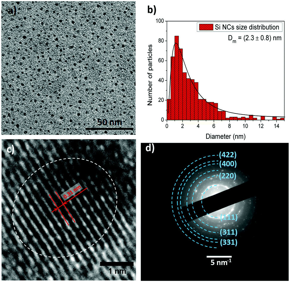 | ||
| Fig. 1 Transmission electron microscopy (TEM) characterization of the Si nanocrystals (NCs). (a) Low magnification TEM image, (b) size distribution with mean diameter (Dm), (c) high magnification TEM images and (d) diffraction pattern of the Si NCs. | ||
Fig. 2 shows the FTIR measurements of the Si NC thin films. The spectrum acquired for the Si NCs right after preparation (Fig. 2(a)) exhibits the typical characteristics of silicon NCs with absorption peaks related to the Si–Hx bonds.20 In particular, peaks at 626 cm−1, 862 cm−1, 902 cm−1 and 2130 cm−1 are associated with the Si–H stretching mode, Si–H3 symmetric deformation, Si–H2 scissor mode and Si–Hx stretch mode, respectively. A typical Si–O–Si absorption band is also observed at around 1075 cm−1,21 which suggests a very low degree of oxidation even after exposure to air, as this peak is generally prominent even with limited oxidation. Further confirmation of H-termination is obtained when analyzing the spectrum in the region between 2100 cm−1 and 2300 cm−1. The signal can be deconvoluted into three peaks, one at 2130 cm−1 corresponding to Si–Hx bonds as already mentioned, and another two at 2180 cm−1 and 2250 cm−1 which result from the insertion of oxygen into the Si–H back-bonds due to oxidation when the Si NCs are exposed to water vapor present in air.20 These last two peaks are not very noticeable in fresh Si NCs, supporting the formation of Si NCs with extensive hydrogen surface coverage.
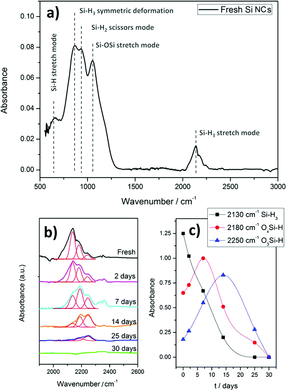 | ||
| Fig. 2 Fourier transform infra-red (FTIR) spectra of Si nanocrystals (NCs). (a) Fresh Si NCs; (b) and (c) deconvolution and integration of Si–H3 stretching mode peaks. | ||
An important aspect to be considered is therefore the oxidation of Si NCs over time when exposed to air. The oxidation process can be observed by deconvoluting and integrating specific FTIR peaks for different aging periods, as shown in Fig. 2(b) and (c). Fig. 2(c) in particular shows how the Si–H bond (with no back-bond oxidation) progressively decreases at the expense of the peaks representing back-bond oxidation, i.e. OxSi–H. The OxSi–H peaks initially increase as long as hydrogen terminations exist. Eventually these hydrogen terminations are fully replaced by an oxide layer. It is important to note that the oxidation process is in fact relatively slow, where back-bond oxidation reaches its maximum only after a few days. This may be justified by the size of the NCs which could slow down the oxidation process due to geometrical constraints.22 Also, it should be noted that Si–H bonds are very stable in dry air up to 500 °C,23 therefore the removal of the surface hydrogen, either from Si–H or from OxSi–H, is believed to occur only via the formation of Si–OH followed by condensation due to water vapor.22 Similar behavior was found for the other peaks related to Si–H bonds, resulting in an incremental increase in the peak intensity associated with Si–O–Si bonds (data not shown). Below we will consider freshly prepared Si NCs and therefore we will assume that these are H-terminated for the most part, with only negligible oxidation.
Absorption coefficient and direct/indirect bandgaps
Absorption and PL spectra of the atmospheric-pressure plasma synthesized Si NCs are shown in Fig. 3(a). The Si NCs exhibit continuous and relatively featureless absorption. The PL spectrum shows a peak close to the UV region, centered at 460 nm (2.69 eV). The PL signal does not present any shape alterations along the oxidation process that samples suffer when exposed to ambient air, but its intensity is reduced progressively.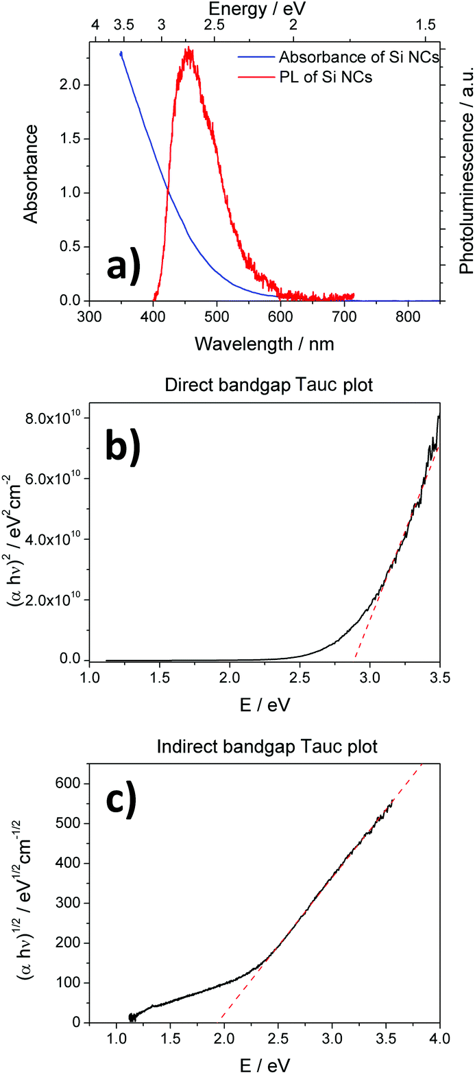 | ||
| Fig. 3 Optical characterization of the Si nanocrystals (NCs). (a) Ultra-violet visible absorbance spectrum of a Si NC thin film (blue line) and photoluminescence (PL) spectrum of the Si NCs. (b) Square and (c) square root of the absorption coefficient times the energy versus the energy. | ||
The absorbance measurements can be utilized first to determine the absorption coefficient and then to characterize the bandgap of Si NCs.24,25 The absorption coefficient of the Si NC thin film was calculated from absorption and thickness measurements (see ESI† for full calculation details), and the square and square root of the absorption coefficient times the energy are reported in Fig. 3(b) and (c), respectively. The direct bandgap (Edirect) can be estimated from the dependence of the absorption coefficient on the photon energy (hν). The square of the absorption coefficient is linearly dependent on hν at high photon energies (hν > Edirect). This can be seen from the graph in Fig. 3(b), which produces a direct bandgap of 2.87 eV. The indirect bandgap (Eindirect) is obtained from the linear dependence of the square root of the absorption coefficient on the photon energy below the direct bandgap (hν < Edirect), which produces a value of 1.92 eV. These values are consistent with the widening of the indirect bandgap (from the bulk value of 1.1 eV to 1.92 eV) and the reduction of the direct bandgap (from the bulk value of 3.3 eV to 2.87 eV) for quantum confined systems. Furthermore, this analysis reveals that the PL emission (Fig. 3(a)) originates from direct transitions. The relatively small Stoke's shift (∼0.16 eV) also supports this observation, suggesting that no surface effects are involved, i.e. the PL in Fig. 3(a) is due to core transitions. This is to be expected, as quantum confinement generally tends to take over surface effects when the electronegativity of the terminating element is lower than that of silicon.5,26 For instance, this is the case for hydrogen terminations where the low electronegative character of hydrogen limits the effect of surface transition dynamics and core-induced quantum confinement tends to dominate. Oxygen-based terminations on the other side have a strong influence on the optical transitions affecting the outcome of photoluminescence measurements, which often present large Stoke's shifts.
Energy band diagram
The Fermi level of Si NCs has been measured using a Kelvin probe system. This instrument provides the work function of the material in comparison with a known reference, gold in our case. According to Wandelt's local work function theory, the work function contains two contributions: the surface potential (inherent property of the material) and the surface dipole (dependent on the surface adsorption).27,28 In order to obtain a reliable estimation of the Fermi level, the second contribution must be minimized. In our case, this was achieved using a slightly p-type doped silicon wafer as the substrate and reference. The Si NCs were directly deposited on the substrate, forming a thin film with a thickness in the 1–2 μm range. Using this layer thickness we ensure that there is no contribution from the underlying silicon wafer during work function measurements. Fig. 4(a) shows the Fermi level measured for Si NCs in comparison with the bare silicon wafer. The value for the silicon wafer is very close to what was expected, at around −4.75 eV, while the Si NCs present a lower value close to −5.10 eV.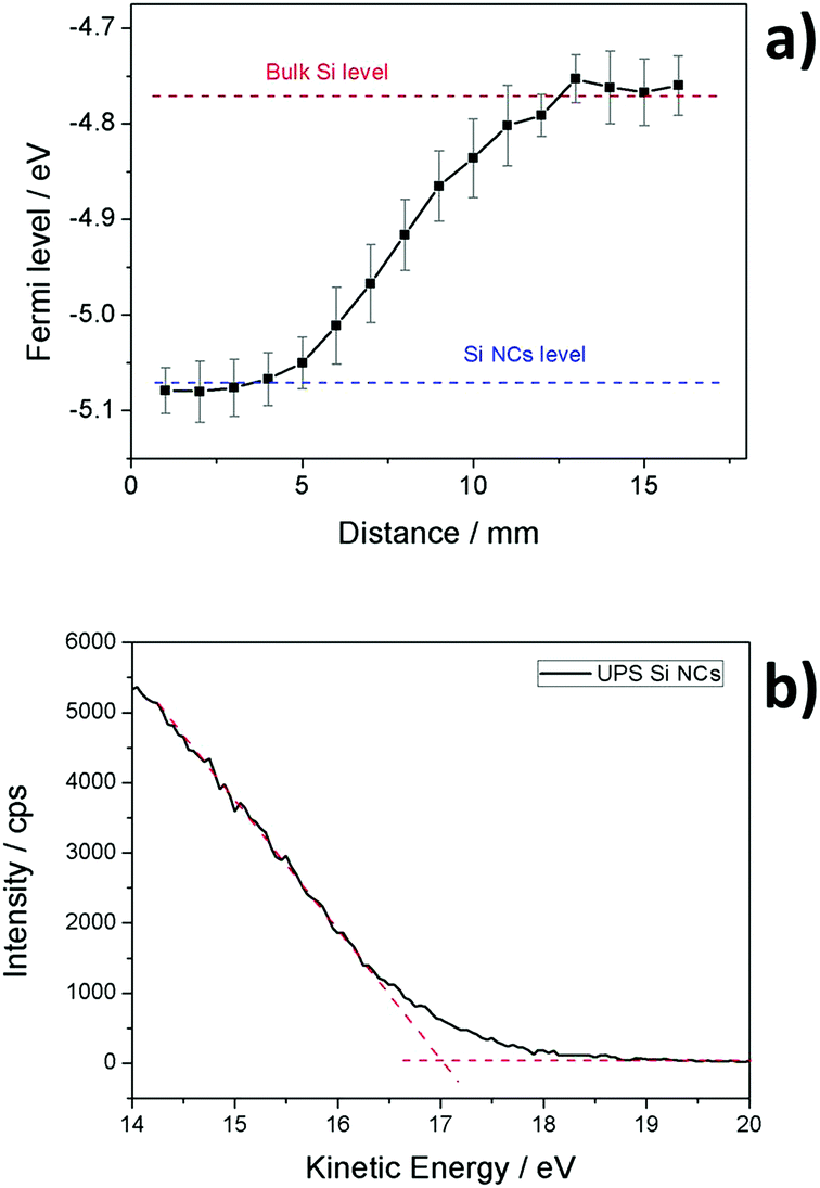 | ||
| Fig. 4 Fermi level and valence band measurements of the Si nanocrystals (NCs). (a) Fermi level extracted from work function measurements for the Si NCs in comparison with bulk silicon. (b) Ultraviolet Photoemission Spectroscopy (UPS) spectrum of the Si NCs at the valence band edge. | ||
The valence band edge level of the Si NCs was estimated using two different approaches: ultraviolet photoemission spectroscopy (UPS) and Mott–Schottky (MS) analysis. UPS measurements of the freshly prepared Si NCs are displayed in Fig. 4(b). Using the value of the absorption edge it is possible to calculate the valence band edge, which in the case of plasma-produced Si NCs is estimated to be −6.3 eV. In the case of the MS measurements, the flat-band potential can be estimated from the following MS relation:
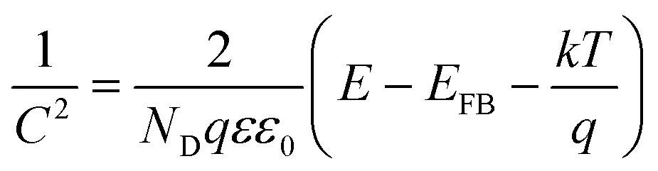 | (1) |
The flat-band potential calculated using MS analysis generally provides the value of the Fermi level of the film being analysed, however here it can be considered to be very close to the valence band-edge. This is because, while Kelvin probe and UPS are surface-sensitive techniques that essentially probe the Si NC surface, MS measurements rely on the formation of a depletion layer which is much larger than a few nanometers. It follows that the MS technique measures the flat-band potential of a highly hydrogenated nanocrystalline film, i.e. a heavily p-doped film where the Fermi level approaches the valence band-edge. While the single Si NCs are not expected to present defects within their cores (due to thermodynamic instability at these sizes), the strong p-type character of the film observed by MS measurements originates from the surfaces of the Si NCs. For instance, we can consider that with only one surface defect per NC, which is highly possible, we can achieve a high doping density. This would justify taking the flat-band potential to be a close estimate for the valence band-edge, possibly underestimating the absolute value. However, our results do show some differences in the valence band and highlight the need to develop accurate theories to extend the validity of these techniques to a range of nanoparticle systems.
We are now in the position to elucidate the energy band diagram of the Si NCs. On one hand, the bandgaps obtained from the optical characterization are 2.87 eV (direct) and 1.92 eV (indirect). On the other, MS and UPS measurements have provided the position of the valence band of the Si NCs. These values enable us to construct the full band energy diagram including the Fermi level produced by the Kelvin probe measurements. Fig. 5 presents the experimentally determined band energy diagram, featuring the valence and conduction bands together with the Fermi level that lies within both the direct and indirect bandgaps. In order to provide a context for these results, we have included in Fig. 5 theoretical calculations previously published by Ramos et al. and Kocevski et al. along with experimental bandgap values obtained by Furukawa et al. and Kortshagen et al.14,26,31,32 In these two latter cases, the band positions are located by adding one-third of the confinement energy to the position of the bulk silicon conduction band and subtracting two-thirds from the valence band. This method is based on density functional theory calculations that can have large errors.33
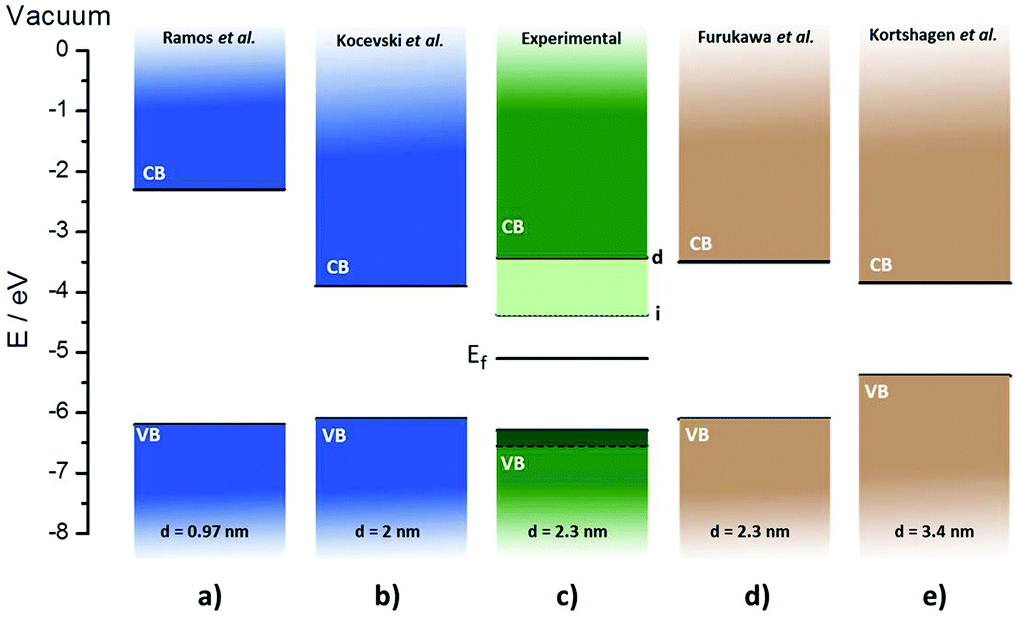 | ||
| Fig. 5 Energy bands diagrams of Si nanocrystals (NCs). (a) Ramos et al. theoretical calculations of Si nanocrystals (NCs) with 85 atoms,26 (b) Kocevski et al. theoretical calculations of 2 nm Si NCs,31 (c) present fully experimental measurements of 2.3 nm Si NCs, (d) and (e) Furukawa et al. and Kortshagen et al. experimental bandgap with theoretical assignment of band positions of Si NCs.14,32 | ||
Comparing the experimental energy diagram of the plasma-produced Si NCs with others of similar size (Fig. 5(b)–(d)), it is possible to observe that the experimentally obtained position of the bands matches fairly well with the previously reported references. Perhaps, the most significant difference appreciated is the lower position of the valence band registered experimentally, varying by 0.2 eV with respect to the same particle size references. The position of the valence band for larger particles (Fig. 5(e)) lies closer to bulk silicon, while models using a low number of atoms per particle (Fig. 5(a)) predict a lower position of the valence band, being closer to the experimental value obtained. Our results are however the first report of the band energy diagram determined fully from experimental measurements, therefore these results are of great interest since they join theoretical predictions with experimental data.
Conclusions
We have presented the synthesis of Si NCs using atmospheric pressure plasmas. The system presenting a novel configuration with two parallel flat electrodes produces high quality crystalline Si NCs. The versatility of the synthesis techniques has also allowed us to study the fundamental properties of the Si NCs. We have produced experimentally very important parameters that include the absorption coefficient, indirect/direct bandgap values, the Fermi level and the valence band-edge which have allowed the construction of the full energy band diagram for Si NCs for the first time. Furthermore, we have explored the use of a range of techniques and methodologies which are of great relevance for a wide range of nanoparticulated materials.Our work is of great relevance for a wide range of nanoscale and quantum confined systems and for their integration into device applications, e.g. for photovoltaics. Accurate and complementary experimental techniques are required together with appropriate theoretical models for a correct and full interpretation of results. Our results highlight that the determination of the energy structure for nanoscale systems is a topic that demands greater attention.
Acknowledgements
This work was supported by the EPSRC (EP/K022237/1) and the Leverhulme International Network (IN-2012-136). SA would like to acknowledge the support of the Ulster University Vice-Chancellor's Research Studentship and CR that of the NI-DEL studentship.References
- E. D. Sargent, Nat. Photonics, 2012, 6, 133 CrossRef CAS.
- Y. Shirasaki, G. J. Supran, M. G. Bawendi and V. Bulović, Nat. Photonics, 2013, 7, 13 CrossRef CAS.
- J. Fan and P. K. Chu, Small, 2010, 6, 2080 CrossRef CAS PubMed.
- D. K. Kim, Y. Lai, B. T. Diroll, C. B. Murray and C. R. Kagan, Nat. Commun., 2012, 3, 1216 CrossRef PubMed.
- D. Mariotti, S. Mitra and V. Švrček, Nanoscale, 2013, 5, 1385 RSC.
- V. Švrček, M. Kondo, K. Kalia and D. Mariotti, Chem. Phys. Lett., 2009, 478, 224 CrossRef.
- V. Švrček, D. Mariotti and M. Kondo, Appl. Phys. Lett., 2010, 97, 161502 CrossRef.
- R. J. Ellingson, M. C. Beard, J. C. Johnson, P. Yu, O. I. Micic, A. J. Nozik, A. Shabaev and A. L. Efros, Nano Lett., 2005, 5, 5 CrossRef PubMed.
- C. B. Murray, D. J. Noms and M. G. Bawendi, J. Am. Chem. Soc., 1993, 115, 19 Search PubMed.
- T. Makimura, T. Mizuta and K. Murakami, Jpn. J. Appl. Phys., 2002, 41, 144 Search PubMed.
- L. Xuegeng, H. Yuanqing, S. S. Talukdar and M. T. Swihart, Langmuir, 2003, 19, 8490 CrossRef.
- L. Mangolini, E. Thimsen and U. Kortshagen, Nano Lett., 2005, 5, 655 CrossRef CAS PubMed.
- K. Kůsová, O. Cibulka, K. Dohnalová, I. Pelant, J. Valenta, A. Fučíková, K. Žídek, J. Lang, J. Englich, P. Matějka, P. Štěpánek and S. Bakardjieva, ACS Nano, 2010, 4, 4495 CrossRef PubMed.
- A. M. P. Botas, R. A. S. Ferreira, R. N. Pereira, R. J. Anthony, T. Moura, D. J. Rowe and U. Kortshagen, J. Phys. Chem. C, 2014, 118, 10375 CAS.
- K. Hyeon-Deuk and O. V. Prezhdo, ACS Nano, 2012, 6, 1239 CrossRef CAS PubMed.
- D. Mariotti and R. M. Sankaran, J. Phys. D: Appl. Phys., 2011, 44, 174023 CrossRef.
- L. Mangolini, E. Thimsen and U. Kortshagen, Nano Lett., 2005, 5, 4 CrossRef PubMed.
- S. Askari, I. Levchenko, K. Ostrikov, P. Maguire and D. Mariotti, Appl. Phys. Lett., 2014, 104, 163103 CrossRef.
- W. Sun, C. Qian, L. Wang, M. Wei, M. L. Mastronardi, G. Casillas, J. Breu and G. A. Ozin, Adv. Mater., 2015, 27, 746 CrossRef CAS PubMed.
- D. Xu, L. Sun, H. Li, L. Zhang, G. Guo, X. Zhao and L. Gui, New J. Chem., 2003, 27, 300 RSC.
- G. Lucovsky, M. J. Manitini, J. K. Srivastava and E. A. Irene, J. Vac. Sci. Technol., B, 1987, 5, 530 CAS.
- D. Mariotti, V. Švrček, J. W. J. Hamilton, M. Schmidt and M. Kondo, Adv. Funct. Mater., 2012, 22, 954 CrossRef CAS.
- N. M. Johnson, C. E. Nebel, P. V. Santos, W. B. Jackson, R. A. Street, K. S. Stevens and J. Walker, Appl. Phys. Lett., 1991, 59, 1443 CrossRef CAS.
- J. Tauc, Mater. Res. Bull., 1968, 3, 37 CrossRef CAS.
- M. Kurosawa, M. Kato, T. Yamaha, N. Taoka, O. Nakatsuka and S. Zaima, Appl. Phys. Lett., 2015, 106, 171908 CrossRef.
- E. Ramos, B. M. Monroy, J. C. Alonso, L. E. Sansores, R. Salcedo and A. Martínez, J. Phys. Chem. C, 2012, 116, 3988 CAS.
- K. Wandelt, Appl. Surf. Sci., 1997, 1, 111 Search PubMed.
- Y. Song, L. Yan, Y. Zhou, B. Song and Y. Li, Adv. Mater. Interfaces, 2015, 2, 1400397 Search PubMed.
- K. Gelderman, L. Lee and S. W. Donne, J. Chem. Educ., 2007, 84, 685 CrossRef CAS.
- F. Cardon and W. P. Gomes, J. Phys. D: Appl. Phys., 1978, 11, L63 CrossRef CAS.
- V. Kocevski, O. Eriksson and J. Rusz, Phys. Rev. B: Condens. Matter, 2013, 87, 245401 CrossRef.
- S. Furukawa and T. Miyasato, Phys. Rev. B: Condens. Matter, 1988, 38, 5726 CrossRef CAS.
- T. Van Buuren, L. Dinh, L. Chase, W. Siekhaus and L. Terminello, Phys. Rev. Lett., 1998, 80, 3803 CrossRef CAS.
Footnote |
| † Electronic supplementary information (ESI) available. See DOI: 10.1039/c5nr07705b |
| This journal is © The Royal Society of Chemistry 2016 |