
 Open Access Article
 This Open Access Article is licensed under a Creative Commons Attribution-Non Commercial 3.0 Unported Licence
High-performance perovskite light-emitting diodes via morphological control of perovskite films†
Jae Choul
Yu‡
,
Da Bin
Kim‡
,
Eui Dae
Jung
,
Bo Ram
Lee
and
Myoung Hoon
Song
*
School of Materials Science Engineering/KIST-UNIST Ulsan Center for Convergent Materials, Ulsan National Institute of Science and Technology (UNIST), UNIST-gil 50, Ulsan, 689-798, Republic of Korea. E-mail: mhsong@unist.ac.kr
First published on 13th November 2015
Abstract
Solution-processable perovskite materials have garnered tremendous attention because of their excellent charge carrier mobility, possibility of a tunable optical bandgap, and high photoluminescence quantum efficiency (PLQE). In particular, the uniform morphology of a perovskite film is the most important factor in realizing perovskite light-emitting diodes (PeLEDs) with high efficiency and full-coverage electroluminescence (EL). In this study, we demonstrate highly efficient PeLEDs that contain a perovskite film with a uniform morphology by introducing HBr into the perovskite precursor. The introduction of HBr into the perovskite precursor results in a perovskite film with a uniform, continuous morphology because the HBr increases the solubility of the inorganic component in the perovskite precursor and reduces the crystallization rate of the perovskite film upon spin-coating. Moreover, PeLEDs fabricated using perovskite films with a uniform, continuous morphology, which were deposited using 6 vol% HBr in a dimethylformamide (DMF)/hydrobromic acid (HBr) cosolvent, exhibited full coverage of the green EL emission. Finally, the optimized PeLEDs fabricated with perovskite films deposited using the DMF/HBr cosolvent exhibited a maximum luminance of 3490 cd m−2 (at 4.3 V) and a luminous efficiency of 0.43 cd A−1 (at 4.3 V).
1. Introduction
Organic–inorganic hybrid semiconductors such as quantum dots and perovskite materials1–3 have attracted interest because of their excellent properties; these properties include superior charge carrier mobility compared to that of organic materials, a tunable optical bandgap, and easy solution processing, which raises the possibility of large-area displays and flexible device applications.4,5 Recently, solution-processable perovskite films with a photoluminescence quantum efficiency (PLQE) as high as 70% have been reported; the high PLQE of these films makes them promising semiconductor candidates for LED applications.6 Moreover, the perovskite materials used in solar cells have also demonstrated excellent photovoltaic (PV) performance, with efficiencies ranging from 4 to 19.3%.7,8The Cambridge group first reported green and infrared emissive perovskite light-emitting diodes (PeLEDs) whose bandgaps could be varied through changes in their chemical composition. These PeLEDs achieved a luminescence of 364 cd m−2 and a radiance of 6.8 W sr−1 m−2.3 Moreover, Kim et al. demonstrated highly efficient PeLEDs with a luminescence of 417 cd m−2 by modifying the workfunction of PEDOT:PSS using a self-organized buffer hole–injection layer (Buf-HIL), which reduced the hole–injection barrier between the PEDOT:PSS and the perovskite emissive layer.9 Recently, the Cambridge group also demonstrated a conventional structured PeLED fabricated using spatial atmospheric atomic layer-deposited (SAALD) Zn1−xMgxO as an electron transport layer (ETL).10 Their PeLED with an F8 layer exhibited a maximum luminescence efficiency of 364 cd m−2, whereas their PeLED with an SAALD layer exhibited a significantly improved maximum luminescence of 550 cd m−2 and enhanced air stability. One of the most important criteria for highly efficient perovskite optoelectronic devices is the uniform morphology of the perovskite crystal.11–14 However, previous papers regarding PeLEDs have not demonstrated a correlation between the perovskite morphology and the electroluminescence (EL) image in PeLEDs.
Here, we report the fabrication of a highly efficient perovskite-based green LED via the morphological control of methylammonium lead tribromide (CH3NH3PbBr3, MAPbBr3) films using a dimethylformamide (DMF)/hydrobromic acid (HBr) cosolvent through a 1-step spin-coat method. The optimized MAPbBr3-based PeLED fabricated using the DMF/HBr cosolvent method exhibited a maximum luminance of 3490 cd m−2 (at 4.3 V) and a maximum luminous efficiency of 0.43 cd A−1 (at 4.3 V). The high efficiency of the planar PeLED is due to both the uniform morphology of MAPbBr3 with full surface coverage and the optimized thicknesses of the MAPbBr3 and ETL polymer layers. The deposition of a uniform and dense MAPbBr3 layer with full surface coverage was achieved by adding an optimum amount of HBr to the perovskite precursor, and the full coverage of the green EL due to the highly uniform morphology of the perovskite layer was confirmed by optical microscopy.
2. Experimental
2.1 Materials
SPB-02 T polymer (product number: A.80827.0001) was purchased from Merck Co. and was used without purification. The CH3NH3Br synthesis and the preparation of the CH3NH3PbBr3 solution have been described elsewhere.152.2 Device fabrication
For the fabrication of PeLEDs (ITO/PEDOT:PSS/MAPbBr3/SPB-02 T/LiF/Ag), PEDOT:PSS was spin-coated onto a cleaned ITO/glass substrate at 5000 rpm for 45 s and subsequently annealed at 140 °C for 10 min. The MAPbBr3 precursor (37.8 wt% MABr and PbBr2 1![[thin space (1/6-em)]](https://www.rsc.org/images/entities/char_2009.gif) :1 molar ratio in N,N-dimethylformamide) solution with an aqueous HBr (48 wt%) solution in a volume ratio from 0 to 10 vol% were spin-coated onto the PEDOT:PSS-coated ITO/glass substrates at 3000 rpm for 60 s and annealed at 100 °C for 5 min under inert conditions. The electron transport layer was fabricated by coating SPB-02 T (blue copolymer) solution dispersed in chlorobenzene (0.45–0.72 wt%). Finally, LiF (1 nm) and silver (80 nm) were deposited by the vacuum thermal evaporation method using a 5-pixel mask. The active area of the device was 13.5 mm2. The devices were encapsulated and legged before testing.
:1 molar ratio in N,N-dimethylformamide) solution with an aqueous HBr (48 wt%) solution in a volume ratio from 0 to 10 vol% were spin-coated onto the PEDOT:PSS-coated ITO/glass substrates at 3000 rpm for 60 s and annealed at 100 °C for 5 min under inert conditions. The electron transport layer was fabricated by coating SPB-02 T (blue copolymer) solution dispersed in chlorobenzene (0.45–0.72 wt%). Finally, LiF (1 nm) and silver (80 nm) were deposited by the vacuum thermal evaporation method using a 5-pixel mask. The active area of the device was 13.5 mm2. The devices were encapsulated and legged before testing.
2.3 Characterization of MAPbBr3 films and PeLEDs
The PeLED measurements were performed using a Keithley 2400 source measurement unit and a Konica Minolta spectroradiometer (CS-2000, Minolta Co.).15 Scanning electron microscopy (Nanonova 230, FEI) was used to observe the morphology of the MAPbBr3 films. XRD patterns were obtained from the samples of MAPbBr3 with the HBr (0–10 vol%) cosolvent deposited onto the PEDOT:PSS substrate; the patterns were recorded using an X-ray diffractometer (D8 Advance, Bruker) equipped with a Cu-Kα radiation source (λ = 1.5405 Å). A step size of 0.01° was chosen with an acquisition time as high as 5 min deg−1. EL microscopy images were obtained from the samples of PeLEDs using an optical microscope (IX81, Olympus).3. Results and discussion
3.1 Device structure
Fig. 1(a) shows a schematic of the device structure (ITO/PEDOT:PSS/MAPbBr3/SPB-02 T/LiF/Ag) used in the PeLED, and Fig. 1(b) shows a cross-sectional image of the complete PeLED, which is composed of indium tin oxide (ITO) as the anode, PEDOT:PSS as the transport layer (HTL), MAPbBr3 with the DMF/HBr cosolvent as the perovskite emissive layer, SPB-02 T (blue copolymer, Merck Co.) as the ETL, and LiF/Al as the cathode. Fig. S1† shows the energy-level diagram of the fabricated PeLED. SPB-02 T is a commercial material, the material information including the structure and the energy level unfortunately is unknown. Thus, the energy level of SPB-02 T was inferred from that of the SPW-111 co-polymer (Merck Co.) with a similar structure.16 The fabrication of the PeLEDs with the DMF/HBr cosolvent is described in detail in the Experimental section.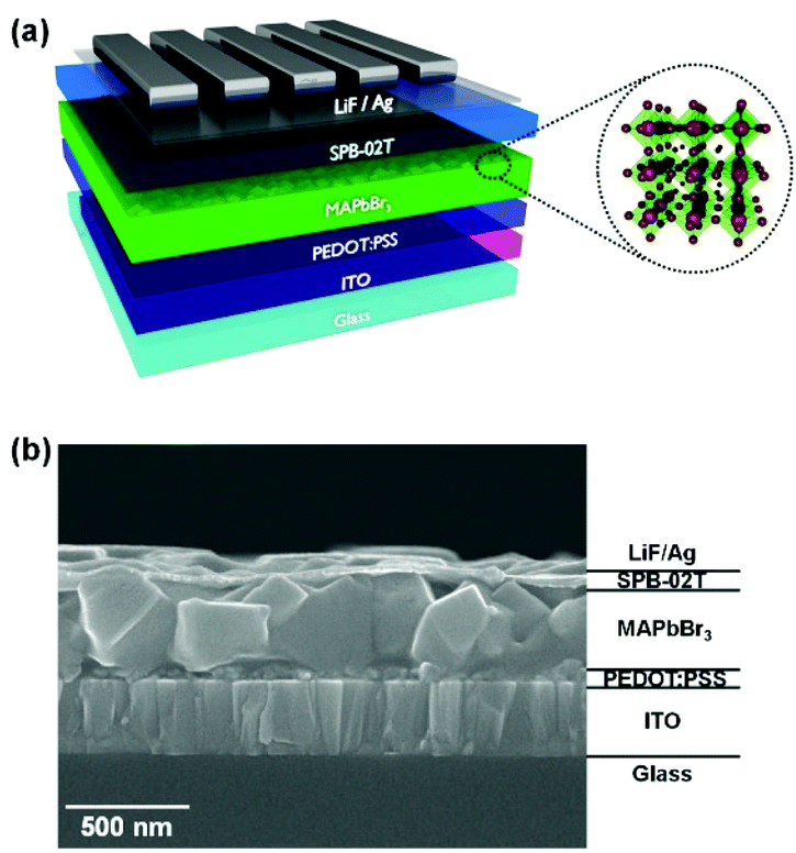 | ||
| Fig. 1 (a) Schematic of the PeLED device with a fully coated perovskite layer. (b) Scanning electron micrograph cross-sectional image of the complete device with a perovskite layer prepared using 6 vol% of HBr in the DMF/HBr cosolvent. | ||
3.2 Viscosity measurement
Morphological control of perovskite films is important in improving device performance.15 Thus, slow crystallization rates lead to the formation of a thinner perovskite film with full surface coverage because of the retarded nucleation time. The addition of an acid in the perovskite precursor solution is well known to slow the crystallization rate and improve the solubility of the solution through the enhanced solubility of the inorganic component.17,18 Thus, HBr was added to the MAPbBr3 precursor solution to obtain a MAPbBr3 film with full surface coverage. In addition, the viscosity was measured to support the slow crystallization rate, which increased linearly with increasing HBr concentration, as shown in Fig. S2.† As a result, the crystallization rate of the perovskite film was reduced upon spin-coating; thus, a dense MAPbBr3 film with greater surface coverage was fabricated on a PEDOT:PSS-coated ITO/glass substrate.3.3 Scanning electron microscopy
To confirm the dense and full coverage of the MAPbBr3 film, the morphology of the MAPbBr3 films, which were deposited on PEDOT:PSS-coated ITO/glass substrates by spin-coating using different concentrations of HBr (0–10 vol%) in the DMF/HBr cosolvent, was observed using a scanning electron microscope (SEM); the resulting micrographs are shown in Fig. 2. The MAPbBr3 films prepared using 0–4 vol% of HBr in the DMF/HBr cosolvent appeared to partially cover the substrate with islands and voids with submicron distances between them, as shown in Fig. 2(a)–(c). In contrast, the MAPbBr3 film prepared using 6 vol% of HBr in the DMF/HBr cosolvent exhibited full coverage and a much smoother surface. However, the MAPbBr3 film surfaces prepared using 8–10 vol% of HBr in the DMF/HBr cosolvent exhibited unwanted cube-shaped crystals on top of the MAPbBr3 films, as shown in Fig. 2(e) and (f). The reason for the formation of these unwanted crystals may be the growth of larger MAPbBr3 crystals at the expense of smaller MAPbBr3 crystals because of their reduced surface energy. In fact, this phenomenon of crystal growth is well-known as Ostwald ripening and can be easily observed in the case of quantum dots.19,20 In addition, the thickness of the MAPbBr3 film decreased as the concentration of HBr in the DMF/HBr cosolvent increased, as shown in Fig. S2.† As previously mentioned, a greater viscosity yields a thinner MAPbBr3 layer because of the retarded evaporation rate of the solvent; as a result, the crystallization rate will be delayed. As the concentration of HBr in the DMF/HBr cosolvent was increased to 8–10 vol%, unwanted cube-shaped crystals were created; consequently, the overall thickness and roughness increased due to Ostwald ripening. Therefore, the concentration of HBr in the DMF/HBr cosolvent used to spin-coat MAPbBr3 was confirmed to strongly influence the final film morphology and thickness of the MAPbBr3 layers.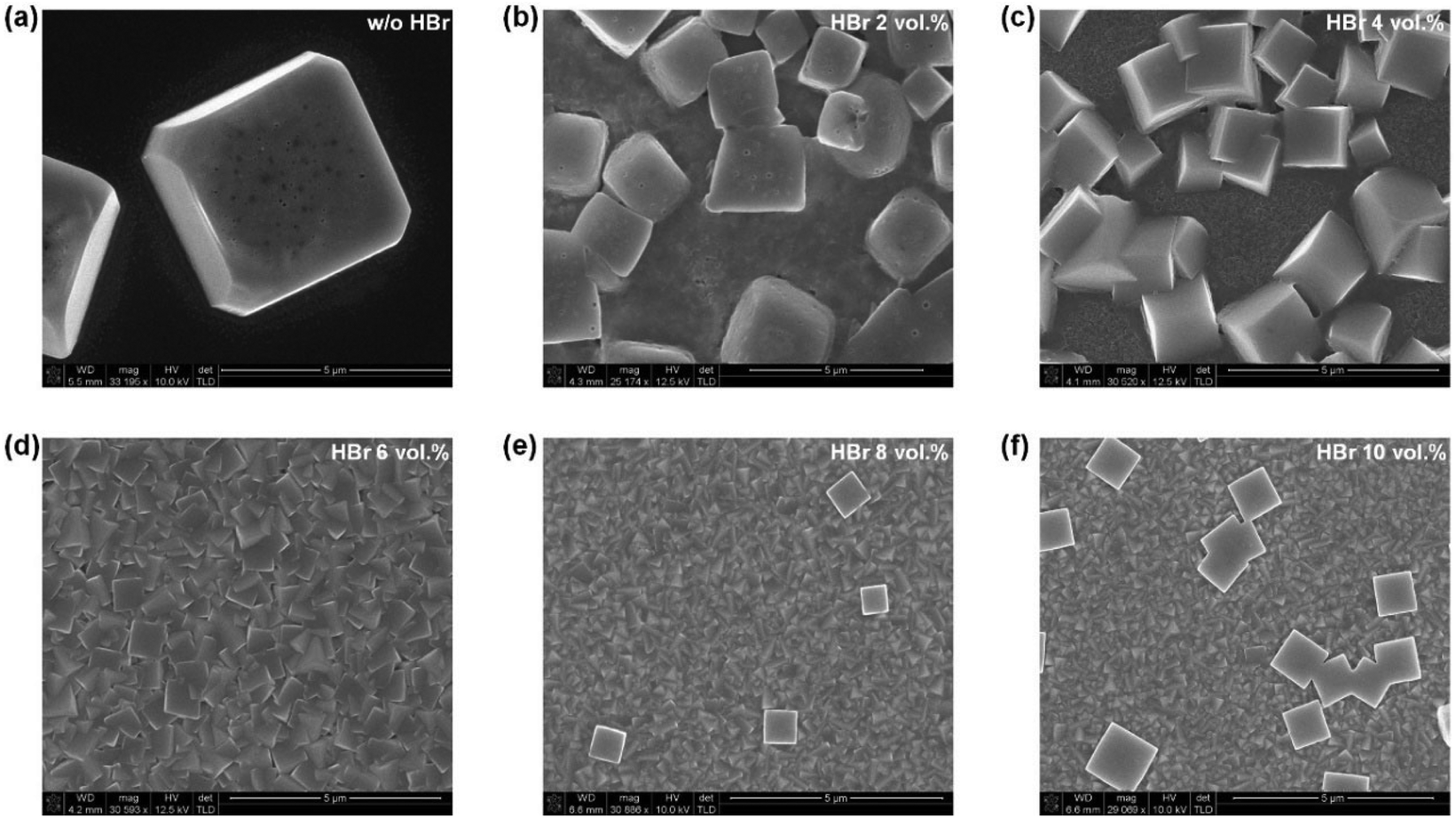 | ||
| Fig. 2 SEM images of the top surfaces of the MAPbBr3 layers deposited using 0–10 vol% of HBr in the DMF/HBr cosolvent on PEDOT:PSS-coated ITO/glass substrates. | ||
To observe other factors that affect the crystallization process, MAPbBr3 films with different annealing times and different spin-speeds used to spin-coat the MAPbBr3 precursor solution using 6 vol% of HBr in the DMF/HBr cosolvent were prepared and their SEM images were compared. The MAPbBr3 films maintained their original morphology, and the Ostwald ripening phenomenon was not observed in the top-view SEM images in Fig. S4 and S5,† despite the annealing time and spin-coating speeds being different. Moreover, the crystal size decreased from 1.5 μm to 500 nm, and the film thickness of an MAPbBr3 single layer with 6 vol% of HBr in the DMF/HBr cosolvent decreased when the spin-coating speed was increased from 1000 rpm to 7000 rpm (Fig. S6†). These results demonstrate that the main factor that influences the morphology of the MAPbBr3 films is the concentration of HBr in the DMF/HBr cosolvent. This simple technique should prove extremely useful as a general method to control the MAPbBr3 crystal size and film thickness with full surface coverage.
3.4 Optical microscopy
Fig. 3(a)–(e) show the EL images of complete PeLED devices with MAPbBr3 films prepared at a constant voltage using different concentrations of HBr in the DMF/HBr cosolvent; a significant correlation between the morphology of the MAPbBr3 films and the EL behavior of complete PeLEDs was observed in the optical microscopy images. The PeLED devices with an inhomogeneous surface of the MAPbBr3 films with an island-like morphology (0–4 vol% of HBr in the DMF/HBr cosolvent) showed island-like emission (Fig. 3(a)–(c)), whereas the PeLED device with a homogeneous surface of the MAPbBr3 films (6 vol% of HBr in the DMF/HBr cosolvent) showed full coverage of the green emission through the full coverage of the uniform MAPbBr3 film (Fig. 3(d)). However, the PeLED device with MAPbBr3 films deposited using 8 vol% of HBr in the DMF/HBr cosolvent showed minimum island-like light emission even at a higher applied voltage of 5.4 V in Fig. 3(e) because unwanted MAPbBr3 parts were fabricated on top of the thinner MAPbBr3 layer in Fig. S3(e).†Fig. 3(f) and (g) present images of 1 cm2 emission areas from the MAPbBr3-based PeLED devices without and with using 6 vol% of HBr in the DMF/HBr cosolvent at 3.3 V and 3.1 V biases, respectively; the MAPbBr3-based PeLED prepared using 6 vol% of HBr in the DMF/HBr cosolvent exhibited brighter and more uniform green emission than that without using 6 vol% of HBr in the DMF/HBr cosolvent.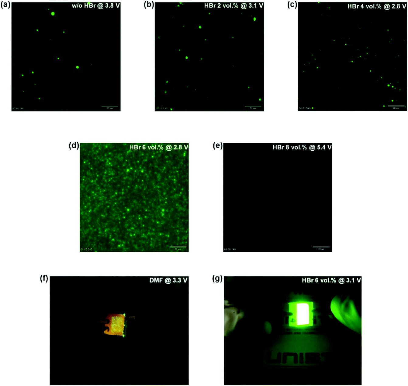 | ||
| Fig. 3 (a–e) Optical microscopy images of EL from PeLEDs with the MAPbBr3 layers deposited at a constant voltage using different concentrations of HBr in the DMF/HBr cosolvent. (f and g) 1 cm2-area green EL from MAPbBr3 PeLEDs without and with 6 vol% of HBr in the DMF/HBr cosolvent, respectively. | ||
3.5 X-ray diffraction
To confirm the unwanted layer of MAPbBr3 when 8–10 vol% of HBr was used in the DMF/HBr cosolvent, as previously mentioned, the XRD patterns of the resulting films were collected, as shown in Fig. 4(a). The PbBr2 peak and MAPbBr3 peak coexisted in the pattern of the MAPbBr3 film when HBr was not added to the DMF/HBr cosolvent, whereas the intensity of the PbBr2 peak decreased upon the addition of HBr and almost disappeared when the DMF/HBr cosolvent contained 6 vol% of HBr, which is the similar result to previous literature.18 However, the PbBr2 peak was clearly observed in the pattern of MAPbBr3 films when the DMF/HBr cosolvent contained 8–10 vol% of HBr; these peaks were a consequence of the unwanted MAPbBr3 crystals that resulted from Ostwald ripening during the film growth of the MAPbBr3 layers. The remnant PbBr2 acts as a defect site in perovskite, resulting in an increased rate of non-radiative recombintation and reduced device performance.21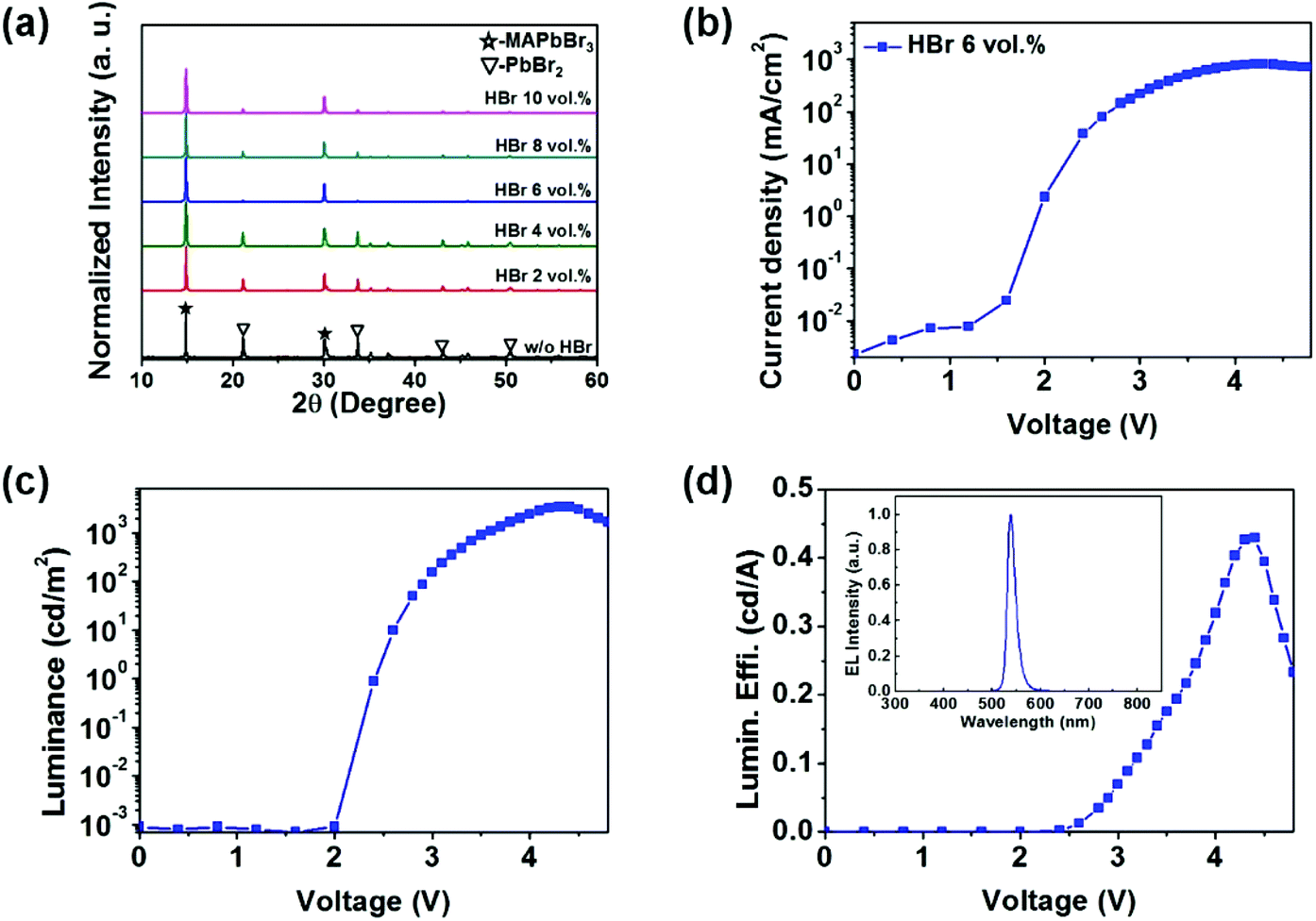 | ||
| Fig. 4 (a) XRD data of MAPbBr3 films with different volume ratios of HBr in the DMF/HBr cosolvent, where the MAPbBr3 films were deposited onto PEDOT:PSS-coated ITO/glass substrates. Light-emitting characteristics of PeLEDs (ITO/PEDOT:PSS/MAPbBr3 (400 nm)/SPB-02 T(30 nm)/LiF (1 nm)/Ag (80 nm)) with MAPbBr3 prepared using 6 vol% of HBr in the DMF/HBr cosolvent are presented in terms of (b) current density vs. the applied voltage (J–V), (c) luminance vs. the applied voltage (L–V), and (d) luminous efficiency vs. the applied voltage (LE–V). The inset shows the EL spectrum (530 nm) from the tested PeLEDs. | ||
3.6 Device performance
The voids and pinholes of the MAPbBr3 film create shunt pathways between the HTL and the ETL, which limits the device performance.22 As the voltage bias increases, such pinholes would cause dielectric breakdown; thus, the devices with the non-optimized MAPbBr3 layers were observed to easily short-circuit. Fig. S7† shows (a) the current–density vs. voltage (J–V), (b) the luminance vs. voltage (L–V), and (c) the luminous efficiency vs. voltage (LE–V) characteristics and (d) electroluminescence (EL) spectra of PeLEDs with the MAPbBr3 layers deposited using different concentrations of HBr in the DMF/HBr cosolvent. As the concentration of HBr increased up to 6 vol% in the DMF/HBr cosolvent, the current densities were reduced and the luminance values were enhanced due to the formation of uniform and thinner MAPbBr3 films. On the other hand, the current density and the luminance value of the PeLED using 8 vol% of HBr in the DMF/HBr cosolvent dramatically decreased and both 480 nm and 540 nm emission spectra from SPB-02 T and MAPbBr3 were observed due to the creation of unwanted and nonuniform MAPbBr3 layers. The detailed device performances of the PeLEDs are summarized in Table S1.† Next, the PeLEDs with the uniform morphology of MAPbBr3 prepared using 6 vol% of HBr in the DMF/HBr cosolvent were fabricated and measured by changing the spin speed to control the MAPbBr3 films and the thickness of the ETL layer. Fig. 4 shows (b) J–V, (c) L–V, and (d) the external quantum efficiency vs. voltage (EQE–V) characteristics of the optimized MAPbBr3-based PeLED prepared using 6 vol% of HBr in the DMF/HBr cosolvent. The inset image shows the EL spectra of the MAPbBr3 PeLED. The PeLED with the MAPbBr3 deposited using 6 vol% of HBr in the DMF/HBr cosolvent exhibited a maximum luminance of 3490 cd m−2 (at 4.3 V) and a luminous efficiency of 0.43 cd A−1 (at 4.3 V). The detailed device performance of the optimized MAPbBr3-based PeLED prepared using 6 vol% of HBr in the DMF/HBr cosolvent is summarized in Table 1. It should be noted that the maximum luminance value of our inverted PeLED is the highest value so far presented for inverted structure PeLED devices with MAPbBr3 layers deposited onto PEDOT:PSS coated ITO substrates (Table S2†).| Device configuration | L max[cd m−2]@bias | LEmax[cd A−1]@bias | PEmax[lm W−1]@bias | EQEmax[%]@bias |
|---|---|---|---|---|
| ITO/PEDOT:PSS/MAPbBr3 (HBr 6 vol% in the DMF/HBr cosolvent)/SPB-02 T/LiF/Ag | 3490@4.3 | 0.43@4.3 | 0.31@4.3 | 0.10@4.3 |
The multilayered structure of polymer LEDs can be challenging to fabricate by a solution process because of the non-orthogonal nature of the solvents used to deposit subsequent layers. In contrast, the multilayered structure of a PeLED with MAPbBr3 and emissive ETL polymers fabricated via a solution process can be easily fabricated because the solvents used to deposit the MAPbBr3 (DMF/HBr) and SPB-02 T layers (chlorobenzene) are orthogonal. Such hybrid devices have the advantage of a broad emission, as demonstrated in nanocrystal–polymer hybrid LEDs by changing the thickness of the polymer or the nanocrystal.23,24 PeLED devices (ITO/PEDOT:PSS/MAPbBr3 (250–800 nm)/SPB-02 T (55 nm)/LiF/Ag) with different thicknesses of MAPbBr3 were fabricated, as shown in Fig. S7(a).† Two mixed EL emissions from MAPbBr3 and SPB-02 T observed in the PeLEDs with less than 400 nm-thick MAPbBr3 layers. As the thickness of the MAPbBr3 layers was increased in PeLEDs with a fixed thickness of SPB-02 T (55 nm), the EL spectra from SPB-02 T disappeared, and the 540 nm EL spectra for the PeLEDs with a MAPbBr3 thickness between 400 and 800 nm appeared dominant because of the shift of the recombination by charge carriers. Moreover, both 480 nm and 540 nm emission spectra were observed as the thickness of the SPB-02 T layer was increased in the PeLED (ITO/PEDOT:PSS/MAPbBr3 (280 nm)/SPB-02 T (15–55 nm)/LiF/Ag), as shown in Fig. S8(b).† Thus, different colors of the EL emission were realized by controlling the recombination zone, which tuned the thicknesses of the MAPbBr3 and SPB-02 T layers in the organic–inorganic hybrid PeLEDs. Fig. S9† shows the EL spectra of two PeLEDs with different thickness sets of MAPbBr3 and SPB-02 T layers under applied voltages. The clear single mode emission (λmax = 540 nm) with narrow full width half maximum (FWHM) was observed in our optimized PeLED (ITO/PEDOT:PSS/MAPbBr3 (400 nm)/SPB-02 T (30 nm)/LiF/Ag) and it didn't change under applied voltages, which represents that the recombination occurs within the MAPbBr3 layer. Whereas the two mixed emissions of the PeLED (ITO/PEDOT:PSS/MAPbBr3 (280 nm)/SPB-02 T (55 nm)/LiF/Ag) were observed and they changed under applied voltages. The change of the emission under applied voltages indicates that the electron–hole recombination zone in the PeLED (ITO/PEDOT:PSS/green emissive MAPbBr3 (280 nm)/blue emissive SPB-02 T (55 nm)/LiF/Ag) is close to the MAPbBr3/SPB-02 T interface and change spatially with the applied electric field. These results are in agreement with the behavior of emission reported in the literature.25,26
It is noted that SPB-02 T is certainly not the best candidate for an ETL because the emission spectrum of SPB-02 T has overlapped with the absorption spectrum of MAPbBr3. To confirm whether the energy transfer between the MAPbBr3 emissive layer and SPB-02 T occurs or not, we used the same thickness condition of Fig. 4(b) (ITO/PEDOT:PSS/MAPbBr3 (400 nm)/SPB-02 T (Merck Co., 30 nm)/LiF/Ag), but replaced the blue-emissive SPB-02 T with green-emissive super yellow (SY, Merck Co., 30 nm) to avoid overlap of the absorption spectrum of MAPbBr3 and the emission spectrum of SY, as shown in Fig. S10.† It is assumed that the electron mobility of SPB-02 T and SY is almost the same because they are fabricated from Merck Co. and have a similar back-bone. The emission spectrum from the PeLED (ITO/PEDOT:PSS/MAPbBr3 (400 nm)/SY (30 nm)/LiF/Ag) is narrow and is the same as that from PeLED (ITO/PEDOT:PSS/MAPbBr3 (400 nm)/SPB-02 T (30 nm)/LiF/Ag)3 in Fig. S10(d),† which represents that the recombination occurs within the MAPbBr3 layer and SPB-02 T acts only as an ETL and does not participate in light emission. Moreover, device performances of two PeLEDs were compared and the luminance and efficiency values of two PeLEDs were almost the same in Fig. S10 and Table S3.† This result clearly supports that a similar device performance is obtained by using polymers with a similar back-bone and electron mobility as an ETL in the PeLEDs of Fig. S10.†
4. Conclusions
In summary, we successfully fabricated highly efficient PeLEDs via a uniform and dense MAPbBr3 film with full surface coverage on a PEDOT:PSS-coated ITO/glass substrate by using the optimal concentration of HBr in the DMF/HBr solution. The PeLED with 6 vol% of HBr in the DMF/HBr cosolvent exhibited a maximum luminance of 3490 cd m−2 (at 4.3 V) and maximum luminous efficiency levels as high as 0.43 cd A−1 (at 4.3 V). The addition of a small amount of HBr to the DMF solvent enables the formation of a dense and uniform MAPbBr3 film with full surface coverage, which facilitates full-coverage EL emission of the fabricated PeLED, resulting in a highly efficient PeLED. By incorporating an electron-transport layer that is itself a luminescent conjugated polymer, uniform green emission from the MAPbBr3/polymer-based PeLED was realized by controlling the recombination region between the MAPbBr3 layer and the luminescent polymer layer by changing the thickness of the SPB-02 T layer used as the ETL. In addition, the EL emission spectra of the MAPbBr3/polymer-based PeLEDs were tuned by controlling the thickness of the perovskite and polymer layers. This approach provides a powerful tool to understand the electroluminescence recombination zone from the emission spectra and a potentially useful approach to apply to broad-band LEDs. Moreover, the prospect of optimizing the processing of perovskite crystallization and the availability of a variety of light-emitting polymers provide a promising future for tailor-made, efficient PeLEDs with desired emission profiles.Acknowledgements
This study was supported by the Mid-Career Researcher Program (2015R1A2A2A01003263). This work was financially supported by the KIST-UNIST partnership program (1.150091.01/2.150464.01). This work was supported by the Human Resource Training Program for Regional Innovation and Creativity through the Ministry of Education and National Research Foundation of Korea (NRF-2014H1C1A1073051).Notes and references
- J. H. Burroughes, D. D. C. Bradley, A. R. Brown, R. N. Marks, K. Mackay, R. H. Friend, P. L. Burns and A. B. Holmes, Nature, 1990, 347, 539 CrossRef CAS.
- V. L. Colvin, M. C. Schlamp and A. P. Alivisatos, Nature, 1994, 370, 354 CrossRef CAS.
- Z. K. Tan, R. S. Moghaddam, M. L. Lai, P. Docampo, R. Higler, F. Deschler, M. Price, A. Sadhanala, L. M. Pazos, D. Credgington, F. Hanusch, T. Bein, H. J. Snaith and R. H. Friend, Nat. Nanotechnol., 2014, 9, 687 CrossRef CAS PubMed.
- G. Gustafsson, Y. Cao, G. M. Treacy, F. Klavetter, N. Colaneri and A. J. Heeger, Nature, 1992, 357, 477 CrossRef CAS.
- K. G. Lim, H. B. Kim, J. Jeong, H. Kim, J. Y. Kim and T. W. Lee, Adv. Mater., 2014, 26, 6461 CrossRef CAS PubMed.
- F. Deschler, M. Price, S. Pathak, L. E. Klintberg, D. D. Jarausch, R. Higler, S. Huttner, T. Leijtens, S. D. Stranks, H. J. Snaith, M. Atature, R. T. Phillips and R. H. Friend, J. Phys. Chem. Lett., 2014, 5, 1421 CrossRef CAS PubMed.
- A. Kojima, K. Teshima, Y. Shirai and T. Miyasaka, J. Am. Chem. Soc., 2009, 131, 6050 CrossRef CAS PubMed.
- H. Zhou, Q. Chen, G. Li, S. Luo, T. B. Song, H. S. Duan, Z. Hong, J. You, Y. Liu and Y. Yang, Science, 2014, 345, 542 CrossRef CAS PubMed.
- Y. H. Kim, H. Cho, J. H. Heo, T. S. Kim, N. Myoung, C. L. Lee, S. H. Im and T. W. Lee, Adv. Mater., 2015, 27, 1248 CrossRef CAS PubMed.
- R. L. Hoye, M. R. Chua, K. P. Musselman, G. Li, M. L. Lai, Z. K. Tan, N. C. Greenham, J. L. MacManus-Driscoll, R. H. Friend and D. Credgington, Adv. Mater., 2015, 27, 1414 CrossRef CAS PubMed.
- M. Liu, M. B. Johnston and H. J. Snaith, Nature, 2013, 501, 395 CrossRef CAS PubMed.
- J. Burschka, N. Pellet, S. J. Moon, R. Humphry-Baker, P. Gao, M. K. Nazeeruddin and M. Gratzel, Nature, 2013, 499, 316 CrossRef CAS PubMed.
- G. E. Eperon, V. M. Burlakov, P. Docampo, A. Goriely and H. J. Snaith, Adv. Funct. Mater., 2014, 24, 151 CrossRef CAS.
- N. K. Kumawat, A. Dey, K. L. Narasimhan and D. Kabra, ACS Photonics, 2015, 2, 349 CrossRef CAS.
- J. C. Yu, D. B. Kim, G. Baek, B. R. Lee, E. D. Jung, S. Lee, J. H. Chu, K. J. Choi, S. Cho and M. H. Song, Adv. Mater., 2015, 27, 3492 CrossRef CAS PubMed.
- M. A. M. Sarjidan, H. A. M. Mokhtar and W. H. A. Majid, J. Lumin., 2015, 159, 134 CrossRef.
- G. E. Eperon, S. D. Stranks, C. Menelaou, M. B. Johnston, L. M. Herz and H. J. Snaith, Energy Environ. Sci., 2014, 7, 982 CAS.
- J. H. Heo, D. H. Song and S. H. Im, Adv. Mater., 2014, 26, 8179 CrossRef CAS PubMed.
- R. D. Vengrenovich, Y. V. Gudyma and S. V. Yarema, Semiconductors, 2001, 35, 1378 CrossRef CAS.
- W. C. Chan, D. J. Maxwell, X. Gao, R. E. Bailey, M. Han and S. Nie, Curr. Opin. Biotechnol., 2002, 13, 40 CrossRef CAS PubMed.
- J. H. Heo, H. J. Han, D. Kim, T. K. Ahn and S. H. Im, Energy Environ. Sci., 2015, 8, 1602 CAS.
- W. Zhang, M. Saliba, D. T. Moore, S. K. Pathak, M. T. Horantner, T. Stergiopoulos, S. D. Stranks, G. E. Eperon, J. A. Alexander-Webber, A. Abate, A. Sadhanala, S. Yao, Y. Chen, R. H. Friend, L. A. Estroff, U. Wiesner and H. J. Snaith, Nat. Commun., 2015, 6, 6142 CrossRef CAS PubMed.
- S. Coe, W. K. Woo, M. Bawendi and V. Bulovic, Nature, 2002, 420, 800 CrossRef CAS PubMed.
- N. Tessler, V. Medvedev, M. Kazes, S. Kan and U. Banin, Science, 2002, 295, 1506 CrossRef PubMed.
- A. Sadhanala, A. Kumar, S. Pathak, A. Rao, U. Steiner, N. C. Greenham, H. J. Snaith and R. H. Friend, Adv. Electron. Mater., 2015, 1, 1500008 Search PubMed.
- J. Zaumseil, R. H. Friend and H. Sirringhaus, Nat. Mater., 2006, 5, 69 CrossRef CAS.
Footnotes |
| † Electronic supplementary information (ESI) available: Viscosity, top view and cross-sectional SEM images of the MAPbBr3 film, energy diagram and device characteristics of PeLEDs. See DOI: 10.1039/c5nr05604g |
| ‡ These authors contributed equally. |
| This journal is © The Royal Society of Chemistry 2016 |