
 Open Access Article
 This Open Access Article is licensed under a
 Creative Commons Attribution 3.0 Unported Licence
Electrochemically synthesized amorphous and crystalline nanowires: dissimilar nanomechanical behavior in comparison with homologous flat films†
M. A.
Zeeshan‡
a,
D.
Esqué-de los Ojos‡
b,
P.
Castro-Hartmann
c,
M.
Guerrero
b,
J.
Nogués
d,
S.
Suriñach
b,
M. D.
Baró
b,
B. J.
Nelson
a,
S.
Pané
*a,
E.
Pellicer
*b and
J.
Sort
*e
aInstitute of Robotics and Intelligent Systems (IRIS), ETH Zürich, CH-8092 Zürich, Switzerland. E-mail: vidalp@ethz.ch
bDepartament de Física, Facultat de Ciències, Universitat Autònoma de Barcelona, E-08193 Bellaterra, Spain. E-mail: eva.pellicer@uab.cat
cServei de Microscòpia, Facultat de Ciències, Universitat Autònoma de Barcelona, E-08193 Bellaterra, Spain
dInstitució Catalana de Recerca i Estudis Avançats (ICREA) and ICN2 – Institut Catala de Nanociencia i Nanotecnologia, Campus UAB, 08193 Bellaterra (Barcelona), Spain
eInstitució Catalana de Recerca i Estudis Avançats (ICREA) and Departament de Física, Universitat Autònoma de Barcelona, E-08193 Bellaterra, Spain. E-mail: jordi.sort@uab.cat
First published on 8th September 2015
Abstract
The effects of constrained sample dimensions on the mechanical behavior of crystalline materials have been extensively investigated. However, there is no clear understanding of these effects in nano-sized amorphous samples. Herein, nanoindentation together with finite element simulations are used to compare the properties of crystalline and glassy CoNi(Re)P electrodeposited nanowires (ϕ ≈ 100 nm) with films (3 μm thick) of analogous composition and structure. The results reveal that amorphous nanowires exhibit a larger hardness, lower Young's modulus and higher plasticity index than glassy films. Conversely, the very large hardness and higher Young's modulus of crystalline nanowires are accompanied by a decrease in plasticity with respect to the homologous crystalline films. Remarkably, proper interpretation of the mechanical properties of the nanowires requires taking the curved geometry of the indented surface and sink-in effects into account. These findings are of high relevance for optimizing the performance of new, mechanically-robust, nanoscale materials for increasingly complex miniaturized devices.
1. Introduction
The rapid progress in different fields of nanotechnology has prompted an unprecedented revolution in the methods to synthesize materials with nanoscale lateral dimensions and the procedures to assemble them into miniaturized devices. When the size of a given object is reduced to the sub-micrometer range, many of its properties become radically different from bulk properties. From a mechanical viewpoint, the size effects manifest in variations of hardness, H, Young's modulus, E, or plasticity.1 In nano-sized crystalline materials an increase of the yield stress occurs as a result of lateral confinement and the need to create the so-called “geometrically-necessary dislocations” in order to accommodate the imposed shear strain.2–4 Conversely, the reduction of lateral size is usually detrimental in terms of ductility, since dislocations have difficulties nucleating and gliding in small crystals.Because of the lack of a crystallographic structure, amorphous metallic alloys do not deform via propagation of dislocations. Instead, plastic flow in these materials is accompanied by the net creation of free volume.5,6 The excess free volume tends to coalesce into shear bands, leading to inhomogeneous plastic flow and premature fracture.6,7 It has been suggested that this embrittlement becomes less significant if the sample is smaller than the “process zone size”, i.e. the critical size of the plastic zone at the tip of a sharp crack, typically of the order of a few μm.7 For extremely small (sub-200 nm) samples, embryonic shear bands cannot fully develop and homogeneous deformation occurs.8–11
The effect of constrained sample dimensions on H and E in amorphous alloys remains controversial. While some researchers have shown that the trend “smaller is stronger” for crystalline materials remains valid for metallic glasses,10,12 others have reported the opposite.9,13,14 It has also been proposed that the yield stress in amorphous alloys can be size-independent.15–17 This lack of clear understanding is due to several reasons. First, bulk samples patterned by a focused ion beam (FIB) usually suffer from Ga+ contamination, which can increase the measured strength.18,19 Likewise, metallic glasses micromachined in the supercooled liquid region can undergo partial nanocrystallization, thus precluding a clear-cut study of the intrinsic sample size effects. Furthermore, some experimental artifacts can dramatically increase the measured yield stress during microcompression experiments.15,20 These include the existence of a tapering angle in the tested microcolumns, combined microbending/microcompression effects, or differences in the strain rate as a function of sample diameter.
In this work, electrodeposition is used to prepare a series of CoNi(Re)P nanowires (NWs) (ϕ ≈ 100 nm), with a tunable composition and structure (amorphous versus crystalline) using a single electrolytic bath by varying the applied current density. This synthetic approach overcomes the problems associated with post-deposition patterning procedures. The mechanical behavior of these NWs is assessed by nanoindentation, similar to previous studies on metallic and oxide crystalline NWs.21,22 The properties of the NWs are compared to those of films (3 μm thick) with an analogous composition and structure, also prepared by electrodeposition23 and measured under exactly the same indentation conditions. The results reveal that the trends in the plasticity and elastic modulus of the amorphous NWs (compared to the analogous films) are opposite to those observed in the crystalline alloys. Meanwhile, the relative increase of H between the NWs and films is much larger for the crystalline alloys than for the amorphous ones. Finite element modeling (FEM) reveals that proper interpretation of the results cannot be accomplished using the conventional method of Oliver and Pharr. Important effects such as the rounding of the tip, the curvature of the NWs, sink-in effects and the lack of lateral confinement in the NWs need to be taken into account appropriately.
2. Methods
2.1. Electrodeposition of CoNiReP and CoNiP NWs
Electrodeposition of CoNi(Re)P NWs in home-made anodized aluminium oxide (AAO) templates was carried out in a one compartment, double-walled, three-electrode electrochemical cell. A double junction Ag/AgCl reference electrode was used with 3 mol dm−3 KCl inner solution and an outer solution made of 1 mol dm−3 Na2SO4. A platinum sheet acted as the counter electrode. The counter and working electrodes were connected to a programmable high performance potentiostat (Autolab PGSTAT302N, Ecochemie, the Netherlands). To promote uniform filling of the pores, pulse current (PC) electrodeposition was used. All the depositions were carried out at a fixed temperature of 55 °C with a constant stirring rate of 200 rpm to ensure homogeneous composition throughout the length of the nanowires. The peak pulse current densities (electrical currents divided by the total sample area, taking into account the coverage percentage of the substrate with NWs, ∼35%), jon, applied ranged between 70 and 210 mA cm−2. Each pulse with a duration of ton = 8 ms was alternated with a rest phase with a duration of toff = 600 ms, rendering a duty cycle γ′ = ton/(ton + toff) of 0.013. The number of cycles for each current density was adjusted in order to maintain the charge density at Q = −1.5 C cm−2. After deposition, the samples were rinsed with distilled water. The electrolyte formulations are given in Table S1.† The pH was adjusted to 4.5 in both cases. For details on the deposition of the continuous films, see the ESI.†2.2. Nanoindentation experiments
Nanoindentation experiments of individual NWs were performed on a UMIS device from Fischer-Cripps laboratories equipped with a Berkovich pyramid-shaped diamond tip under load-control mode. The maximum applied force was 180 μN and the indentations were performed in the middle of the nanowires (i.e., at approximately half their length). In order to investigate the size effects on the mechanical properties, indentation of the thin film with analogous compositions was conducted using the same applied maximum load. The load was selected to be rather low so that the maximum penetration depth, hmax, remained below 20 nm for all the NWs, thus less than one fifth of the overall NW diameter (the limit for avoiding influence from the substrate for indented NWs has been reported to be hmax < 0.3ϕ).21 The thermal drift during nanoindentation was kept below 0.05 nm s−1 in all cases. Proper corrections for the contact area (calibrated with a fused quartz specimen), instrument compliance, and initial penetration depth were applied. From the calibration with the fused quartz sample, the actual tip radius was estimated to be approximately 250 nm. H and Er values were first obtained by the method of Oliver and Pharr,24 considering both the films and the nanowires as flat surfaces. Some considerations on the corrections for the contact area due to the curvature of the nanowires, analogous to those reported by other authors,25 are given in the ESI.† Additional effects such as barreling of the nanowires, the indenter tip radius, the influence of the substrate, and the lack of lateral confinement on the constraint factor (for the nanowires), all playing a role in the actual values of H and E, have been investigated by 3D FEM. The plasticity index was calculated from the ratio between the plastic and total (plastic + elastic) indentation energies, Upl/Utot. These energies are calculated from the area between the loading and unloading curves (Upl) and the area enclosed between the loading curve and the displacement axis (Utot). A total of 40 nanoindents per sample were carried out for statistical purposes. The standard deviation is given as error in the results in Table 1. Atomic force microscopy (AFM) was used to locate the NWs in the TEM grid (prior to nanoindentation) and also to image the indentation imprints left on the NW surface. A Dual Scope™ C-26 AFM system (Danish Micro Engineering) working in AC mode and equipped with a commercial silicon tip (50–100 kHz resonance frequency) was used. Post-test imaging provided the ability to verify that the tests were carried out in the pre-specified locations, thus ensuring the reliability of the obtained data (see the ESI†).| Nanowires | Films | |||||
|---|---|---|---|---|---|---|
| Co44Ni30Re12P14 | Co75Ni11Re8P6 | Co79Ni11P10 | Co42Ni34Re11P13 | Co74Ni11Re10P5 | Co80Ni11P9 | |
| Amorphous | Nanocrystalline | Ultra-nanocrystalline | Amorphous | Nanocrystalline | Nanocrystalline | |
| −jon = 70 mA cm−2 | −jon = 210 mA cm−2 | −jon = 210 mA cm−2 | −jc = 15 mA cm−2 | −jc = 100 mA cm−2 | −jc = 75 mA cm−2 | |
| H O–P (GPa) | 7.6 ± 0.2 | 10.2 ± 0.2 | 7.9 ± 0.2 | 8.9 ± 0.2 | 8.7 ± 0.2 | 5.2 ± 0.1 |
| H Sim (GPa) | 23 | >35 | ∼30 | 12 | 11 | 6 |
| E r,O–P (GPa) | 130 ± 1 | 187 ± 2 | 158 ± 2 | 173 ± 1 | 181 ± 1 | 147 ± 2 |
| ESim (GPa) | 140 | ∼170 | ∼160 | 151 | 160 | 120 |
| U pl/Utot | 0.495 ± 0.003 | 0.376 ± 0.002 | 0.423 ± 0.002 | 0.289 ± 0.002 | 0.469 ± 0.003 | 0.516 ± 0.002 |
2.3. Finite element simulations
The 3D finite-element simulations of the nanoindentation curves were performed using the ABAQUS software. A Young's modulus of 1100 GPa, Poisson's ratio of 0.07, and an isotropic, pressure-independent, behavior are assumed for the diamond indenter. The actual rounding of the tip (Rtip = 250 nm) was taken into account. For the material, elasto-plastic responses using both the conventional Tresca and the pressure-dependent Mohr–Coulomb yield criteria, with variable internal friction coefficients and cohesive stress, were calculated and compared with the experimental results. The output from the simulations also included stress contour mappings of the deformed region beneath the indenter. For additional details on FEM, see the ESI.†3. Results and discussion
3.1. Synthesis, composition and structure of CoNi(Re)P nanowires and films
The CoNi(Re)P NWs were grown inside the pores of AAO templates, as depicted in Fig. 1 (see the ESI† for details). Table 1 lists the composition of the CoNi(Re)P samples selected for nanoindentation experiments (see also Fig. S1, ESI†). The values of the peak pulse current density (jon) and cathodic current density (jc) used to prepare these samples, together with the corresponding crystallographic structures, are indicated as a guide.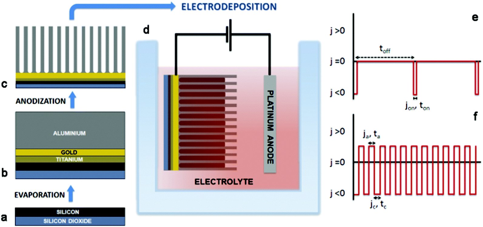 | ||
| Fig. 1 Schematic pictures of the synthesis procedure used to prepare the CoNi(Re)P nanowires: (a) evaporation of an insulating SiO2 layer at the backside of the Si substrate by plasma-enhanced chemical vapour deposition, (b) deposition of the Ti (adhesion), Au (seed) and Al layers onto the SiO2/Si substrate by means of e-beam evaporation, (c) anodization of the as-grown Al layer, and (d) electrodeposition of the nanowires inside the pores of the AAO templates. Also shown are the applied current density (j) vs. time (t) cycles corresponding to (e) the pulse plating conditions used to grow the NWs and, for comparison, (f) the reverse pulse plating conditions used for the growth of the continuous layers. Note that jon and jc denote the peak pulse current density and cathodic current density used for the growth of the NWs and the films, respectively. | ||
Fig. 2 depicts the mechanical characterization procedure used to measure the NWs. First, individual NWs were carefully adhered to a marked TEM grid using a special gluing procedure (Fig. 2a). Then, the NWs were nanoindented (Fig. 2b). Subsequently, the indented NWs were imaged by atomic force microscopy (AFM) (Fig. 2c and d). Contrary to other studies, the AFM tip was not directly used for nanoindentation since this poses problems in assuring that the AFM tip remains perpendicular to the surface during the entire test. Hence, slip friction artifacts, which would have made the study less reliable, were avoided.
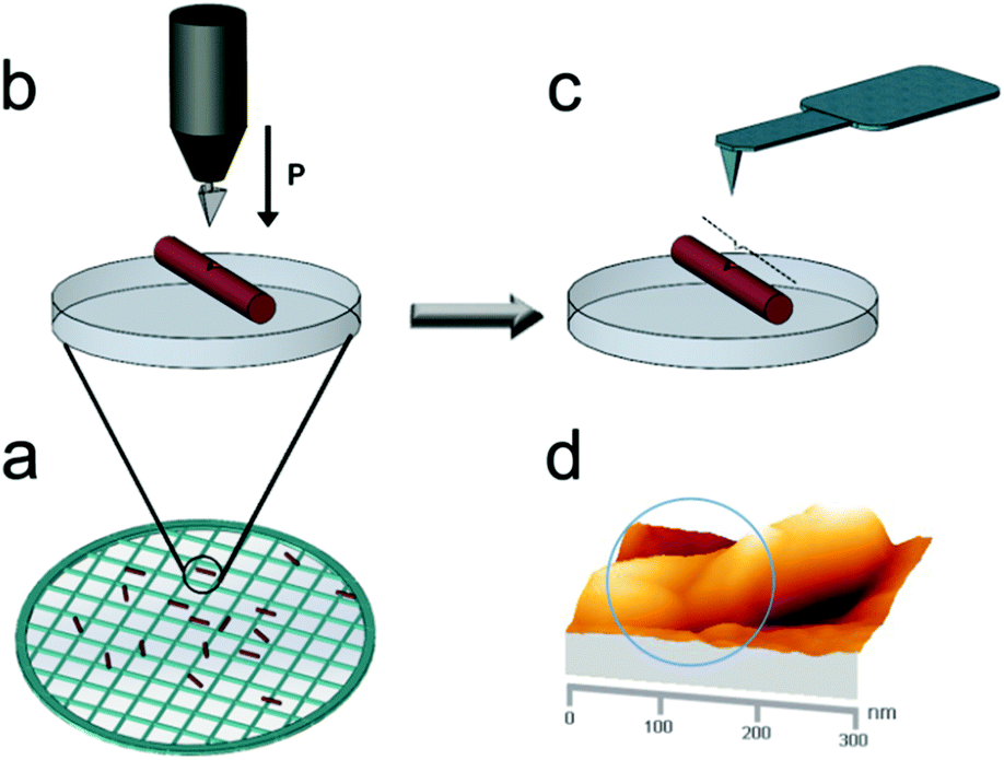 | ||
| Fig. 2 Schematic pictures of the indentation procedure, showing (a) an ensemble of NWs deposited dropwise onto the surface of an adherent coating previously deposited onto a TEM grid (which contained reference marks, not drawn), (b) the nanoindentation of a single NW using a conventional indenter tip, (c) subsequent imaging using an atomic force microscope (AFM) and (d) a real 3D AFM image corresponding to an indent performed onto a Co44Ni30Re12P14 amorphous NW. | ||
Fig. 3a shows a representative FIB cross-section of CoNi(Re)P NWs embedded in the AAO template. As can be observed, the length of the NWs is approximately 1 μm. Fig. 3b shows a TEM image of a bundle of Co75Ni11Re8P6 NWs (jc = −210 mA cm−2) obtained after removing the AAO matrix. Fig. 3c shows a detailed zoomed image of the morphology at the center of one of these NWs. The corresponding HRTEM image is presented in Fig. 3d. Lattice fringes can be clearly distinguished, thus showing the high crystallinity of the sample. The selected area electron diffraction (SAED) pattern in the inset displays spotty rings. Fig. 3e shows the HRTEM image and the SAED pattern of a ternary Co79Ni11P10 NW. In this case the crystallites are smaller compared to the previous sample. Accordingly, its SAED pattern features diffuse rings, indicating an ultra-nanocrystalline structure. Fig. 3f shows the TEM image and SAED pattern of an amorphous Co44Ni30Re12P14 NW.
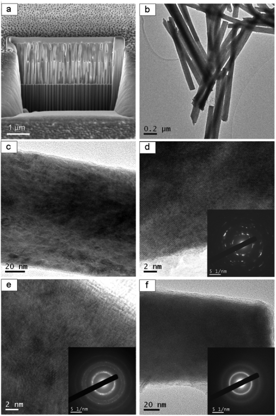 | ||
| Fig. 3 (a) Representative FESEM image of a FIB cross-section of the AAO template filled with CoNi(Re)P NWs, (b) TEM image of a bundle of Co75Ni11Re8P6 NWs, (c) and (d) TEM and HRTEM images of a crystalline Co75Ni11Re8P6 NW, (e) HRTEM image of an ultrananocrystalline Co79Ni11P10 NW, and (f) HRTEM image of an amorphous Co44Ni30Re12P14 NW. The insets in panels (d)–(f) show the corresponding SAED patterns. | ||
Further structural analysis of the NWs was performed using X-ray diffraction (XRD). The XRD pattern for the Co75Ni11Re8P6 NWs corresponds to an hcp solid solution (ESI Fig. S2†). These NWs are clearly textured in the (002) plane. In addition, the hcp reflections are shifted toward lower 2θ angles as compared to the tabulated positions for pure hcp-Co, due to the incorporation of Re (with a large atomic radius) in the hcp structure. The XRD pattern for the Co79Ni11P10 NWs shows broad reflections corresponding to the hcp phase, but the (100) preferred orientation clearly increases at the expense of the (002) texture. Finally, the Co44Ni30Re12P14 NWs show an amorphous structure, as evidenced by the broad halo centered at 2θ ≈ 44°. The formation of amorphous CoNiReP NWs is mainly attributed to the increase in both the Re and P content, which is in agreement with previous work on electrodeposition of CoNiReP continuous films.23,26 The XRD patterns of the CoNi(Re)P continuous films with analogous compositions are also shown in ESI Fig. S2.† The Co74Ni11Re10P5 film is crystalline (hcp structure) and is textured in the (002) plane. The ternary Co80Ni11P9 also shows an hcp structure. Finally, the Co42Ni34Re11P13 film is entirely amorphous.
3.2. Mechanical properties and finite element modelling
Representative nanoindentation curves of the samples listed in Table 1 are plotted in Fig. 4. Interestingly, while for nanocrystalline alloys the maximum penetration depth is larger for films than for homologous NWs (Fig. 4b and c), the opposite is observed for glassy samples (Fig. 4a). In general, caution must be taken when comparing the nanomechanical properties of small samples with those tabulated for bulk samples. Hardness depends on the applied load during nanoindentation. This “indentation size effect (ISE)” is due to the need to create geometrically-necessary dislocations in small indentations in crystalline materials and to deformation-induced creation of free volume in amorphous alloys.5,27 Hence, the properties of nanoscale objects and those of the corresponding bulk materials should ideally be measured under the same experimental conditions (applied load, strain rate, etc.) in order to be comparable. This is why the same low value of maximum applied load is used here for both the NWs and the films.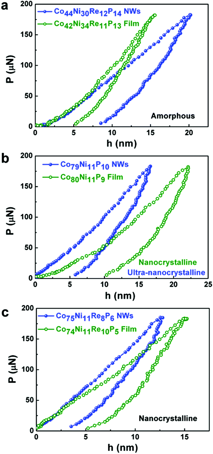 | ||
| Fig. 4 Representative nanoindentation curves obtained from the films and individual nanowires, corresponding to: (a) the amorphous quaternary alloy, (b) the ternary nanocrystalline alloy and (c) the quaternary nanocrystalline alloy. | ||
The values of H and reduced Young's modulus (Er) calculated using the conventional method of Oliver and Pharr are listed in Table 1 and, as expected from the load-displacement curves, the amorphous NWs are apparently softer than the glassy films. However, this model does not take into account the curvature of the NWs. By geometrically considering the actual tip radius (approximately 250 nm) and the diameter of the NWs (100 nm), an estimate of how the contact area (and therefore H and Er) becomes modified compared to indentation on a flat surface can be made. Taking this into account, H in the NWs (both crystalline and amorphous) is dramatically enhanced with respect to the films (for example, from 7.6 GPa to the unrealistic value of 36 GPa for the Co44Ni30Re12P14 NWs, see the ESI†).
A more accurate approach is to perform three-dimensional (3D) FEM taking the following issues into account: (i) the radius of curvature of the tip, (ii) the effect of curvature of the NWs on the resulting contact area, (iii) the lack of lateral confinement in the NWs (i.e., constraint factor), (iv) the possible influence of the substrate, (v) eventual pile-up/sink-in effects and (vi) the actual yielding criterion operative in the glassy and crystalline alloys.
Remarkably, yielding in metallic glasses cannot be simply described by the usual von Mises or Tresca criteria, as for crystalline metals, since normal stress components acting on the shear plane play a key role at the onset of plasticity.5,28–30 This effect, which needs to be taken into account in the simulations, is captured by the Mohr–Coulomb yield criterion, which is expressed as τy = c − βM–C × σn, where τy is the shear stress on the slip plane at yielding, c is the shear strength in pure shear (also termed cohesive stress), σn is the normal stress acting on the shear plane and βM–C denotes the internal friction coefficient. The simulations on the amorphous continuous film reveal that this alloy exhibits E = 151 GPa, a friction angle of 11° (βM–C = 0.194) and a cohesive stress of 2 GPa (Fig. 5a). From the contact area, as determined by the 3D model, a hardness of 12.0 GPa is obtained for the amorphous film, which is slightly larger than the value directly determined using the method of Oliver and Pharr (HO–P = 8.9 GPa, see Table 1). This difference is ascribed to the presence of the sink-in, as evidenced in Fig. 5c. If the same parameters (c = 2 GPa, βM–C = 0.194, E = 151 GPa) are used to model the nanoindentation behavior of the amorphous NWs (curves in blue in Fig. 5b), the penetration depth is largely overestimated for any given value of the applied load, both considering elastic or rigid substrates. An agreement between the calculated and the experimental load-displacement indentation curves necessarily required lowering E and βM–C while significantly enhancing the cohesive stress (i.e., E = 140 GPa, βM–C = 0.123 and c = 9 GPa) and using a rigid substrate (see Fig. 5b). Similar to the case of the amorphous film, H in the glassy nanowire was directly determined from the contact area assessed from the FEM, leading to HSim = 23 GPa. Hence, the amorphous NWs clearly exhibit a lower friction coefficient and Young's modulus but a higher hardness than the glassy films, once the nanoindentation results are properly interpreted with the use of the 3D FEM. The evolution of the stress contour mappings as a function of the applied load, both for the amorphous films and NWs, is shown in Movies V1 and V2 of the ESI.† The slight curvature of the loading part of the simulated nanoindentation curve is related to barreling of the nanowire (Fig. 5e). Due to this barreling, the cross section of the nanowire becomes flattened, as evidenced in Fig. 5d and f. The 3D FEM provides significant insight, because it reveals that the amorphous NWs are in fact not mechanically softer (as predicted by the method of Oliver and Pharr), but mechanically harder (see Table 1). The 3D FEM was also used to estimate H of the crystalline films and NWs (using the Tresca yield criteria). Although the agreement between the experimental and simulated curves was not as good in this case (see the ESI†), it is clear that the relative increase of H between the nanocrystalline films and NWs is much larger than that observed between the amorphous films and NWs (Table 1).
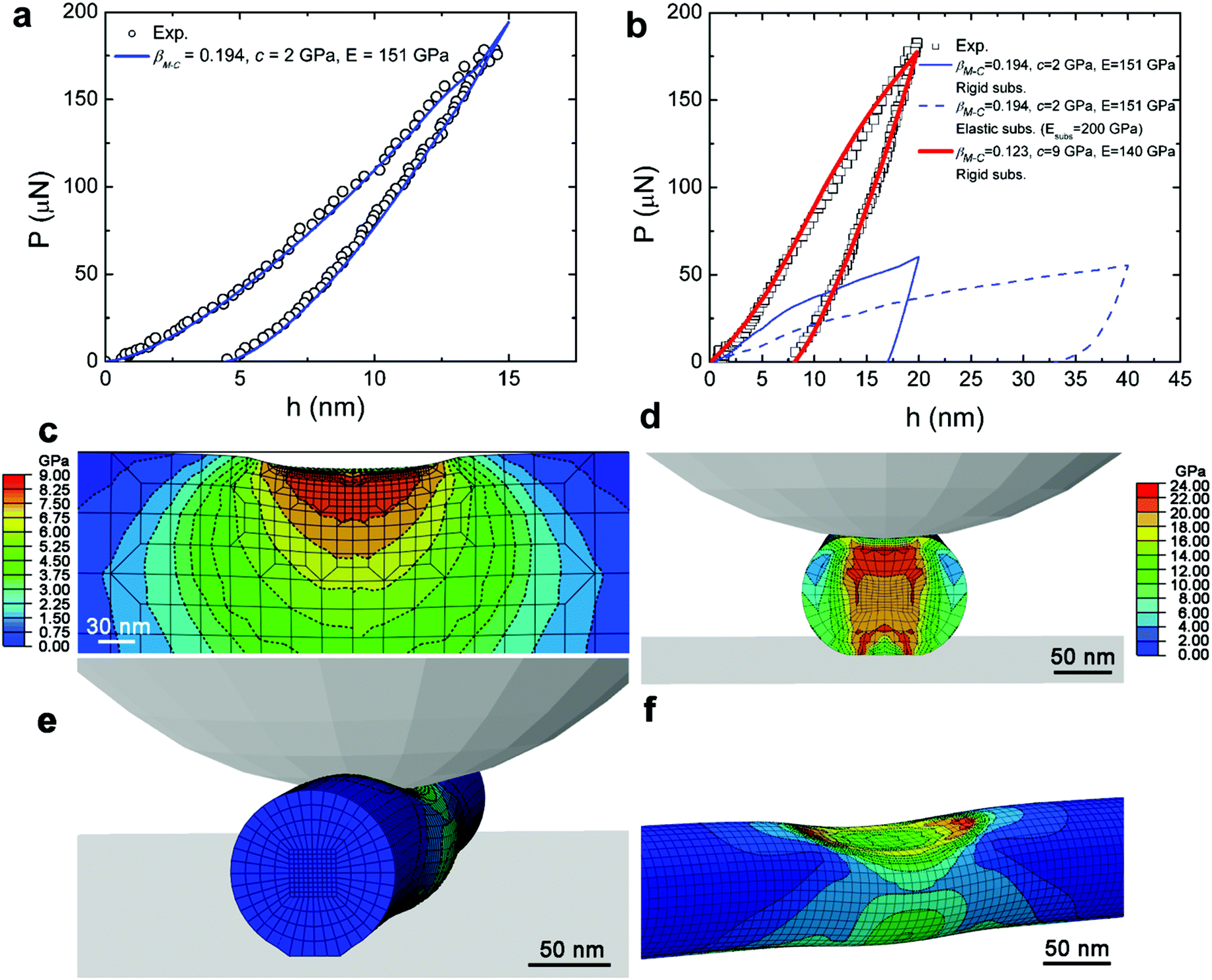 | ||
| Fig. 5 Computed load–unload nanoindentation curves of (a) the amorphous continuous film and (b) the glassy nanowires using the Mohr–Coulomb yield criterion with values of the friction coefficient, βM–C, and cohesive strength, c, that provide good agreement with the experimental curves. Shown in blue in panel (b) are two additional computed curves (one considering a rigid substrate and the other a fully elastic substrate), where the same values of c, βM–C and Young's modulus as for the continuous films have been utilized (without giving a good adjustment to the experimental curve). Panel (c) shows the Tresca stress contour mapping at the maximum load corresponding to the simulated amorphous film (note the sink-in effect at the edges of the indentation impression). Panels (d)–(f) show the Tresca stress contour mappings at the maximum load of the indented nanowire in different perspectives (panel (d) shows the cross section just underneath the indenter tip). Note that the overall mesh distribution (nodes and plates) is displayed in the images. | ||
Table 1 also lists the values of the plasticity index (Upl/Utot, where Upl and Utot are the plastic and total indentation energies). Remarkably, the area encompassed between the loading and unloading segments (the plasticity index) is reduced in the amorphous film compared to the NWs (and vice versa for the crystalline alloys). The reduced sample size of the amorphous NWs also appears to cause deviations from the deformation map proposed by Schuh et al.,31 since plastic flow was found to be homogeneous in spite of the relatively slow indentation strain rates (see the ESI†).
The difference in H and Er between the crystalline NWs and films could be ascribed to the existing crystallographic texture, differences in the mean crystallite size and sample size effects (see the ESI† for a detailed description of these effects).32–36 Unlike crystalline alloys, metallic glasses do not deform by the propagation of dislocations but via activation of “shear transformation zones (STZ)”, which are clusters of atoms that move together under the action of a shear stress.6 The configuration rearrangements of STZ are accompanied by the creation of free volume, which locally coalesces to form embryonic shear bands. The rapid propagation of fully-developed shear bands leads to mechanical softening and catastrophic failure. In brittle materials (such as metallic glasses), an increase of yield stress (and H) with the decrease of sample size is expected since the probability of finding the pre-existing mechanically-weak flaws (which are nucleation sites for shear bands) is lower for smaller samples. Following this reasoning, an increase of yield stress with the reduction of sample size can be anticipated for micrometer-sized amorphous samples where deformation is still heterogeneous.7 However, shear band activity is totally inhibited in samples of reduced dimensions (of the order of 100 nm) or if the applied load is sufficiently low.7,37–39 In the homogeneous deformation regime (as in the NWs herein investigated), the dependence of the yield stress on the sample size remains less explored and poorly understood. As the sample size becomes comparable to the shear band thickness (ca. 20–30 nm), the number of flaw sites for favorable shear band initiation becomes highly reduced. In the limiting case of a flawless metallic glass, the stress for homogeneous deformation would become much higher than the stress required for the onset of heterogeneous plastic flow, as the main plastic deformation mechanism of metallic glasses (i.e., the propagation and branching of shear bands) would be precluded. On the other hand, in nanoscale samples (both crystalline and amorphous), the high surface area-to-volume ratio promotes surface diffusion effects that can a priori lead to elastic softening. Surface atoms are less constrained than the inner ones, thereby making the NW easier to deform in the elastic regime. This reasoning can explain the decrease of Er in the glassy NWs compared to the corresponding films. The increase of the plasticity index observed in the amorphous Co44Ni30Re12P14 NWs with respect to the homologous glassy films is also probably due to the enhanced surface diffusion paths that promote a larger plastic flow compared to the glassy films that also deform in the homogeneous regime. Such effects are less clear for the crystalline NWs probably because the long-range crystallographic order makes all atoms (irrespective of their location in the NW) more stiffly bonded. Our results indicate that the relative changes in the hardness in the crystalline NWs are larger than that in the amorphous NWs. This observation is probably related to the profound effects of lateral confinement on the nucleation and propagation of dislocations inside the NWs, which causes stress concentrations similar to the Hall–Petch effect. The moderate increase of H in the glassy NWs is probably linked to the lower probability of finding flaw defects for free volume creation as compared to the glassy films. The lack of shear bands in the NWs (due to their small size) also avoids strain softening which usually occurs in bulk metallic glasses. Furthermore, a high plasticity index in the amorphous NWs means that even if the sample starts to plastically deform, the specimen will not suddenly fail, as usually happens in bulk metallic glasses. Therefore, amorphous NWs overcome, at least to some extent, one of the main drawbacks of the mechanical performance of bulk metallic glasses, i.e., their limited plasticity and high brittleness. The results suggest that the mechanical endurance (i.e., life-time) of patterned metallic glasses is possibly significantly higher than that of patterned crystalline alloys, where the plasticity index is lower. This effect is important for the use of these materials in any kind of micro-/nano-electromechanical system, such as in small sensors, actuators, micro-/nano-robots, micro-gears, ultra-sharp micro-blades, surgical micro-scissors, etc.9,40,41
Finally, since no pop-in events are observed in the loading curves of the amorphous films and nanowires, any difference in H or Er between both types of samples can be linked to the changes in the cohesive stress or internal friction coefficient. As indicated in Fig. 5, the cohesive stress increases from 2 GPa (in the films) to 9 GPa (in the nanowires), whereas βM–C decreases from 0.194 in the films to 0.123 in the NWs. The smaller βM–C obtained in the NWs suggests that glassy nanowires deviate less significantly from the yielding criterion of crystalline materials (i.e., Tresca) as compared to the amorphous films. This is opposite to what is encountered in thermally-annealed metallic glasses, where the annihilation of free volume increases the pressure-sensitivity index (i.e., the value of βM–C).42
4. Conclusions
In summary, comparative nanoindentation studies of electrodeposited metallic NWs and μm thick films reveal dissimilar nanomechanical behavior at the nanoscale depending on whether the investigated alloys are amorphous or crystalline. While the lateral physical constraints imposed by the reduced sample dimensions of the NWs induce an increase of H and E (and a decrease of the plasticity index) in the crystalline compositions, opposite trends in E and plasticity are observed in the case of nanoscale glassy specimens. The different deformation mechanisms in both types of materials are discussed in detail. This work also provides clear protocols on how to investigate the nanomechanical properties of cylindrical NWs deposited onto rigid substrates using nanoindentation. In particular, we show the importance of taking the curved geometry of the specimens into account. The results reveal that the conventional method of Oliver and Pharr is not applicable to the case of indented nanowires. From a fundamental point of view, our results shed light on the intricate deformation behavior of ultra-small glassy samples whose plastic flow occurs without shear band activity. The high intrinsic plasticity of the amorphous NWs is of technological relevance since this parameter contributes to enhance the endurance of any structural component used in micro-/nano-devices.Acknowledgements
The authors acknowledge Prof. A. L. Greer for the critical reading of the manuscript and his insightful comments. We also acknowledge Dr Emma Rossinyol and Jin Zhang for their assistance in TEM sample preparation and graphical designs, respectively. We are also thankful to Dr A.C. Fischer-Cripps for his useful comments on the interpretation of the nanoindentation data acquired on the curved surface of the nanowires. Partial financial support from the MAT2011-27380-C02-02 and the 2014 SGR-1015 research projects from the Spanish MINECO and the Generalitat de Catalunya is acknowledged. The authors also acknowledge funding support from the European Community's Seventh Framework Programme (FP7/2007-2013) under grant agreement 296679 (MANAQA). E.P. acknowledges the Spanish Ministerio de Economía y Competitividad (MINECO) for the ‘Ramon y Cajal’ contract (RYC-2012-10839). ICN2 acknowledges support from the Severo Ochoa Program (MINECO, Grant No. SEV-2013-0295).References
- J. R. Greer, D. Jang, J.-Y. Kim and M. J. Burek, Adv. Funct. Mater., 2009, 19, 1–7 CrossRef.
- B. Wu, A. Heidelberg and J. J. Boland, Nat. Mater., 2005, 4, 525–529 CrossRef CAS PubMed.
- Y. Lu, J. Y. Huang, C. Wang, S. Sun and J. Lou, Nat. Nanotechnol., 2010, 5, 218–224 CrossRef CAS PubMed.
- X. Li, X. Wang, Q. Xiong and P. C. Eklund, Nano Lett., 2005, 5, 1982–1986 CrossRef CAS PubMed.
- J. Fornell, A. Concustell, S. Suriñach, W. H. Li, N. Cuadrado, A. Gebert, M. D. Baró and J. Sort, Int. J. Plast., 2009, 25, 1540–1559 CrossRef CAS.
- C. A. Schuh, T. C. Hufnagel and U. Ramamurty, Acta Mater., 2007, 55, 4067–4109 CrossRef CAS.
- A. L. Greer, Y. Q. Cheng and E. Ma, Mater. Sci. Eng., R, 2013, 74, 71–132 CrossRef.
- J. H. Luo, F. F. Wu, J. Y. Huang, J. Q. Wang and S. X. Mao, Phys. Rev. Lett., 2010, 104, 215503 CrossRef CAS PubMed.
- K. S. Nakayama, Y. Yokoyama, T. Ono, M. W. Chen, K. Akiyama, T. Sakurai and A. Inoue, Adv. Mater., 2010, 22, 872–875 CrossRef CAS PubMed.
- D. Jang and J. R. Greer, Nat. Mater., 2010, 9, 215–219 CAS.
- S. Cheng, X.-L. Wang, H. Choo and P. K. Liaw, Appl. Phys. Lett., 2007, 91, 201917 CrossRef.
- C. C. Wang, J. Ding, Y.-Q. Cheng, J.-C. Wan, L. Tian, J. Sun, Z.-W. Shan, J. Li and E. Ma, Acta Mater., 2012, 60, 5370–5379 CrossRef CAS.
- C. A. Volkert, A. Donohue and F. Spaepen, J. Appl. Phys., 2008, 103, 083539 CrossRef.
- Y. J. Huang, J. Shen and J. F. Sun, Appl. Phys. Lett., 2007, 90, 081919 CrossRef.
- B. E. Schuster, Q. Wei, T. C. Hufnagel and K. T. Ramesh, Acta Mater., 2008, 56, 5091–5100 CrossRef CAS.
- O. V. Kuzmin, Y. T. Pei, C. Q. Chen and J. Th. de Hosson, Acta Mater., 2012, 60, 889–898 CrossRef CAS.
- H. Bei, Z. P. Lu, S. Shim, G. Chen and E. P. George, Metall. Mater. Trans. A, 2010, 41, 1735–1742 CrossRef.
- Q. Guo, P. Landau, P. Hosemann, Y. Wang and J. R. Greer, Small, 2013, 9, 691–696 CrossRef CAS PubMed.
- D. J. Magagnosc, R. Ehrbar, G. Kumar, M. R. He, J. Schroers and D. S. Gianola, Sci. Rep., 2013, 3, 1096 Search PubMed.
- J. R. Greer and J. Th. de Hosson, Prog. Mater. Sci., 2011, 56, 654–724 CrossRef CAS.
- X. Li, H. Gao, C. J. Murphy and K. K. Caswell, Nano Lett., 2003, 3, 1495–1498 CrossRef CAS.
- X. Tao, X. Wang and X. Li, Nano Lett., 2007, 7, 3172–3176 CrossRef CAS PubMed.
- S. Pané, E. Pellicer, K. M. Sivaraman, S. Suriñach, M. D. Baró, B. J. Nelson and J. Sort, Electrochim. Acta, 2011, 56, 8979–8988 CrossRef.
- W. C. Oliver and G. M. Pharr, J. Mater. Res., 1992, 7, 1564–1583 CrossRef CAS.
- Y.-J. Kim, K. Son, I.-C. Choi, I.-S. Choi, W. Park and J. Jang, Adv. Funct. Mater., 2011, 21, 279–286 CrossRef CAS.
- D. P. Daly and F. J. Barry, Int. Mater. Rev., 2003, 48, 326–338 CrossRef.
- N. Van Steenberge, J. Sort, A. Concustell, J. Das, S. Scudino, S. Suriñach, J. Eckert and M. D. Baró, Scr. Mater., 2007, 56, 605–608 CrossRef CAS.
- F. S. Santos, J. Sort, J. Fornell, M. D. Baró, S. Suriñach, C. Bolfarini, W. J. Botta and C. S. Kiminami, J. Non-Cryst. Solids, 2010, 356, 2251–2257 CrossRef CAS.
- C. A. Schuh and A. C. Lund, Nat. Mater., 2003, 2, 449–452 CrossRef CAS PubMed.
- R. Vaidyanathan, M. Dao, G. Ravichandran and S. Suresh, Acta Mater., 2001, 49, 3781–3789 CrossRef CAS.
- C. A. Schuh, A. C. Lund and T. H. Nieh, Acta Mater., 2004, 52, 5879–5891 CrossRef CAS.
- R. D. Arnell, J. Phys. D: Appl. Phys., 1974, 7, 1225–1232 CAS.
- D. Tromans, Int. J. Res. Rev. Appl. Sci., 2011, 6, 462–483 Search PubMed.
- E. W. Wong, P. E. Sheehan and C. M. Lieber, Science, 1997, 277, 1971–1975 CrossRef CAS.
- Q. Xiong, N. Duarte, S. Tadigadapa and P. C. Eklund, Nano Lett., 2006, 6, 1904–1909 CrossRef CAS PubMed.
- H. Zheng, A. Cao, C. R. Weinberger, J. Y. Huang, K. Du, J. Wang, Y. Ma, Y. Xia and S. X. Mao, Nat. Commun., 2010, 1, 144 CrossRef PubMed.
- B.-G. Yoo, J.-Y. Kim, Y.-J. Kim, I.-C. Choi, S. Shim, T. Y. Tsui, H. Bei, U. Ramamurty and J.-I. Jang, Int. J. Plast., 2012, 37, 108–118 CrossRef CAS.
- C. Q. Chen, Y. T. Pei and J. T. M. De Hosson, Acta Mater., 2010, 58, 189–200 CrossRef CAS.
- C. Q. Chen, Y. T. Pei, O. Kuzmin, Z. F. Zhang, E. Ma and J. T. M. De Hosson, Phys. Rev. B: Condens. Matter, 2011, 83, 180201(R) CrossRef.
- J. P. Chu, J. S. C. Jang, J. C. Huang, H. S. Chou, Y. Yang, J. C. Ye, Y. C. Wang, J. W. Lee, F. X. Liu and P. K. Liaw, Thin Solid Films, 2012, 520, 5097–5122 CrossRef CAS.
- P. Sharma, N. Kaushik, H. Kimura, Y. Saotome and A. Inoue, Nanotechnology, 2007, 18, 035302 CrossRef PubMed.
- A. Dubach, K. E. Prasad, R. Raghavan, J. F. Löffler, J. Michler and U. Ramamurty, J. Mater. Res., 2009, 24, 2697–2704 CrossRef CAS.
Footnotes |
| † Electronic supplementary information (ESI) available: Additional details on experimental and analysis methods, additional results on crystalline CoNi(Re)P alloys and two movies to illustrate the stress distribution during deformation of the amorphous and crystalline nanowires. See DOI: 10.1039/c5nr04398k |
| ‡ Both authors contributed equally to the present work. |
| This journal is © The Royal Society of Chemistry 2016 |