
 Open Access Article
 This Open Access Article is licensed under a Creative Commons Attribution-Non Commercial 3.0 Unported Licence
Effect of relative humidity on crystal growth, device performance and hysteresis in planar heterojunction perovskite solar cells†
Mahesh K.
Gangishetty
,
Robert W. J.
Scott
and
Timothy L.
Kelly
*
Department of Chemistry, University of Saskatchewan, 110 Science Place, Saskatoon, SK, Canada. E-mail: tim.kelly@usask.ca; Fax: +1 306 966-4730; Tel: +1 306 966-4666
First published on 21st September 2015
Abstract
Due to the hygroscopic nature of organolead halide perovskites, humidity is one of the most important factors affecting the efficiency and longevity of perovskite solar cells. Although humidity has a long term detrimental effect on device performance, it also plays a key role during the initial growth of perovskite crystals. Here we demonstrate that atmospheric relative humidity (RH) plays a key role during the formation of perovskite thin films via the sequential deposition technique. Our results indicate that the RH has a substantial impact on the crystallization process, and hence on device performance. SEM and pXRD analysis show an increase in crystallite size with increasing humidity. At low RH, the formation of small cubic crystallites with large gaps between them is observed. The presence of these voids adversely affects device performance and leads to substantial hysteresis in the device. At higher RH, the perovskite crystals are larger in size, with better connectivity between the crystallites. This produced efficient planar heterojunction solar cells with low hysteresis. By careful control of the RH during the cell fabrication process, efficiencies of up to 12.2% are reached using P3HT as the hole-transport material.
Introduction
Perovskite solar cells have attracted a great deal of interest in the field of solid state photovoltaics due to their large extinction coefficients and long charge carrier diffusion lengths.1–4 Within a period of 5 years the efficiency of these devices has dramatically increased from 3.8% to 20.1%, making them one of the most promising alternatives to conventional silicon and CdTe technology.5–14In the fabrication of high performance perovskite solar cells, the quality of the perovskite film plays a critical role.15 Recently, it was found that the presence of grain boundaries in the perovskite film can affect not only the performance of the device, but also the amount of hysteresis observed in the J–V curves.16,17 As a result, a number of strategies for the production of high quality perovskite films have been reported, including the addition of chloride additives,17–20 solvent engineering,13 and moisture6,21 and solvent annealing.22 By using the interdiffusion method, Im et al. produced large perovskite crystallites, which led to state-of-the-art mesoscopic solar cells.12 Nie et al., by keeping the substrate above room temperature during the deposition process, were able to prepare high quality films containing millimeter scale perovskite crystallites with few grain boundaries.11 This resulted in high performance, hysteresis-free devices with efficiencies of up to 18%. The importance of grain boundaries on the electronic properties of perovskite thin films was recently highlighted by recent work on perovskite single crystals; these studies suggest that the carrier diffusion lengths of CH3NH3PbI3 single crystals are at least 2 μm,4 and may exceed 175 μm.1
The formation of high quality perovskite films depends not only on the deposition process, but also on the atmospheric conditions present during crystal growth. Due to the highly hygroscopic nature of CH3NH3PbI3, the relative humidity (RH) is a key factor in both the growth and the degradation of perovskite crystals. Several research groups have observed that exposing perovskite films to high levels of moisture leads to degradation of the perovskite and the formation of hydrate phases;23–27 this in turn rapidly leads to device failure. Despite this problem, humidity has also been shown to have beneficial effects on the initial growth of perovskite films. Bass et al. observed that when CH3NH3PbX3 (X = I, Br) powders were prepared under rigorously anhydrous conditions, the resulting powders showed very little long-range order; however, upon exposure to moisture, they immediately crystallized.28 Similarly, by post-annealing perovskite films under a relative humidity of 30 ± 5%, Zhou et al. were able to achieve uniform, crystalline, and pinhole-free perovskite films.6 By increasing the relative humidity from 20% to 80% during the post-annealing step, further increases in the crystallinity of the perovskite films were observed.21 Spin coating the PbCl2 and CH3NH3I precursors under low RH conditions and subsequently annealing them under higher RH has also been shown to lead to improvements in long-range order and device performance.29 However, all of these reports employed the single-step deposition method, where the effect of relative humidity was investigated during the post-annealing step. Analogous studies on the effect of humidity on films deposited via the two-step (sequential) deposition method30,31 are lacking. Since the mechanism of crystal growth and subsequent film morphology are strongly dependent on the deposition method, the role of the RH during the sequential deposition of perovskite thin films needs to be addressed.
Here we demonstrate the effect of relative humidity on the growth of perovskite thin films deposited by the sequential deposition method. PbI2 films were converted into CH3NH3PbI3 inside a chamber of controlled RH, and larger perovskite crystallites were observed at higher RHs. This resulted in the formation of densely packed films with fewer grain boundaries, leading to an increase in device performance and a reduction in J–V curve hysteresis. By careful control of the RH, devices with power conversion efficiencies of 12.2% were prepared using poly(3-hexylthiophene) (P3HT) as the hole transport material (HTM).
Experimental section
Materials
Lead(II) iodide (99%), methylamine (37% in absolute ethanol), hydriodic acid (57% in H2O), 4-tert-butylpyridine (96%) and lithium-bis(trifluoromethanesulfonyl)imide (99%) were purchased from Sigma-Aldrich. Poly(3-hexylthiophene) (electronic grade) and Ag pellets (99.99%) were purchased from Rieke Metals and Kurt J. Lesker, respectively. All commercial reagents were used as received. Zinc oxide nanoparticles7 and methylammonium iodide32 were synthesized according to established procedures.Device fabrication
Fabrication procedures for perovskite solar cells were similar to those outlined in our previous report.33 ITO-coated glass substrates (Delta Technologies, Rs = 15–25 Ω sq−1) were cleaned by sequentially sonicating them for 30 min in 2% Extran 300 detergent and isopropanol, followed by drying under a stream of air. A thin layer of ZnO nanoparticles (NPs) was spin coated at 3000 rpm for 30 s using a 6 mg mL−1 colloidal ZnO NP solution in n-butanol. This procedure was repeated three times to produce a uniform 20 nm ZnO NP layer. A layer of PbI2 (150 nm) was then deposited by thermal evaporation at a base pressure of 2 × 10⁻⁶ mbar. The PbI2 films were then brought into a sealed atmospheric bag that was maintained at a constant RH (1–60%, Fig. 1) and dipped in a solution of 10 mg mL−1 CH3NH3I in isopropanol for 3 min. After dipping, the substrates were dried by spinning at 3000 rpm for 30 s, and then allowed to dry further inside the atmospheric bag for 10 minutes. A thin layer of P3HT-based hole transport material (20 mg of P3HT, 3.4 μL of 4-tert-butylpyridine, and 6.8 μL of a lithium-bis(trifluoromethanesulfonyl)imide (Li TFSI) solution (28 mg Li-TFSI/1 mL acetonitrile) all dissolved in 1 mL chlorobenzene) was spin coated at 1000 rpm for 30 s under ambient conditions. Finally, a 50 nm thick Ag layer was deposited by thermal evaporation at a base pressure of 2 × 10⁻⁶ mbar.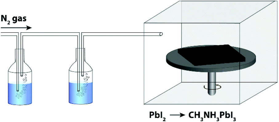 | ||
| Fig. 1 Schematic of the apparatus used to control the RH inside an atmospheric bag containing a spin coater. PbI2 films are converted into CH3NH3PbI3 by immersion in a solution of CH3NH3I, spin dried at 3000 rpm for 30 s, and allowed to dry for a further 10 min. | ||
Characterization
UV-Vis spectra were recorded on a Cary 6000 spectrophotometer. Scanning electron microscopy was carried out on a Hitachi SU8010 SEM operating at a 1.0–5.0 kV landing voltage. Powder X-ray diffraction (pXRD) was performed on a PANalytical Empyrean diffractometer configured with a copper (λ = 1.54 Å) X-ray source. J–V curves were recorded in a N2-filled glovebox using a Keithley 2400 source-measure unit and a 450 W Class AAA solar simulator equipped with an AM1.5G filter (Sol3A, Oriel Instruments), at a calibrated intensity of 100 mW cm−2, as determined by a standard silicon reference cell (91![[thin space (1/6-em)]](https://www.rsc.org/images/entities/char_2009.gif) 150 V, Oriel Instruments). The effective area of the device was defined as 0.0708 cm2 using a non-reflective metal mask. Incident photon-to-current (IPCE) spectra were measured in a N2-filled glovebox using a commercial IPCE setup (QE-PV-Si, Oriel Instruments). Monochromatic light was chopped at a frequency of 8 Hz and photocurrents measured using a lock-in amplifier.
150 V, Oriel Instruments). The effective area of the device was defined as 0.0708 cm2 using a non-reflective metal mask. Incident photon-to-current (IPCE) spectra were measured in a N2-filled glovebox using a commercial IPCE setup (QE-PV-Si, Oriel Instruments). Monochromatic light was chopped at a frequency of 8 Hz and photocurrents measured using a lock-in amplifier.
Results and discussion
Effect of humidity on perovskite crystal growth
In order to investigate the role of relative humidity in the growth of perovskite crystals during the sequential deposition process, an atmospheric bag of controllable RH was used (Fig. 1). In this setup, dry N2 was used as the carrier gas, and was flowed through a set of water bubblers into the atmospheric bag. A portable RH sensor was used to measure the humidity inside the bag, and the RH was controlled by adjusting the flow rate of the carrier gas. After achieving the desired humidity, the perovskite layer was deposited by the sequential deposition method. The device architecture used here is very similar to that described in our previous reports.7,33 A thin layer of ZnO was first deposited on ITO-coated glass, followed by a layer of PbI2. In order to ensure the formation of reproducible PbI2 films (and to eliminate any effect of varying humidity on the PbI2 deposition step), the PbI2 films were deposited by thermal evaporation. After deposition, the ITO/ZnO/PbI2 films were brought into the atmospheric bag (which was maintained at the desired RH), and then immediately dipped into a solution of CH3NH3I. After 3 minutes of immersion, excess CH3NH3I solution was removed by spinning at 3000 rpm for 30 s. The perovskite films were then allowed dry for a further 10 min inside the controlled RH environment.Perovskite films were prepared with RH ranging from 1% to 60%, and subsequently characterized by UV-Vis spectroscopy, pXRD and SEM. The absorption spectra of the films are shown in Fig. 2a. The spectra are all qualitatively similar, consisting of intense absorption bands below 500 nm and a sharp band edge feature at 760 nm. With increasing RH, a small but steady increase in the optical density of the films is observed. At low RH (1%), the films were transparent and light brown in color, and as the RH increased, the films became both darker and more opaque (Fig. 2b). Of all the samples studied, the perovskite films prepared at 60% RH showed the highest optical density across the entire visible spectrum. Further differences between the films become apparent at wavelengths close to the band edge (Fig. 2a inset). All of the films showed a sharp decrease in the optical density, except the one prepared at 1% RH. Instead, it displayed a more gradual decay in the optical absorption, known as an Urbach tail.34 This red tail in the optical absorption spectrum is attributed to electronic disorder within the film, and may be caused by the presence of trap states produced by incomplete formation of the perovskite.17,35
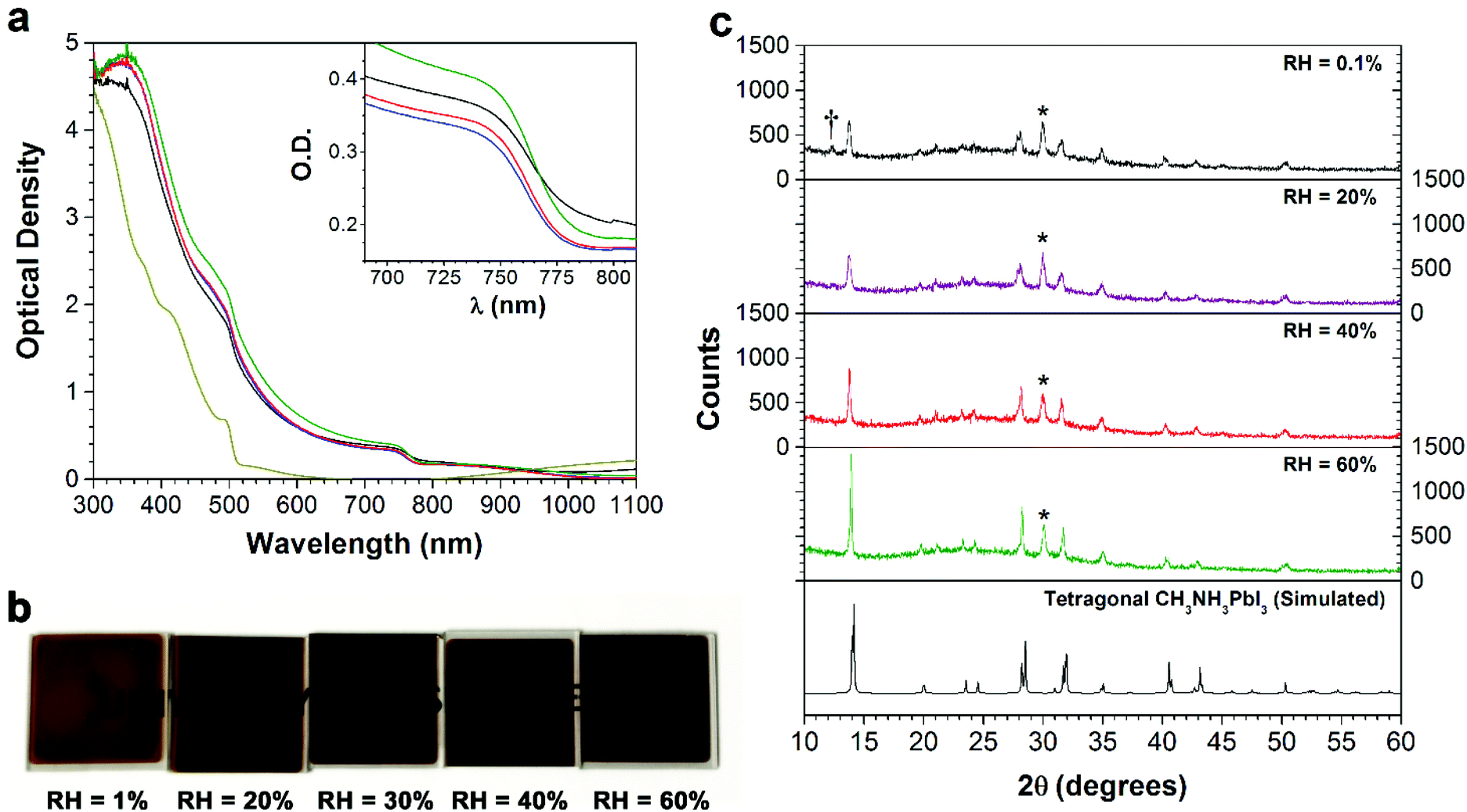 | ||
| Fig. 2 (a) UV-Vis absorption spectra for vapor deposited PbI2 thin films (yellow line), and CH3NH3PbI3 thin films prepared at 1% (black line), 33% (blue line), 40% (red line), and 60% (green line) RH. (b) Photographs of CH3NH3PbI3 thin films prepared at various RH values. (c) Powder X-ray diffraction patterns for ITO/PbI2/CH3NH3PbI3 thin films prepared at various RH values. Peaks due to ITO and PbI2 are marked with an asterisk (*) and dagger (†), respectively. | ||
In order to understand the effect of RH on the crystallinity of the perovskite films, each of the samples was characterized by pXRD (Fig. 2c). The diffraction pattern for all films agrees with the tetragonal structure of CH3NH3PbI3.36 The key differences observed between the samples are an increase in the intensity of the perovskite Bragg peaks (particularly the (110) and (220) reflections at ca. 14° and 28°), and a decrease in the peak width as the RH is increased. This indicates an increase in the size of the coherent scattering domains, suggesting the formation of larger crystallites at higher RH. Analysis of the (110) reflection by means of the Scherrer equation yielded minimum crystallite sizes of 25, 26, 40 and 61 nm for the films made at 0.1%, 20%, 40% and 60% RH, respectively. Additionally, at the lowest (0.1%) RH, there is a weak peak corresponding to PbI2, indicating incomplete formation of the perovskite under this low humidity condition. This is consistent with the presence of an Urbach tail in the absorption spectrum of this sample, and both the small crystallite size (with the associated increase in the number of surface states) and the residual PbI2 may contribute to the observed electronic disorder.
These changes in crystallite size and film morphology were imaged by SEM. Fig. 3 shows SEM images of both PbI2 (Fig. 3a) and perovskite films (Fig. 3b–f). The vapor deposited PbI2 film consisted of hexagonal flake-like structures (Fig. 3a), in agreement with previous reports of thermally evaporated films.33 Importantly, the SEM image of the perovskite film prepared at 1% RH showed small, cube-like crystallites with substantial empty space between them. As the RH increased to 20% RH, the film still appeared to consist of distinct cubic crystallites, but with improved connectivity between the grains. As the RH increased to 30% and above, the films became smoother and more planar, with fewer gaps between individual grains. As the RH increased further, there was a corresponding increase in the crystallite size, leading to more densely packed perovskite films. At the highest (60%) RH, the individual grains lost their distinctive cubic shape, and appeared more rounded; the edges of adjacent particles also appear to have fused together, providing much better connectivity within the film. These changes in crystallite size are consistent with the results of the Scherrer analysis of the pXRD data.
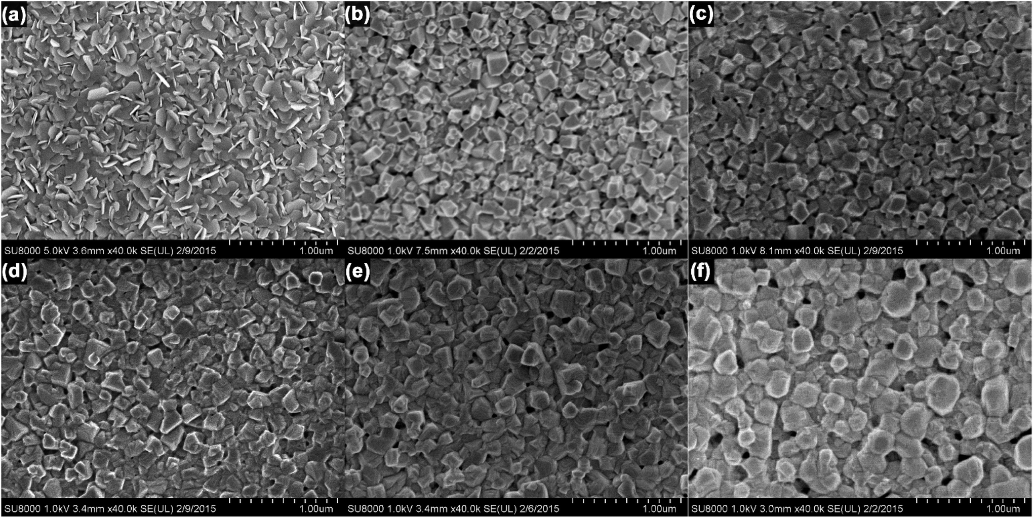 | ||
| Fig. 3 (a) SEM images of (a) PbI2, and CH3NH3PbI3 films prepared at (b) 1%, (c) 20%, (d) 30%, (e) 40%, and (f) 60% RH. | ||
From these analyses, it is evident that the RH has a substantial effect on the growth and crystallization of perovskite films. In the sequential deposition method, the intercalation of CH3NH3I and the formation of CH3NH3PbI3 starts at the surface of the PbI2 crystallites immediately after immersion in the methylammonium iodide solution; however, ion diffusion within the bulk of the PbI2 crystallites is relatively slow, and it takes several minutes for the conversion to CH3NH3PbI3 to complete.37 As a result, drying the film after 3 min is unlikely to result in the formation of well-ordered CH3NH3PbI3 crystals. Additionally, given the insolubility of PbI2 in isopropanol, the extent to which any one CH3NH3PbI3 crystal can grow is limited by the size of its PbI2 precursor. In the absence of other factors, this produces small, poorly crystalline perovskite grains that contain residual PbI2, entirely consistent with the data in Fig. 2c. At this stage, the relative humidity around the perovskite film plays a crucial role in the growth of the crystals. In humid environments, water can be reversibly absorbed into the perovskite film, leading to the formation of hydrate phases.23–27 Ion diffusion in these less compact phases is expected to be more facile; therefore, when the absorbed water eventually leaves the film, it leaves behind a higher quality crystal. This recrystallization process is conceptually similar to the solvent annealing procedures commonly employed in thin films of organic semiconductors.38 Furthermore, the solubility of PbI2 is much higher in water than in isopropanol, and the dissolution and recrystallization of grain edges may lead to the merging of adjacent grains within the film.21 This hypothesis is consistent with the rounding of the crystallite edges, the increase in grain size, and the improved inter-particle connectivity that are observed in Fig. 3f.
Effect of humidity on device performance
After preparing perovskite films at various RH, the samples were removed from the atmospheric bag and assembled into complete devices. P3HT was used as the HTM, and was deposited under ambient laboratory conditions; a thin layer of Ag was then evaporated as the counter-electrode. J–V curves and incident photon-to-current efficiency spectra were measured in a N2-filled glovebox under AM1.5G illumination (Fig. 4). Tabulated device performance parameters are shown in Table 1. The power conversion efficiencies (PCEs) of the highest performance devices, as derived from the J–V curves, were 7.1, 9.0, 11.0, 12.2 and 10.0% for the devices prepared at 1, 20, 30, 40 and 60% RH, respectively. The efficiency of the highest performing device in this study (12.2%) is excellent for devices fabricated using P3HT as the HTM, and is likely limited by the hole mobility of P3HT, not by the quality of the perovskite film.33,39 The increase in PCE with increasing RH can largely be attributed to changes in the film crystallinity and morphology. When the perovskite films are fabricated under dry conditions (1% RH), the films consist of small crystallites with numerous grain boundaries and poor inter-particle connectivity (Fig. 3b). As a result, carrier transport within the film is poor, and the short-circuit current density is low. For the best devices, the Jsc increased from 14.2 mA cm−2 (for the film prepared at 1% RH) to 18.9 mA cm−2 when the film was prepared at 40% RH. Similar trends are observed in the average device performance parameters (Table 1). At the same time, elimination of residual PbI2 and growth in the average crystallite size is expected to reduce the number of trap states within the film, leading to the observed improvements in device fill factor as the RH is increased (Table 1). However, these improvements in film morphology and crystallinity must be balanced against the known issues of moisture-induced perovskite decomposition; devices prepared at 60% RH begin to show a drop in PCE, likely due to the formation of a small amount of either hydrate phases25,26 or PbI2. As a result, the optimum humidity for device fabrication appears to be approximately 40% (±10%). | ||
| Fig. 4 (a) J–V curves of the highest performance devices measured at a scan rate of 0.83 V s−1. (b) IPCE spectra of the same devices. | ||
| RH (%) | V oc (V) | J sc (mA cm−2) | J sc (mA cm−2) from IPCE | FF | PCE (%) | PCE (%) from steady-state data |
|---|---|---|---|---|---|---|
| 1 | 0.88 ± 0.03 | 12 ± 1 (14.2) | 10.4 | 0.44 ± 0.04 | 4.6 ± 0.8 (7.1) | 3.4 |
| 20 | 0.91 ± 0.04 | 13 ± 3 (15.4) | 11.1 | 0.48 ± 0.07 | 6 ± 2 (9.1) | 9.0 |
| 30 | 0.94 ± 0.03 | 15.2 ± 0.5 (16.5) | 15.2 | 0.59 ± 0.05 | 9 ± 1 (11.0) | 10.2 |
| 40 | 0.94 ± 0.03 | 17 ± 1 (18.9) | 17.6 | 0.57 ± 0.04 | 9 ± 2 (12.2) | 11.2 |
| 60 | 0.94 ± 0.01 | 16 ± 1 (17.6) | 17.1 | 0.55 ± 0.02 | 8.2 ± 0.8 (10.0) | 9.3 |
In order to validate the trends in short-circuit current density (and hence PCE), IPCE spectra were measured for the best devices (Fig. 4b). The Jsc values calculated by integrating the product of the AM1.5G photon flux and the IPCE spectra are in reasonable agreement with the Jsc values derived from the J–V curves (Table 1). As expected for devices based on CH3NH3PbI3, all of the devices had broad IPCE spectra that spanned the range of 300 to 800 nm. The IPCE also increased with RH, which is consistent with the observed trends in Jsc. The most significant differences between the spectra, however, are the very pronounced changes in photon-to-current efficiency between 300 and 500 nm. In this wavelength range, the IPCE increases from ca. 30% in the devices prepared at 1% RH to a maximum of ca. 70% for those prepared at 40% RH. Yet despite these pronounced changes in IPCE, the light harvesting efficiency for all of the devices in this range is ca. 95% (assuming a 4% loss due to reflection at the air/glass interface). This implies that the low IPCE for the devices made at low RH is due to charge carrier recombination, rather than transmission losses. Furthermore, due to the extremely high absorption cross-section of CH3NH3PbI3 in this wavelength range, most of these photons are absorbed by a thin perovskite layer at the ZnO/CH3NH3PbI3 interface; this suggests that the recombination losses are most pronounced in this spatial region. Schlipf et al. used grazing incidence small angle X-ray scattering to evaluate the distribution of crystallite sizes within perovskite films prepared via the two-step deposition method.40 Their results suggest that due to strain-induced fracturing of the growing perovskite crystals, smaller crystallites are produced closer to the substrate, with larger grain sizes at the surface of the film. Such a grain size distribution would produce a higher concentration of trap states close to the ZnO interface, and would explain the IPCE losses observed in the blue region of the spectrum (Fig. 4b). This problem would be exacerbated in films prepared at low RH, where the grain sizes are smaller overall, and there is limited opportunity for recrystallization processes to occur. It should be noted that humidity-induced changes to the ZnO charge transfer resistance cannot be ruled out, and may also contribute to the changes in the IPCE spectra. Regardless, it is clear that the relative humidity has a dramatic effect on both perovskite crystal growth and device performance.
Effect of humidity on device hysteresis
One of the major concerns of perovskite solar cells is the hysteresis that is often observed in the J–V curves.16,41–43 In order to quantify the amount of hysteresis in our devices, we measured the J–V curves at slow scan rates in both scan directions: forward bias-to-short circuit (FB-SC) and short circuit-to-forward bias (SC-FB). Fig. 5a shows both J–V curves for the best device made at 40% RH. Comparing the FB-SC scan in Fig. 5a to a faster scan (0.83 V s−1) in the same direction on the same device (Fig. 4a), the Jsc and Voc are similar, but the fill factor is reduced from 65% to 61% in the slower scan. This leads to a slight decrease in the PCE, from 12.2% to 11.3%. Changing the scan direction decreased the PCE further, to 10.0%. Although a relatively small effect, this clearly indicates the presence of hysteresis in the device.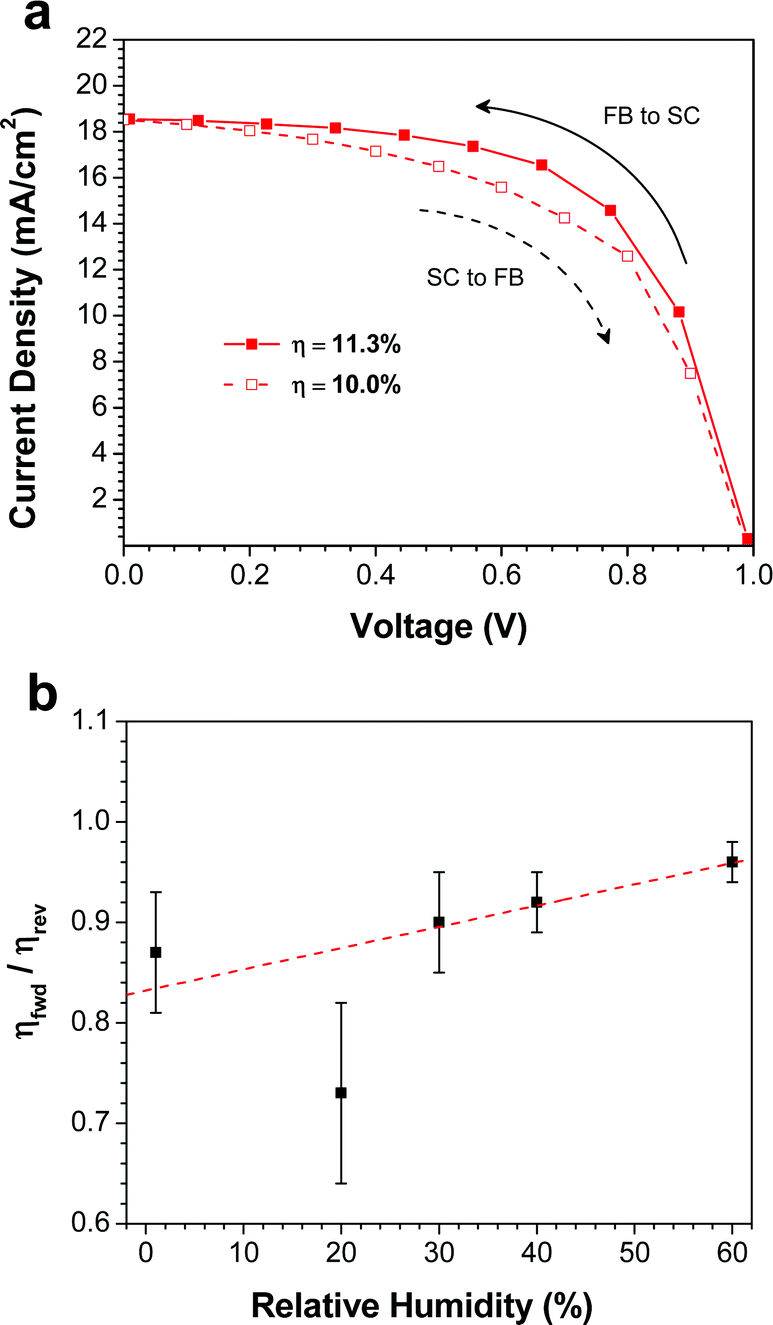 | ||
| Fig. 5 (a) J–V curves measured at 0.1 V s−1 for the best device prepared at 40% RH. (b) Ratio of PCEs determined from forward (SC-FB) and reverse (SC-FB) scans as a function of RH. The linear fit is a guide to the eye. | ||
The J–V curves for the best devices prepared at other RH values are plotted in Fig. S1,† and the ratio of the PCEs measured from the forward (SC-FB) and reverse (FB-SC) scans (ηfwd/ηrev) is plotted as a function of RH (Fig. 5b). The devices fabricated at 1% RH displayed the most pronounced hysteretic behavior. Comparing the fast (Fig. 4a) and slow (Fig. S1a†) scan rates, the device showed a decrease in both Jsc and FF, from 14.2 mA cm−2 and 55% at 0.83 V s−1, to 12.9 mA cm−2 and 50% at 0.1 V s−1, which leads to a decrease in PCE from 7.1% to 5.8%. Upon changing the scan direction at the slower scan rate, the efficiency drops further to 4.8%. As the RH during the film deposition step is increased, the degree of hysteresis in the devices drops substantially (Fig. 5b). For the devices prepared at 60% RH (Fig. S1e†), the average ratio of the efficiencies obtained from forward and reverse scans is 96%, indicating very little dependence of the PCE on scan direction. It has been demonstrated that the hysteresis observed in perovskite solar cells can be caused by several factors: (i) trap states originating from either inherent defects in the perovskite or from grain boundaries,16 or (ii) contact resistance at either the ETM/CH3NH3PbI3 or CH3NH3PbI3/HTM interfaces.43 The hysteresis observed in the devices prepared at low RH is likely caused by the numerous grain boundaries present in the film, which act as charge traps in the device. At higher RH, the increase in the size and connectivity of the crystallites reduces the number of trap states, and in turn a reduction in the device hysteresis is observed.
The average device characteristics as a function of relative humidity are plotted in Fig. 6a. The key trends are an increase in Jsc and FF as the RH is increased, consistent with the elimination of grain boundaries and the crystal growth observed in the perovskite films. In order to further probe the degree of device hysteresis, and to evaluate the device performance under more realistic conditions, we recorded the steady-state power output for representative devices at each RH. The devices were kept at the maximum power point (as determined from the J–V curve) and the photocurrents were recorded as a function of time (Fig. 6b). The stabilized PCE of the device made at 1% RH was found to be 3.4%, whereas it was measured to be 7.1% from the fast scan J–V curve (Fig. 4a). This highlights the large degree of hysteresis observed in the device. For the devices prepared at 20% and above RH, however, the difference between the PCE obtained from the J–V curves and the stabilized power output is more modest (Table 1). The best performing device in the current study (prepared at 40% RH) showed a stabilized PCE of 11.2%, which was much closer to the efficiency calculated from the J–V curve (12.2%); this reinforces the idea that the larger crystallite sizes observed in the perovskite layer lead to a reduction in the amount of device hysteresis.
 | ||
| Fig. 6 (a) Average device performance characteristics (measured at a scan rate of 0.1 V s−1) as a function of relative humidity. Error bars represent plus or minus one standard deviation from the mean. (b) Steady-state current densities for representative devices at each relative humidity. | ||
Conclusion
In conclusion, we prepared perovskite films by the sequential deposition method in a controlled humidity environment. We found an increase in the crystallinity of the perovskite films with increasing RH. At low RH, the films consisted of small cubic crystals with large gaps between them; however, after increasing the RH, larger grains with better inter-particle connectivity were observed. These changes in film crystallinity and morphology have a pronounced effect on device performance, and films prepared at higher RH values produced devices with higher efficiencies and reduced device hysteresis. By carefully controlling the RH, we were able to achieve PCEs of up to 12.2% using P3HT as HTM. These results clearly demonstrate that careful control of all environmental parameters involved in the formation of perovskite films is necessary if reproducible fabrication procedures for perovskite solar cells are to be established.Acknowledgements
The Natural Sciences and Engineering Research Council of Canada (NSERC) and the University of Saskatchewan are acknowledged for financial support. T. L. K. is a Canada Research Chair in Photovoltaics. This research was undertaken, in part, thanks to funding from the Canada Research Chairs program.References
- Q. Dong, Y. Fang, Y. Shao, P. Mulligan, J. Qiu, L. Cao and J. Huang, Science, 2015, 347, 967–970 CrossRef CAS PubMed.
- S. D. Stranks, G. E. Eperon, G. Grancini, C. Menelaou, M. J. P. Alcocer, T. Leijtens, L. M. Herz, A. Petrozza and H. J. Snaith, Science, 2013, 342, 341–344 CrossRef CAS PubMed.
- G. Xing, N. Mathews, S. Sun, S. S. Lim, Y. M. Lam, M. Gratzel, S. Mhaisalkar and T. C. Sum, Science, 2013, 342, 344–347 CrossRef CAS PubMed.
- D. Shi, V. Adinolfi, R. Comin, M. Yuan, E. Alarousu, A. Buin, Y. Chen, S. Hoogland, A. Rothenberger, K. Katsiev, Y. Losovyj, X. Zhang, P. A. Dowben, O. F. Mohammed, E. H. Sargent and O. M. Bakr, Science, 2015, 347, 519–522 CrossRef CAS PubMed.
- A. Kojima, K. Teshima, Y. Shirai and T. Miyasaka, J. Am. Chem. Soc., 2009, 131, 6050–6051 CrossRef CAS PubMed.
- H. Zhou, Q. Chen, G. Li, S. Luo, T.-B. Song, H.-S. Duan, Z. Hong, J. You, Y. Liu and Y. Yang, Science, 2014, 345, 542–546 CrossRef CAS PubMed.
- D. Liu and T. L. Kelly, Nat. Photonics, 2014, 8, 133–138 CrossRef CAS.
- J. Burschka, N. Pellet, S.-J. Moon, R. Humphry-Baker, P. Gao, M. K. Nazeeruddin and M. Gratzel, Nature, 2013, 499, 316–319 CrossRef CAS PubMed.
- M. Liu, M. B. Johnston and H. J. Snaith, Nature, 2013, 501, 395–398 CrossRef CAS PubMed.
- M. M. Lee, J. Teuscher, T. Miyasaka, T. N. Murakami and H. J. Snaith, Science, 2012, 338, 643–647 CrossRef CAS PubMed.
- W. Nie, H. Tsai, R. Asadpour, J.-C. Blancon, A. J. Neukirch, G. Gupta, J. J. Crochet, M. Chhowalla, S. Tretiak, M. A. Alam, H.-L. Wang and A. D. Mohite, Science, 2015, 347, 522–525 CrossRef CAS PubMed.
- J.-H. Im, I.-H. Jang, N. Pellet, M. Grätzel and N.-G. Park, Nat. Nanotechnol., 2014, 9, 927–932 CrossRef CAS PubMed.
- N. J. Jeon, J. H. Noh, Y. C. Kim, W. S. Yang, S. Ryu and S. I. Seok, Nat. Mater., 2014, 13, 897–903 CrossRef CAS PubMed.
- M. A. Green, K. Emery, Y. Hishikawa, W. Warta and E. D. Dunlop, Prog. Photovoltaics: Res. Appl., 2015, 23, 1–9 CrossRef.
- S. D. Stranks, P. K. Nayak, W. Zhang, T. Stergiopoulos and H. J. Snaith, Angew. Chem., Int. Ed., 2015, 54, 3240–3248 CrossRef CAS PubMed.
- Y. Shao, Z. Xiao, C. Bi, Y. Yuan and J. Huang, Nat. Commun., 2014, 5, 5784 CrossRef CAS PubMed.
- W. Zhang, M. Saliba, D. T. Moore, S. K. Pathak, M. T. Hörantner, T. Stergiopoulos, S. D. Stranks, G. E. Eperon, J. A. Alexander-Webber, A. Abate, A. Sadhanala, S. Yao, Y. Chen, R. H. Friend, L. A. Estroff, U. Wiesner and H. J. Snaith, Nat. Commun., 2015, 6, 6142 CrossRef CAS PubMed.
- S. T. Williams, F. Zuo, C.-C. Chueh, C.-Y. Liao, P.-W. Liang and A. K. Y. Jen, ACS Nano, 2014, 8, 10640–10654 CrossRef CAS PubMed.
- S. Colella, E. Mosconi, P. Fedeli, A. Listorti, F. Gazza, F. Orlandi, P. Ferro, T. Besagni, A. Rizzo, G. Calestani, G. Gigli, F. De Angelis and R. Mosca, Chem. Mater., 2013, 25, 4613–4618 CrossRef CAS.
- P.-W. Liang, C.-Y. Liao, C.-C. Chueh, F. Zuo, S. T. Williams, X.-K. Xin, J. Lin and A. K. Y. Jen, Adv. Mater., 2014, 26, 3748–3754 CrossRef CAS PubMed.
- J. You, Y. Yang, Z. Hong, T.-B. Song, L. Meng, Y. Liu, C. Jiang, H. Zhou, W.-H. Chang and G. Li, Appl. Phys. Lett., 2014, 105, 183902 CrossRef.
- Z. Xiao, Q. Dong, C. Bi, Y. Shao, Y. Yuan and J. Huang, Adv. Mater., 2014, 26, 6503–6509 CrossRef CAS PubMed.
- B. R. Vincent, K. N. Robertson, T. S. Cameron and O. Knop, Can. J. Chem., 1987, 65, 1042–1046 CrossRef CAS.
- F. Hao, C. C. Stoumpos, Z. Liu, R. P. H. Chang and M. G. Kanatzidis, J. Am. Chem. Soc., 2014, 136, 16411–16419 CrossRef CAS PubMed.
- J. Yang, B. D. Siempelkamp, D. Liu and T. L. Kelly, ACS Nano, 2015, 9, 1955–1963 CrossRef CAS PubMed.
- J. A. Christians, P. A. Miranda Herrera and P. V. Kamat, J. Am. Chem. Soc., 2015, 137, 1530–1538 CrossRef CAS PubMed.
- A. M. A. Leguy, Y. Hu, M. Campoy-Quiles, M. I. Alonso, O. J. Weber, P. Azarhoosh, M. van Schilfgaarde, M. T. Weller, T. Bein, J. Nelson, P. Docampo and P. R. F. Barnes, Chem. Mater., 2015, 3397–3407 CrossRef CAS.
- K. K. Bass, R. E. McAnally, S. Zhou, P. I. Djurovich, M. E. Thompson and B. C. Melot, Chem. Commun., 2014, 50, 15819–15822 RSC.
- H. Gao, C. Bao, F. Li, T. Yu, J. Yang, W. Zhu, X. Zhou, G. Fu and Z. Zou, ACS Appl. Mater. Interfaces, 2015, 9110–9117 CAS.
- N. Yantara, D. Sabba, F. Yanan, J. M. Kadro, T. Moehl, P. P. Boix, S. Mhaisalkar, M. Gratzel and C. Gratzel, Chem. Commun., 2015, 51, 4603–4606 RSC.
- K. Liang, D. B. Mitzi and M. T. Prikas, Chem. Mater., 1998, 10, 403–411 CrossRef CAS.
- J. H. Im, C. R. Lee, J. W. Lee, S. W. Park and N. G. Park, Nanoscale, 2011, 3, 4088–4093 RSC.
- D. Liu, M. K. Gangishetty and T. L. Kelly, J. Mater. Chem. A, 2014, 2, 19873–19881 CAS.
- S. De Wolf, J. Holovsky, S.-J. Moon, P. Löper, B. Niesen, M. Ledinsky, F.-J. Haug, J.-H. Yum and C. Ballif, J. Phys. Chem. Lett., 2014, 5, 1035–1039 CrossRef CAS PubMed.
- J. Kim, S.-H. Lee, J. H. Lee and K.-H. Hong, J. Phys. Chem. Lett., 2014, 5, 1312–1317 CrossRef CAS PubMed.
- C. C. Stoumpos, C. D. Malliakas and M. G. Kanatzidis, Inorg. Chem., 2013, 52, 9019–9038 CrossRef CAS PubMed.
- Y. Wu, A. Islam, X. Yang, C. Qin, J. Liu, K. Zhang, W. Peng and L. Han, Energy Environ. Sci., 2014, 7, 2934–2938 CAS.
- K. C. Dickey, J. E. Anthony and Y. L. Loo, Adv. Mater., 2006, 18, 1721–1726 CrossRef CAS.
- J. Xiao, J. Shi, H. Liu, Y. Xu, S. Lv, Y. Luo, D. Li, Q. Meng and Y. Li, Adv. Energy Mater., 2015, 5, 1401943 Search PubMed.
- J. Schlipf, P. Docampo, C. J. Schaffer, V. Körstgens, L. Bießmann, F. Hanusch, N. Giesbrecht, S. Bernstorff, T. Bein and P. Müller-Buschbaum, J. Phys. Chem. Lett., 2015, 6, 1265–1269 CrossRef CAS PubMed.
- E. L. Unger, E. T. Hoke, C. D. Bailie, W. H. Nguyen, A. R. Bowring, T. Heumuller, M. G. Christoforo and M. D. McGehee, Energy Environ. Sci., 2014, 7, 3690–3698 CAS.
- H.-S. Kim and N.-G. Park, J. Phys. Chem. Lett., 2014, 5, 2927–2934 CrossRef CAS PubMed.
- H. J. Snaith, A. Abate, J. M. Ball, G. E. Eperon, T. Leijtens, N. K. Noel, S. D. Stranks, J. T.-W. Wang, K. Wojciechowski and W. Zhang, J. Phys. Chem. Lett., 2014, 5, 1511–1515 CrossRef CAS PubMed.
Footnote |
| † Electronic supplementary information (ESI) available: J–V curves in both scan directions for representative devices prepared at each RH. See DOI: 10.1039/c5nr04179a |
| This journal is © The Royal Society of Chemistry 2016 |