
 Open Access Article
 This Open Access Article is licensed under a
 Creative Commons Attribution 3.0 Unported Licence
Structural differences between Sb- and Nb-doped tin oxides and consequences for electrical conductivity†
Emma
Oakton
a,
Jérémy
Tillier
b,
Georges
Siddiqi
a,
Zlatko
Mickovic
b,
Olha
Sereda
b,
Alexey
Fedorov
a and
Christophe
Copéret
*a
aETH Zürich, Department of Chemistry and Applied Biosciences, Vladimir Prelog Weg 1–5, CH-8093 Zürich, Switzerland. E-mail: ccoperet@inorg.chem.ethz.ch; Fax: +41 44 633 1325; Tel: +41 44 633 9394
bCSEM SA, XRD Application Lab & Microscopy, Jaquet-Droz 1, CH-2002, Neuchâtel, Switzerland
First published on 25th January 2016
Abstract
Sb- and Nb-doped tin oxides have been prepared by a co-precipitation method. Whilst X-ray powder diffraction and EDX mapping indicate similar dopant distributions, more detailed characterisation by variable high-temperature XRD, 119Sn MAS NMR and Nb K-edge X-ray absorption near edge structure spectroscopy reveal clear differences in the oxide structures. This detailed structural information is used to validate the measured differences in electrical conductivity.
Introduction
Tin-based metal oxides1 have a highly diverse range of applications including gas sensor technology,2–5 lithium ion batteries,6–8 optoelectronic devices,9–11 Polymer Electrolyte Fuel Cells (PEFCs)12–14 and heterogeneous catalysis.15,16 The performance of tin oxide in many of these applications depends on the tuning of its electrical conductivity. While pure stoichiometric SnO2 is an insulator, the addition of a dopant atom can increase carrier concentrations and electron mobility, thereby enhancing electrical conductivity.17 For instance the incorporation of Sb, a group (V) electron donor, into the host SnO2 lattice provides antimony-doped tin oxide (ATO), which is a well known electron conductor18–20 with numerous applications.9,21–24 The high conductivity of ATO has lead to its investigation as a carbon-free durable catalyst support for PEFCs.25–29 However, recent studies have shown that the activity and durability of ATO in electrochemical systems is highly dependant on the surface concentration of Sb.25 Currently, the search for stable materials with high electrical conductivity continues to be of high importance for the further development of PEFC technology.30Niobium-doped tin oxide has been investigated as an alternative to ATO under PEFC relevant conditions.14,31 Increased Electrochemically Active Surface Area (ECSA) and mass activity were reported for Nb-doped tin oxide, despite its lower electrical conductivity in comparison to ATO.32 Interestingly, there is a wide variety of reported electrical conductivity values for Nb-doped SnO2 aimed towards PEFC applications,14,32–38 ranging between 1600 and 0.07 S cm−1 for thin films33–35,37 and from 0.02 to 1.1 × 10⁻⁴ S cm−1 for high surface area nanopowders.14,32,36 Indeed it is known that electrical conductivity can vary as a function of the amount of dopant and the homogeneity of its distribution within the host oxide lattice, the latter depends greatly on the preparation method. As there is a wide range of methods for the preparation of doped oxides, detailed characterisation is vital to fully understand the material's structure–property relationship.
In this work we present the preparation of high surface area Sb- and Nb-doped tin oxides by an aqueous co-precipitation method, similar protocols of which have been used for the preparation of doped tin oxides.39–42 Characterisation by variable high-temperature X-ray diffraction, 119Sn NMR spectroscopy and Nb K-edge X-ray absorption near edge structure spectroscopy reveal key structural differences, which provide clues to the origin of the measured electrical conductivity.
Results and discussion
Preparation and characterisation of Sb-doped tin oxide
Antimony-doped tin oxide (SnO2:Sb) was prepared by a co-precipitation route, where increasing the pH of an aqueous solution of SbCl5 and SnCl4 triggers oxide precipitation. The resulting material was calcined under air flow at 500 °C prior to analysis. Elemental analysis revealed the Sb loading to be approximately half that of the nominal loading (2.5 and 5 mol% respectively, Table S1, ESI†). The electrical conductivity of SnO2:Sb was 0.02 S cm−1, determined from 4-point direct current measurement, which is comparable to commercially available ATO (Table S2, ESI†). TEM imaging indicates this material has a nanoparticulate structure with particle diameters between 4–8 nm (Fig. S1, ESI†). The type II nitrogen adsorption–desorption isotherm is typical of all materials reported here (vide infra) and indicates a macroporous structure, likely due to inter-particle space (Fig. S4, ESI†). Analysis with BET theory gave a surface area of 83 m2 g−1 (Table S1, ESI†). Furthermore, EDX mapping shows an even distribution of Sb (Fig. S2 and S3, ESI†). Detailed HT-XRD studies43–45 showed that cassiterite SnO2 is the only phase present in SnO2:Sb (Fig. S3, ESI†). Next, in situ HT-XRD measurements were used to compare the crystallisation process of SnO2:Sb to SnO2 prepared by the same method. For each sample, Bragg–Brentano diffraction patterns were acquired under ambient atmosphere at 50 °C intervals between 100 and 800 °C and analysed using Rietveld refinement. The temperature dependence of lattice volume and crystallite size for both samples is shown in Fig. 1a. The non-linear evolution of lattice volume during the first heating cycle shows an initial decrease, which indicates an improvement in chemical order, likely due to increasing crystallinity along with condensation of surface groups.46 An increase in lattice volume, associated with thermal expansion, is observed above 500 °C and during the second heating cycle. Fig. 1b reveals that the crystallite size increases rapidly from 500 °C and continues to increase up to 800 °C, suggesting that crystallisation continues after hydroxyl condensation. These results show that both samples have a similar rate of lattice volume contraction during the first cycle of annealing and reach comparable crystallite sizes. This behavioural similarity is an indication that Sb is doped within the SnO2 lattice, as segregated dopant phases have been reported to hinder SnO2 particle growth.46,47 Moreover there is a significant decrease in the lattice volume of SnO2:Sb in comparison to SnO2, which indicates antimony is within the SnO2 lattice, due to the smaller ionic radium of Sb5+ in comparison to Sn4+.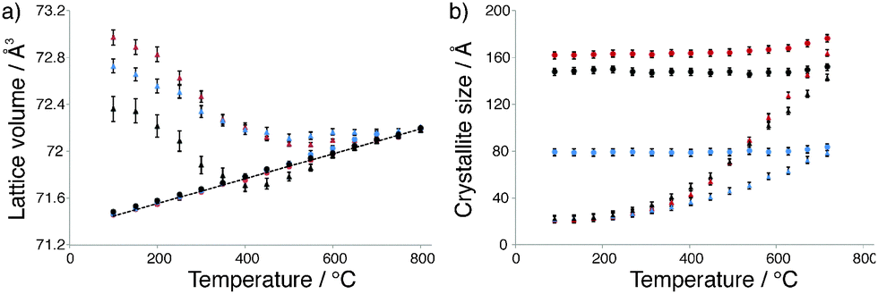 | ||
| Fig. 1 (a) Variation of lattice volume and (b) crystallite size with temperature for SnO2 (red), SnO2:Sb (black) and SnO2:Nb (blue). | ||
119Sn MAS NMR spectroscopy was used to compare the Sn(IV) environment in SnO2:Sb and SnO2 before and after calcination (Fig. 2). Both as-synthesised samples have a peak at −602 ppm with similar line shape and width, which indicates Sn(IV) centres are in the same chemical environment. This could be explained either by the presence of segregated SnO2 and Sb2O5 phases or low crystallinity. Indeed the latter would be consistent with smaller lattice volume observed even at low temperatures (vide supra). After calcination, the Sn(IV) signal of SnO2 narrows significantly due to crystallisation and particle growth, as confirmed by XRD and TEM (Fig. S1 and S3, ESI†). However, despite a similar morphological change, the Sb doped sample shows line broadening, consistent with the presence of a dopant within SnO2 lattice.48,49
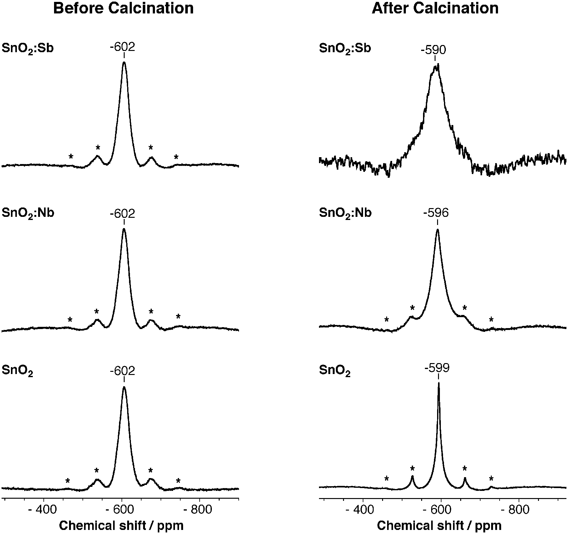 | ||
| Fig. 2 119Sn MAS NMR spectra of SnO2, SnO2:Sb and SnO2:Nb before and after calcination at 500 °C. Asterisks denote spinning side bands. | ||
Preparation and characterisation of Nb-doped tin oxide
Having shown that this co-precipitation method is viable for the preparation of SnO2:Sb with high surface area and high electrical conductivity, the preparation of niobium-doped tin oxide (SnO2:Nb) was explored. As the dopant concentration can have a large influence on electrical conductivity, we initially varied Nb content between 0 and 10 molM%, where molM refers to the nominal moles of metal atoms. All samples were calcined at 500 °C prior to characterisation. The surface areas and nanoparticle sizes of all prepared SnO2:Nb materials are comparable (Table S3, ESI†). Nb content has little influence on the electrical conductivity with only a small increase noted for the 5.1 nominal molM% Nb-doped sample (Table S3, ESI†).Therefore this SnO2:Nb sample (5.1 molM% Nb by elemental analysis) was selected to investigate the effects of post-synthetic treatment. Assessing several calcination temperatures in the range of 350 °C to 800 °C increased sample crystallinity shown by XRD (Fig. S3, ESI†). Electronic conductivity was slightly improved for the calcined samples and calcination at 500 °C gave the highest value 10−5 S cm−1 (Table S4, ESI†), which was still much lower than that of SnO2:Sb.
In order to rationalise the low electrical conductivity of SnO2:Nb, it is necessary to have a better understanding of its structure. Firstly it is important to note that TEM imaging shows similar morphology for SnO2:Nb in comparison to SnO2:Sb and SnO2 (Fig. S1, ESI†). The XRD powder diffraction pattern of as-synthesised SnO2:Nb fits with that of cassiterite SnO2 (Fig. S3, ESI†). HT-XRD measurements were used to compare the crystallisation behaviour of SnO2:Nb with SnO2 and SnO2:Sb described above (Fig. 1). The slightly slower rate of lattice volume contraction for the Nb doped material indicates that the chemical order improvement is impeded. Additionally, the crystallite size of SnO2:Nb increases at a slower rate in comparison to SnO2 and SnO2:Sb and the size reached at 800 °C is approximately half the size of SnO2 (80 Å vs. 160 Å). This could be due to the presence of segregated Nb2O5 hindering the growth of nanoparticles.46,47 This XRD study suggests that the Nb dopant is fully or partially segregated and forms small XRD silent crystallites, likely Nb2O5.
To further investigate the possible segregation of Nb2O5, 119Sn MAS NMR was used to compare the samples before and after calcination at 500 °C (Fig. 2). Both as-synthesised SnO2 and SnO2:Nb have a single peak at −602 ppm which is assigned to Sn(IV) centres. The similarity of peak position and shape suggests that the Sn(IV) sites are in similar chemical environments. Similarly to SnO2:Sb, the Sn(IV) signal of SnO2:Nb broadens after calcination, indicating an increasing variety of Sn(IV) chemical environments introduced by the dopant.48,49 In accordance with the HT-XRD investigation, these results support the partial segregation of the Nb dopant.
In addition to changes in line shape, a downfield shift is observed in the 119Sn MAS NMR spectra for all calcined materials, with SnO2:Sb having the largest shift and SnO2 having the smallest. Such changes in chemical shift have been previously associated with the formation of oxygen defects, which reduces electron density around the analyte atom.49 The presence of oxygen defects is supported by EPR measurements (Fig. 3). Paramagnetic species are not observed before calcination. After calcination, two signals are observed for SnO2 at g = 2 (sharp), assigned to superoxide species and/or oxygen defects50 and at g = 1.89 (broad), which is assigned to oxygen defects.51 For calcined SnO2:Nb a single broad signal at g = 1.89 is recorded and is attributed to oxygen defects with weak hyperfine coupling likely due to interaction with Nb. This weak defect-Nb interaction suggests that Nb is in close proximity to the vacancies, likely in the SnO2 lattice. The absence of EPR signal for calcined SnO2:Sb is likely due to its high electron conductivity, causing fast signal relaxation.
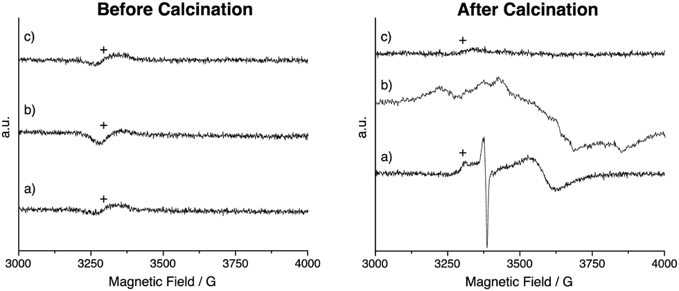 | ||
| Fig. 3 EPR spectra of (a) SnO2, (b) SnO2:Nb and (c) SnO2:Sb before and after calcination. Signal due to the EPR cavity is denoted by +. | ||
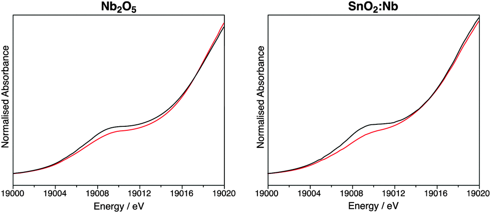
Thus far, the characterisation techniques used have focussed on comparisons of lattice dimensions and the Sn environment. However it is also important to characterise the dopant environment. X-ray absorption near edge spectroscopy (XANES) was used to characterise SnO2:Nb from the Nb point of view and compare it to Nb2O5, prepared by the same precipitation method, as well as to commercial Nb2O5. Fig. 4 shows the Nb K-edge XANES for these three oxides before and after calcination. The position of the edge is indicative of oxidation state, and all samples before and after calcination have a near identical edge position to the Nb2O5 standard, indicating the oxidation state of Nb is +5. The pre-edge feature at ca. 18994 eV is indicative of the tetrahedral geometry around Nb, and its absence is typical of an octahedral Nb environment.52 All samples exhibit this pre-edge feature, suggesting all contain tetrahedral Nb as in Nb2O5.53Fig. 5 shows the overlapped spectra for Nb2O5 (prepared by precipitation) and SnO2:Nb. The calcination treatment results in a decrease in the pre-edge feature for both samples, indicating a shift from tetrahedral to octahedral geometry. In the case of Nb2O5, this is likely due to the crystallisation process. However the more pronounced tetrahedral to octahedral shift observed for SnO2:Nb indicates that an additional process may be occurring. Such a change in geometry would also be consistent with the migration of Nb5+ centres into the SnO2 lattice to occupy octahedral Sn4+ sites.
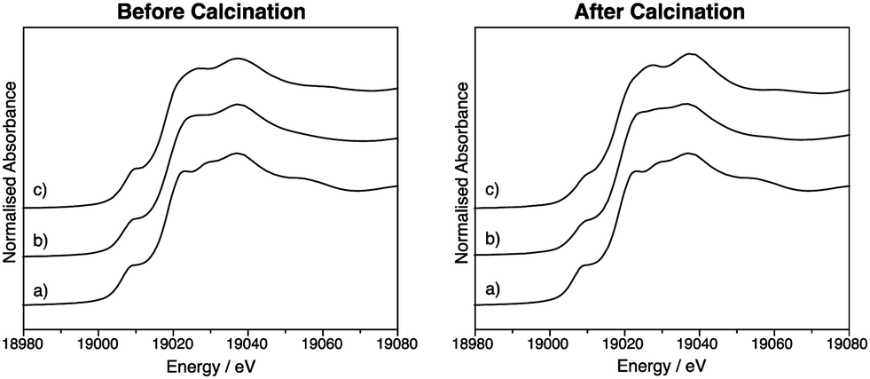 | ||
| Fig. 4 Nb-K edge XANES data for (a) commercial Nb2O5, (b) Nb2O5 and (c) SnO2:Nb before and after calcination. | ||
 | ||
| Fig. 5 Nb-K edge XANES data comparison for Nb2O5 and SnO2:Nb before (black) and after (red) calcination. | ||
This analysis is consistent with the XRD and NMR results, suggesting the as-synthesised material is composed of SnO2 and Nb2O5 domains. Upon calcination to 500 °C, Nb partially migrates into the SnO2 lattice leaving small Nb2O5 crystallites, which are not detected by XRD.
Conclusions
Herein we have described a co-precipitation method for the preparation of high surface area conductive ATO, similar to materials available commercially. Characterisation by HT-XRD and 119Sn MAS NMR indicate that Sb is homogeneously distributed within the SnO2 lattice. In contrast, SnO2:Nb prepared by the same method has low conductivity and varying both Nb content and calcination temperature yields only a negligible improvement in electrical conductivity. Characterisation by HT-XRD shows that the Nb dopant is most likely present in a XRD-silent Nb2O5 domain. This interpretation is supported by Nb K-edge XANES measurements, which additionally show that Nb is partially migrating into SnO2 during the calcination treatment. This is further confirmed by 119Sn MAS NMR spectroscopy. Our data suggests that the low conductivity of these SnO2:Nb materials is due to the inhomogeneous doping of Nb in SnO2. This investigation exemplifies that it is essential to characterise doped oxides by a combination of techniques from both the host and dopant point of view in order to fully understand the material structure. Through this investigation we have revealed significant structural differences between Sb and Nb doped SnO2, despite their preparation by an analogous co-precipitation method and their apparent similar structure according to classical characterisation techniques such as XRD diffraction and EDX mapping. We are now using this information and these combined techniques to develop an alternative approach to the synthesis of homogeneously Nb-doped tin oxide.Experimental
General
SnCl4·5H2O (98%), SbCl5 (99.999%), concentrated hydrochloric acid (99%), ammonium hydroxide (25% NH3) and absolute ethanol were purchased from Sigma Aldrich and used as received. NbCl5 (99.99%) was purchased from Strem Chemicals. Commercial ATO and Nb2O5 were obtained from Mitsubishi and Acros Organics respectively. Distilled water was further purified using a Merck Millipore Synergy Ultrapure Water System and had a resistivity of 18.2 MΩ cm at 25 °C. N2 adsorption–desorption analysis was conducted using a BEL-Mini device supplied by BEL Japan Inc. All samples were pre-treated at 150 °C under vacuum for 16 h on a BEL-Prep machine also from BEL Japan Inc. Results were fitted using BEL-Master programme and BET theory. Bright Field TEM images were recorded using a 100 kV Philips CM12 transmission electron microscope. EDX maps were conducted on a FEI Talos F200X microscope. Electrical conductivity values were determined at room temperature from powder disks under 0.625 MPa pressure with thicknesses in the range 100–1000 μm and averaged to give the reported values. For pure SnO2 and SnO2:Nb samples conductivity values were determined using 4-point Electrical Impedance Spectroscopy. For SnO2:Sb, DC measurements were used, where the current was recorded for a range of voltages (0.001–0.1 V) and conductivity subsequently calculated using Ohm's law. 119Sn MAS NMR measurements were conducted on a 400 MHz Bruker spectrometer at 10 kHz spinning speed; the samples were packed in a 4 mm zirconia rotor. For all samples 7168 scans were recorded, except for calcined SnO2:Sb where 14336 scans were acquired. Continuous Wave (CW) EPR spectra of the powders in quartz tubes were recorded on a Bruker EMX X-Band spectrometer (9.5 GHz microwave frequency) at 110 K. XANES measurements at Nb K-edge were performed at the SuperXAS beamline at the Swiss Light Source (Paul Scherrer Institute, Villigen, Switzerland). The SLS is a third generation synchrotron, which operates under top up mode, 2.4 GeV electron energy, and a current of 400 mA. The SuperXAS beamline is positioned on one of three super-bent ports. The incident beam was collimated by Si-coated mirror at 2.8 mrad, monochromatized using a double crystal Si(111) monochromator, and focused with Rh coated toroidal mirror (at 2.8 mrad) down to 100 × 100 μm. The beam intensity was of 4–5 × 10¹¹ ph s−1.XRD characterisation
The high-temperature X-ray diffraction (HT-XRD) experiments were performed using an Anton Paar HTK 16N high-temperature chamber mounted in an X'Pert Pro-MPD diffractometer. The samples were deposited on top of the Pt heating strip as a slurry in EtOH and allowed to dry. To ensure accurate temperature control the temperature regulator was attached onto the Pt strip. The samples were heated from room temperature up to 800 °C with a heating-rate of 2 °C min−1 under ambient atmosphere. Bragg–Brentano diffraction patterns were acquired at 50 °C intervals between 100 °C to 800 °C. For each temperature step, a stabilisation time of 5 minutes was allowed before acquisition. After the first in situ annealing, the samples were cooled down to room temperature with a cooling-rate of 60 °C min−1 and a second HT-XRD experiment was then performed under the same conditions. The diffractometer was equipped with the copper Kα radiation (1.541874 Å) and the diffracted intensity has been recorded using a PIXcel detector with its maximum active length of 3.347° in order to allow quick acquisition of each diffractogram. The diffraction patterns have been acquired for 2θ angles ranging from 20 to 90° with a step size of 0.1°. Instrumental broadening of XRD peaks has been taken in account using the NIST 674b standard. In case of the lattice volume, the values of error bars were calculated based on the deviations of the structure model used to determine lattice constants. The propagation of errors in lattice volume calculation was taken in account. In case of crystallite size, we fixed the error to ±3 Å, which corresponds to the reproducibility error of crystallite size determination.Preparation of SnO2
SnCl4·5H2O (16 g, 0.046 mol) was dissolved in 250 mL distilled H2O. NH4OH was added until the solution reached pH = 3, after which a white precipitate was formed. After stirring for 1 h, the precipitate was washed with distilled water and EtOH. After drying on a rotary evaporator (40 °C, 100 mbar), the white solid was dried under air flow at 80 °C for 1 h.Preparation of SnO2:Sb
SnCl4·5H2O (15 g, 0.043 mol) was dissolved in 250 mL distilled H2O. SbCl5 (0.71 g, 2.4 × 10⁻³ mol) was immediately dissolved in conc. HCl (2 mL) and added to the Sn chloride solution. Following steps were conducted as described for SnO2.Representative preparation of 5 molM% SnO2:Nb
SnCl4·5H2O (15 g, 0.043 mol) was dissolved in 250 mL distilled H2O. NbCl5 (0.62 g, 2.3 × 10⁻³ mol) was removed from an Ar filled glovebox, immediately dissolved in conc. HCl (2 mL) and added to the Sn chloride solution. Following steps were conducted as described for SnO2.Preparation of Nb2O5
NbCl5 (3.95 g, 0.015 mol) was removed from an Ar filled glovebox, immediately dissolved in conc. HCl (6 mL) and added to ultrapure water (100 mL). Following steps were conducted as described for SnO2.Calcination treatments
Approximately 2 g of the as-synthesised material was loaded into a glass flow reactor and calcined under synthetic air (120 mL min−1). All samples were calcined at 500 °C for 16 h (120 °C min−1) and cooled under air flow. SnO2:Nb was calcined at additional temperatures of 350, 650 and 800 °C.Acknowledgements
This research was supported by CCEM Switzerland and Umicore AG & Co. KG (project DuraCAT). The authors would like to acknowledge the group of T. J. Schmidt (PSI Villigen, Switzerland) for insightful discussions and access to electrical conductivity set up. Frank Krumeich is thanked for performing the EDX maps along with ScopeM at ETH Zürich for the use of their electron microscopy facilities.Notes and references
- M. Batzill and U. Diebold, Prog. Surf. Sci., 2005, 79, 47–154 CrossRef CAS.
- G. Zhang and M. Liu, Sens. Actuators, B, 2000, 69, 144–152 CrossRef CAS.
- J. Watson, Sens. Actuators, 1984, 5, 29–42 CrossRef CAS.
- C. Nayral, T. Ould-Ely, A. Maisonnat, B. Chaudret, P. Fau, L. Lescouzeres and A. Peyre-Lavigne, Adv. Mater., 1999, 11, 61–63 CrossRef CAS.
- A. Kolmakov, Y. X. Zhang, G. S. Cheng and M. Moskovits, Adv. Mater., 2003, 15, 997–1000 CrossRef CAS.
- H. B. Wu, J. S. Chen, H. H. Hng and X. W. Lou, Nanoscale, 2012, 4, 2526–2542 RSC.
- Y. L. Zhang, Y. Liu and M. L. Liu, Chem. Mater., 2006, 18, 4643–4646 CrossRef CAS.
- Y. Idota, T. Kubota, A. Matsufuji, Y. Maekawa and T. Miyasaka, Science, 1997, 276, 1395–1397 CrossRef CAS.
- I. Saadeddin, B. Pecquenard, J. P. Manaud, R. Decourt, C. Labrugere, T. Buffeteau and G. Campet, Appl. Surf. Sci., 2007, 253, 5240–5249 CrossRef CAS.
- Z. R. Dai, Z. W. Pan and Z. L. Wang, Adv. Funct. Mater., 2003, 13, 9–24 CrossRef CAS.
- C. A. Hoel, T. O. Mason, J. F. Gaillard and K. R. Poeppelmeier, Chem. Mater., 2010, 22, 3569–3579 CrossRef CAS.
- T. Takeguchi, Y. Anzai, R. Kikuchi, K. Eguchi and W. Ueda, J. Electrochem. Soc., 2007, 154, B1132–B1137 CrossRef CAS.
- A. Masao, S. Noda, F. Takasaki, K. Ito and K. Sasaki, Electrochem. Solid-State Lett., 2009, 12, B119–B122 CrossRef CAS.
- T. Tsukatsune, Y. Takabatake, Z. Noda, T. Daio, A. Zaitsu, S. M. Lyth, A. Hayashi and K. Sasaki, J. Electrochem. Soc., 2014, 161, F1208–F1213 CrossRef.
- A. Hagemeyer, Z. Hogan, M. Schlichter, B. Smaka, G. Streukens, H. Turner, A. Volpe, H. Weinberg and K. Yaccato, Appl. Catal., A, 2007, 317, 139–148 CrossRef CAS.
- X. Xu, R. Zhang, X. Zeng, X. Han, Y. Li, Y. Liu and X. Wang, ChemCatChem, 2013, 5, 2025–2036 CrossRef CAS.
- Z. C. Orel, B. Orel, M. Hodoscek and V. Kaucic, J. Mater. Sci., 1992, 27, 313–318 CrossRef CAS.
- E. Shanthi, V. Dutta, A. Banerjee and K. L. Chopra, J. Appl. Phys., 1980, 51, 6243–6251 CrossRef CAS.
- K. C. Mishra, K. H. Johnson and P. C. Schmidt, Phys. Rev. B: Condens. Matter Mater. Phys., 1995, 51, 13972–13976 CrossRef CAS.
- D. R. Leite, I. O. Mazali, E. C. Aguiar, W. C. Las and M. Cilense, J. Mater. Sci., 2006, 41, 6256–6259 CrossRef CAS.
- Y. D. Wang, I. Djerdj, M. Antonietti and B. Smarsly, Small, 2008, 4, 1656–1660 CrossRef CAS PubMed.
- Y. D. Wang, Q. Y. Mu, G. F. Wang and Z. L. Zhou, Sens. Actuators, B, 2010, 145, 847–853 CrossRef CAS.
- L. Luo, D. Bozyigit, V. Wood and M. Niederberger, Chem. Mater., 2013, 25, 4901–4907 CrossRef CAS.
- V. Muller, M. Rasp, J. Rathousky, B. Schutz, M. Niederberger and D. Fattakhova-Rohlfing, Small, 2010, 6, 633–637 CrossRef PubMed.
- E. Fabbri, A. Rabis, R. Kotz and T. J. Schmidt, Phys. Chem. Chem. Phys., 2014, 16, 13672–13681 RSC.
- M. Yin, J. Y. Xu, Q. F. Li, J. O. Jensen, Y. J. Huang, L. N. Cleeman, N. J. Bjerrum and W. Xing, Appl. Catal., B, 2014, 144, 112–120 CrossRef CAS.
- K. Kakinuma, M. Uchida, T. Kamino, H. Uchida and M. Watanabe, Electrochim. Acta, 2011, 56, 2881–2887 CrossRef CAS.
- K. Sasaki, F. Takasaki, Z. Noda, S. Hayashi, Y. Shiratori and K. Ito, ECS Trans., 2010, 33, 473–482 CAS.
- M. L. Dou, M. Hou, F. Wang, D. Liang, Q. Zhao, Z. G. Shao and B. L. Yi, J. Electrochem. Soc., 2014, 161, F1231–F1236 CrossRef.
- A. Rabis, P. Rodriquez and T. J. Schmidt, ACS Catal., 2012, 2, 864–890 CrossRef CAS.
- Y. Senoo, K. Kakinuma, M. Uchida, H. Uchida, S. Deki and M. Watanabe, RSC Adv., 2014, 4, 32180–32188 RSC.
- F. Takasaki, S. Matsuie, Y. Takabatake, Z. Noda, A. Hayashi, Y. Shiratori, K. Ito and K. Sasaki, J. Electrochem. Soc., 2011, 158, B1270–B1275 CrossRef CAS.
- Y. Wang, T. Brezesinski, M. Antonietti and B. Smarsly, ACS Nano, 2009, 3, 1373–1378 CrossRef CAS PubMed.
- V. Gokulakrishnan, S. Parthiban, K. Jeganathan and K. Ramamurthi, J. Mater. Sci., 2011, 46, 5553–5558 CrossRef CAS.
- M. Stefik, M. Cornuz, N. Mathews, T. Hisatomi, S. Mhaisalkar and M. Grätzel, Nano Lett., 2012, 12, 5431–5435 CrossRef CAS PubMed.
- S. Cavaliere, S. Subianto, I. Savych, M. Tillard, D. J. Jones and J. Rozière, J. Phys. Chem. C, 2013, 117, 18298–18307 CAS.
- G. Turgut, E. F. Keskenler, S. Aydin, E. Sönmez, S. Doğan, B. Düzgün and M. Ertuğrul, Superlattices Microstruct., 2013, 56, 107–116 CrossRef CAS.
- Y. Hu, A. Yella, S. Guldin, M. Schreier, F. Stellacci, M. Grätzel and M. Stefik, Adv. Energy Mater., 2014, 4, 1400510–1400517 Search PubMed.
- P. Hu and H. Yang, Appl. Clay Sci., 2010, 48, 368–374 CrossRef CAS.
- S. B. Rawal, A. K. Chakraborty, Y. J. Kim, H. J. Kim and W. I. Lee, RSC Adv., 2012, 2, 622–630 RSC.
- Y. Du, J. Yan, Q. Meng, J. Wang and H. Dai, Mater. Chem. Phys., 2012, 133, 907–912 CrossRef CAS.
- Y. Wang, J. Zheng, F. Jiang and M. Zhang, J. Mater. Sci.: Mater. Electron., 2014, 25, 4524–4530 CrossRef CAS.
- Y. Filinchuk, D. Chernyshov and R. Cerny, J. Phys. Chem. C, 2008, 112, 10579–10584 CAS.
- Y. Filinchuk, R. Cerny and H. Hagemann, Chem. Mater., 2009, 21, 925–933 CrossRef CAS.
- I. Skovsen, L. Bjerg, M. Christensen, E. Nishibori, B. Balke, C. Felser and B. B. Iversen, Dalton Trans., 2010, 39, 10154–10159 RSC.
- K. Vijayarangamuthu and S. Rath, Appl. Phys. A: Mater. Sci. Process., 2014, 114, 1181–1188 CrossRef CAS.
- H. Jin, Y. Ju, G. Pang, W. Dong, Q. Wan, Y. Sun and S. Feng, Mater. Chem. Phys., 2004, 85, 58–62 CrossRef CAS.
- Y. S. Avadhut, J. Weber, E. Hammarberg, C. Feldmann, I. Schellenberg, R. Pöttgen and J. S. A. D. Günne, Chem. Mater., 2011, 23, 1526–1538 CrossRef CAS.
- I. Issac, R. Heinzmann, S. M. Becker, T. Bräuniger, Z. Zhao-Karger, C. Adelhelm, V. S. K. Chakravadhanula, C. Kübel, A. S. Ulrich and S. Indris, RSC Adv., 2012, 2, 10700–10707 RSC.
- D. A. Popescu, J.-M. Herrmann, A. Ensuque and F. Bozon-Verduraz, Phys. Chem. Chem. Phys., 2001, 3, 2522–2530 RSC.
- C. Canevali, N. Chiodini, F. Morazzoni and R. Scotti, J. Mater. Chem., 1999, 10, 773–778 RSC.
- P. Li, I. W. Chen and J. E. Penner-Hahn, J. Am. Ceram. Soc., 1994, 77, 1289–1295 CrossRef CAS.
- T. Ushikubo, Y. Koike, K. Wada, L. Xie, D. Wang and X. Guo, Catal. Today, 1996, 28, 59–69 CrossRef CAS.
Footnote |
| † Electronic supplementary information (ESI) available: Bright field TEM images of SnO2, SnO2:Sb and SnO2:Nb; EDX maps of SnO2:Nb and SnO2:Sb, N2 adsorption desorption isotherms of SnO2:Sb; HT-XRD diffraction patterns; elemental analysis data, surface area and electrical conductivity data. See DOI: 10.1039/c5nj03182f |
| This journal is © The Royal Society of Chemistry and the Centre National de la Recherche Scientifique 2016 |