DOI:
10.1039/C6NH00088F
(Communication)
Nanoscale Horiz., 2016,
1, 399-406
Dipole effects on the formation of molecular junctions†
Received
12th May 2016
, Accepted 31st May 2016
First published on 31st May 2016
Abstract
Measuring the tunnelling current is a promising way of identifying individual molecules in a liquid, wherein molecular conformations in an electrode gap play a crucial role in the electron transport properties. Here we report that molecular dipole interactions with the electric field effectively restrict the configurational degrees of freedom in metal–molecule–metal systems. We utilized a mechanically tunable Au nanoelectrode gap to electrically detect diaminobenzene isomers. We found suppression of a variation in the single-molecule conductance of 1,2-benzenediamines (BDAs) in water suggesting a significant influence of the huge electric field created between the nanoprobes to align the molecular dipole along the potential gradient and concomitant formation of well-defined junction structures for the molecules through-space coupled to one side of the electrodes. On the other hand, the field effect was absent in 1,3- and 1,4-BDAs, which is attributed to their smaller dipole moments and the more rigid chemical connections to the electrodes via Au–amine bonds.
Conceptual insights
Advances in single-molecule techniques to address electron transport in individual molecules have led to the recent growing interest in their application for future bioanalysis including DNA sequencing and proteomics wherein the tunneling current is expected to serve as a useful probe for identifying the characteristic conductance states reflecting the intrinsic molecular orbital levels. One of the critical issues in this emerging concept of single-molecule sensing by quantum mechanics is the relatively wide variations of the single-molecule conductance associated with geometrical dependence of the tunneling current on the atomic configurations of electrode–molecule–electrode systems. Here, we demonstrate that the three-dimensional conformational degrees of freedom of a molecule trapped between a pair of electrodes can be restricted by leveraging interactions between molecular dipole moments and the electric field derived from the current-sensing voltage. Specifically, we found a significant role of the electrostatic torque imposed on the molecular dipoles by the huge electric field created in the gap that effectively restricted the configuration variations. This finding offers a novel concept to achieving a better sensing capability of single biomolecules by tunneling current measurements.
|
Introduction
Advances in technologies for the characterization of an individual molecule chemically bonded to a pair of metal leads have revolutionized our understanding of electron transport through molecular junctions,1–4 which thereby led to the recent growing interest in single-molecule bioanalyses by tunnelling current measurements.5–8 In this emerging concept of molecular identification by quantum mechanics, a nanoscale electrode gap is formed and utilized to probe a current change associated with the temporal trapping of molecules in the electrical sensing zone in liquid environments.9–12 A distinct characteristic of this approach lies in its capability to detect the contributions of conformational degrees of freedom of molecules suspended freely in the nanospace between two electrodes on the electrical conductance,9–14 which is in contrast to conventional break junction experiments where variations in metal–molecule–metal junction configurations are restricted to those undergoing mechanical stretching.15–17 In fact, it was theoretically shown that steric hindrance would impose limitations to the available conformations of oversized molecules that cannot fit in the nanogaps.13 Moreover, molecular dipoles, ubiquitous in biomolecules, were predicted to interact strongly with the huge electric field imposed to measure the tunnelling current whereby affecting the variations in the single-molecule conductance through forcing the conformations to be oriented along the potential gradient.9,18 From these points of view, it is of great importance to study the inter-electrode distance dependence of single-molecule conductance as the discrimination principle relies solely on the amount of current carried by each molecule.
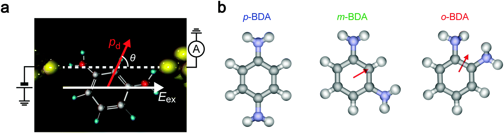
We herein report a systematic investigation of tunnelling transport through individual molecules in a solvent using sub-nanometer-spaced nanoelectrodes with calibrated separation (Fig. 1a). Benzenediamine (BDA) isomers having NH2 anchors at ortho (o-BDA), meta (m-BDA), and para (p-BDA) positions were employed mimicking amine-based aromatic ring moieties in biologically important macromolecules such as proteins and polynucleotides. These molecules were diluted in ultra-pure water or 1,2,4-trichrolobenzene (TCB) at 1 μM to verify the dipole effects. Single-molecule detection measurements were performed by tracing temporal changes in the current flow through the electrode gap in the solution at room temperature.
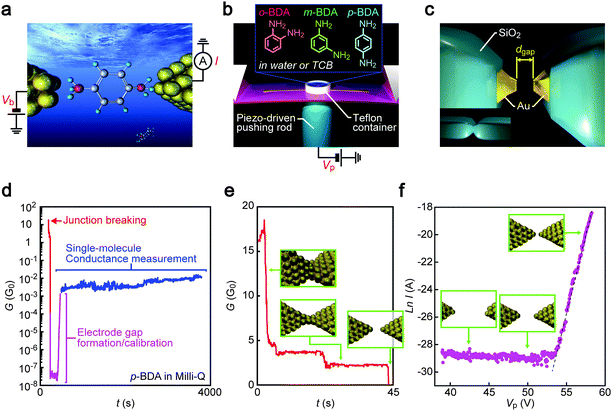 |
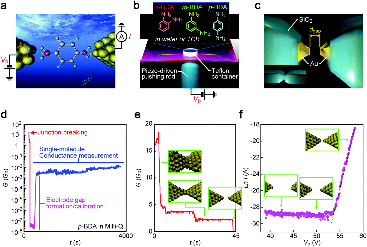
| | Fig. 1 Single-molecule conductance measurement procedure. (a) A schematic model of a single benzenediamine (BDA) molecule bridging between two Au electrodes. Current I through the junction was measured under the applied dc voltage Vb. (b) An illustration depicting the MCBJ set-up. Three BDA isomers were used as target molecules. The substrate bending was controlled through the voltage Vp for manipulations of the piezoactuator. (c) Insulator-protected Au nanoelectrodes with separation dgap formed by mechanically breaking the SiO2/Au junctions. (d–f) The course of electrode nanogap formation processes that consists of initial contact breaking (e), dgap–Vp calibration through linear fitting at the tunnelling current regime recorded during gap closure to I > 10−8 A as shown by a broken line (f), and single-molecule conductance measurements (d). | |
Experimental
Chemicals and materials
o-BDA, m-BDA, p-BDA, and TCB were used as received from Sigma-Aldrich Co. N,N-dimethylformamide was purchased from Wako Co. Ultra-pure water having a resistivity of 18.2 MΩcm was obtained through a Milli-Q Millipore system (Millipore Co.). Au and Cr sputtering targets were obtained from Sanyu Electron Co. AZ5206E and ZEP520A were purchased from Zeon Co. ZEP520A was diluted with ZEP-N to lower the viscosity and to have thin resist layers preferable for fine electron beam delineation.
Fabrications of insulator-protected MCBJs
Insulator-protected mechanically-controlled break junctions (MCBJs)19 were used to form two Au nanoprobes (Fig. 1b). The device consisted of a SiO2-coated freestanding Au junction lithographed on a polyimide layer of a phosphor bending beam (Fig. S1, ESI†). The following processes were used to fabricate the MCBJ chips. A 4 μm thick polyimide layer was coated on a phosphor bronze substrate by spin coating imide molecules followed by polymerization through baking at 200 degrees Celsius. A 40 nm thick SiO2 layer was then deposited on the polyimide layer by chemical vapour deposition (CVD). After that, microelectrodes were formed by photolithography using the AZ5206E resist, radio-frequency magnetron sputtering for the deposition of 40 nm thick Au with a 5 nm Cr adhesion layer, and a lift-off in N,N-dimethylformamide. Subsequently, nanojunctions were delineated by electron-beam lithography using the ZEP520A-7 resist. For this, a part of the microelectrodes was used as an external marker to overlay the nano-pattern in the 100 μm square area surrounded by three pairs of Au leads. After development, 100 nm thick Au was deposited by the magnetron sputtering process with a 2 nm Cr adhesive layer. Following the metal coating, the resist was lifted off by sonication in DMF. The thus obtained Au nanojunctions were exposed to a two-step reactive ion etching. In the first stage, CF4 etchant gas was used to remove the SiO2 layer uncovered by the Au pattern. Another dry etching was then implemented in O2 plasma to etch out the polyimide underneath the Au nanowires so as to free them from the substrate for the break junction experiments. Finally, the top surface was coated with a 40 nm thick SiO2 layer by the CVD process. Here, the free-standing length of Au nanobridges was designed to be 2 μm long. This, along with the phosphor bronze beam with a thickness of 0.5 mm and a distance of 12 mm between the two counter supports, yields the low attenuation factor20 of 3 × 10⁻⁵ essential for the fabrication of stable nanoelectrode systems viable for the single-molecule detections by tunnelling current measurements.10
Electrode gap formation
In experiments, the junctions were immersed in a molecular solution by placing a droplet in a Teflon ring attached on the substrate. Then, MCBJ substrates were mounted in a three-point bending configuration and bent mechanically using a piezo-driven pushing rod while recording the junction conductance G under the applied voltage Vb of 0.1 V using a picoammeter/source unit (Keithley 6487). By feedback-controlling the resulting deflection through the piezo-voltage with respect to G, Au nanocontacts were stretched slowly to induce self-breaking.21,22 This fine manipulation of contact mechanics allows the reproducible formation of sub-nanometer electrode gaps.22,23 Furthermore, the insulator-covered junction architecture served to confine the Au electrode area exposed to the solution for the tunnelling detection to the nanoscale fracture surface (Fig. 1c) that enabled suppression of the ionic contributions to the net current measured.19
Gap distance calibration
Adjustment of the electrode gap size dgap was implemented after the spontaneous Au contact breakdown. Specifically, dgap was first widened to above 1 nm by controlling the piezo-voltage Vp, which expands the actuator at 1 μm V−1, and subsequently narrowed gradually until the current through the Au electrodes I exceeded 10 nA. The thus obtained I–Vp plots revealed an exponential increase of the tunnelling current with a linear increase in log![[thin space (1/6-em)]](https://www.rsc.org/images/entities/char_2009.gif) I, indicating changes in dgap at a rate of rVp = 30 pm V−1. After the calibration, the gap was extended to a predefined distance ranging from 0.2 nm to 1.0 nm and the temporal change in I was recorded for more than 1000 seconds under the dgap conditions in the molecular solution at room temperature. The number of MCBJ chips utilized for the single-molecule conductance measurements was 24 in total. There were no notable differences in their device characteristics as confirmed by the dgap calibrations. The number of conductance traces recorded per BDA isomer was 41 (TCB) and 31 (water) for p-BDA, 45 (TCB) and 47 (water) for m-BDA, and 32 (TCB) and 27 (water) for o-BDA. Although these numbers are much smaller than that in typical break junction experiments where more than 1000 times of junction formation/breaking are examined by swiftly moving the electrodes into and out of contact,24 the present conditions compensate the number of trials by more than four orders of magnitude longer time period to record the conductance of molecular junctions in each measurement whereby obtaining abundant information concerning geometrical effects on the electron transport through the Au–BDA–Au structures.
I, indicating changes in dgap at a rate of rVp = 30 pm V−1. After the calibration, the gap was extended to a predefined distance ranging from 0.2 nm to 1.0 nm and the temporal change in I was recorded for more than 1000 seconds under the dgap conditions in the molecular solution at room temperature. The number of MCBJ chips utilized for the single-molecule conductance measurements was 24 in total. There were no notable differences in their device characteristics as confirmed by the dgap calibrations. The number of conductance traces recorded per BDA isomer was 41 (TCB) and 31 (water) for p-BDA, 45 (TCB) and 47 (water) for m-BDA, and 32 (TCB) and 27 (water) for o-BDA. Although these numbers are much smaller than that in typical break junction experiments where more than 1000 times of junction formation/breaking are examined by swiftly moving the electrodes into and out of contact,24 the present conditions compensate the number of trials by more than four orders of magnitude longer time period to record the conductance of molecular junctions in each measurement whereby obtaining abundant information concerning geometrical effects on the electron transport through the Au–BDA–Au structures.
First-principles calculations
Gaussian 09 package25 was employed to deduce the Au–BDA–Au junction configurations. The atomistic structures of a single-molecule junction were modelled by respectively placing an o-, m-, or p-BDA between two Au14 clusters through Au–NH2 links. Here, these two Au clusters are regarded as tips of electrodes. The geometry optimization and vibrational analysis were conducted by using the density functional theory (DFT) method with B3LYP hybrid functional. The basis sets were 6-31G+(d,p) for C, H, and N, and LANL2DZ for Au. In these calculations, we used the polarizable continuum model (PCM), by which the junctions within the dielectric continuum of water and TCB were respectively computed, to describe the solvent utilized in our single-molecule conductance measurements. The results were applied to estimate the dipole moments in BDAs.
Results and discussions
Single-molecule junction formations
Mechanical stretching of Au nanocontacts in molecular solution resulted in a step-wise decrease in the conductance G reflecting discrete contact deformation processes that involve atom rearrangements at the narrowest constriction upon reaching elastic limits under unidirectional straining (Fig. 1d and e).26 Right before the breakdown, plateaus were often observed near 1 G0 (G0 = 2e2/h is the conductance quantum, where e and h are the electron charge and Planck's constant, respectively) in conductance versus time (t) traces suggesting the formation of Au single-atom chains (Fig. 1e).27 At this stage, we ceased the mechanical control and let the atom-sized contacts to rapture spontaneously.21 After the breaking, calibration measurements were performed wherein the electrode gaps were closed slowly until the current I reached above 10 nA. Assuming dgap = 0 nm when I0 = 1 G0 × Vb = 7.5 μA, the gap distance at I = 10 nA was estimated through I = I0exp(−κdgap), where κ is the tunnelling decay constant deduced by a least-squares fitting to the lnI–Vp plots in linear regimes. The dgap value was then adjusted to a preset size ranging from 0.2 nm to 1 nm by posing additional strain according to the displacement ratio rVp through a piezo-control that opens the gap at a slow speed of 5 pm s−1. Though depending on the gap size conditions, the G–t curves acquired with the closely separated Au electrodes of the electrically-defined dgap revealed that the conductance sustained at around 10 mG0 over a prolonged time period. As the current through a tunnelling gap is expected to be lower than 0.1 nA (which corresponds to G < 0.01 mG0) under the dgap conditions measured, the elevated conductance states are naturally ascribed to charge transport through one or a few BDA molecules bridging between the Au nanoelectrodes.28
Conductance traces of BDA isomers
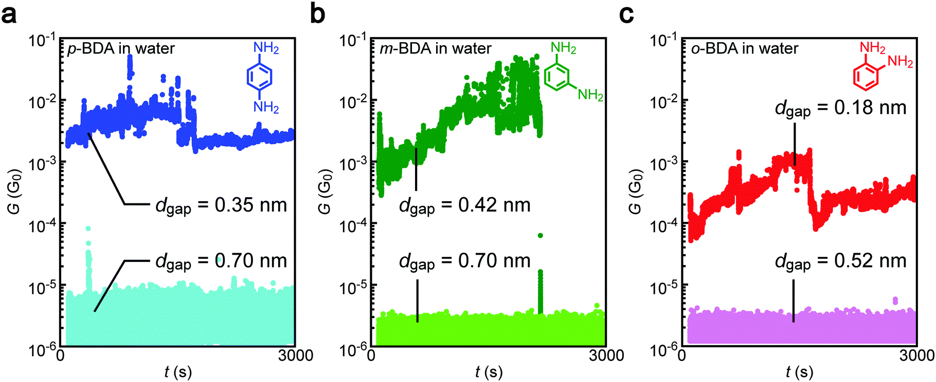
The conductance measurements identified the high-G characteristics indicative of the formation of Au–BDA–Au junctions in water as well as in TCB for all of the three isomers tested (Fig. 2). The conductance showed an order of magnitude fluctuation reflecting temporal changes in the Au–amine contact configurations and BDA conformations due to thermal perturbation at room temperature in liquids that give rise to 1/f-like noise.29,30 In some cases, the molecular contact was dissociated during the measurements as observed as a sudden decrease of G to below 10−6 G0. Meanwhile, the molecular features tended to disappear when the gap was extended to a certain extent whereas the actual conductance became lower than the detection limit of the current sensing system used.
 |
| | Fig. 2 Conductance traces after the electrode gap formation. (a–c) Conductance (G) versus time (t) curves recorded in aqueous solution of para- (p-BDA) (a), meta- (m-BDA) (b), and ortho-benzenediamine (o-BDA) (c). High-G states were observed when using narrow electrode gaps. | |
Electrode gap size dependence of single-molecule conductance
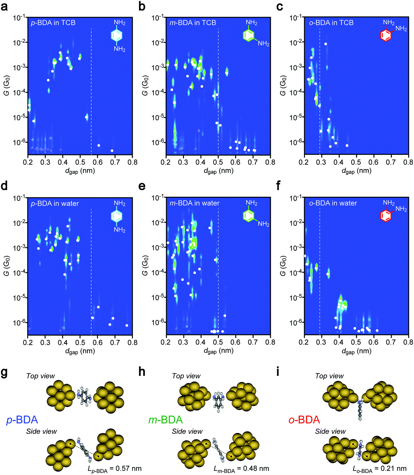
In efforts to shed some light on molecular signatures in the conductance traces, together with a motivation to evaluate the possible influence of the electric field on the conformations of current-carrying molecules, two-dimensional histograms of G and dgap were prepared. Each cluster of data at a constant dgap represents the scattering in G around the average value, shown as solid circles. The plots clearly display the aforementioned high conductance states of the p-BDA junctions around 10 to 0.1 mG0 at dgap < 0.5 nm, whereas the conductance tends to decrease suddenly to below the detection limit of our current sensing system at >0.6 nm. A similar electrode gap size dependence was observed for m- and o-BDAs. Here, it is noticed that the dgap onsets for the G drops are in good quantitative accordance with the interelectrode distance dBDA of Au–BDA–Au systems defined as the distance between the nearest Au atoms of the two facing clusters in the energy-optimized geometries deduced theoretically: Lp-BDA = 0.57 nm, Lm-BDA = 0.48 nm, and Lo-BDA = 0.21 nm (Fig. 3g–i; see also Tables S1 and S2, ESI†). This characteristic feature can be interpreted as reflecting the formation of molecular interconnects between the electrodes via Au–NH2 links when dgap < LBDA, and adversely the existence of a wide tunnelling space at the Au–BDA interface under dgap > LBDA where G decreases exponentially with the through-space bond length,30 which in turn suggests the feasibility of the diamine molecules as a chemically designed infinitesimal ruler to scale the electrode gaps at a sub-nanometer resolution.31 The present results also serve to verify the high mechanical stability of the nanoelectrode system to form and hold the closely spaced metal probes in liquid for over hundreds of seconds accompanied by good controllability of the spacing with accuracy higher than 0.1 nm (as judged by the fact that no sign of molecular bridging can be found in Fig. 3 at dgap > LBDA + 0.1 nm). Meanwhile, low-G states below 10−5 G0 were also detected occasionally even when dgap < LBDA (displayed as grey circles in Fig. 3) reflecting the stochastic nature of molecular trapping,11,12 wherein Brownian motions in the solvent fail in some cases to let molecules to move into the inter-electrode space within the time period of the tunnelling current measurements.
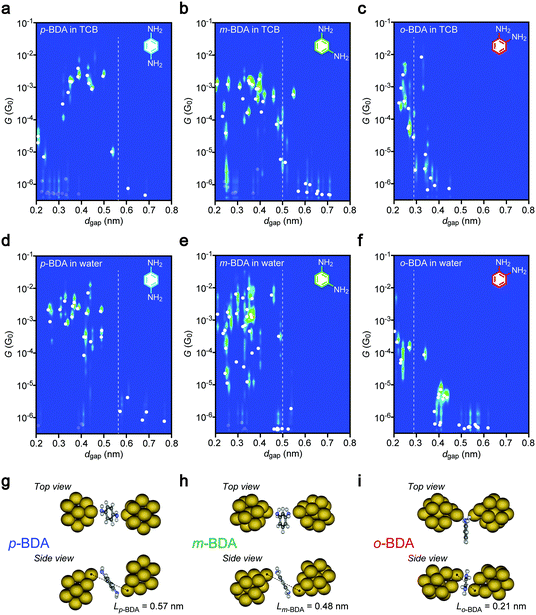 |
| | Fig. 3 Electrode gap size dependence of molecular junction conductance. (a–c) G-dgap two-dimensional histograms constructed with the conductance traces recorded for p-BDA (a), m-BDA (b), and o-BDA (c) in 1,2,4-trichrolobenzene (TCB). Broken lines denote the molecular length LBDA of BDAs measured. White plots are the average conductance at each dgap condition, which are made transparent for those showing low values<10−5 G0 at dgap < LBDA for the sake of clarity. (d–f) The same series of data acquired for the three BDA isomers in water. (g–i) Energy-optimized molecular junction structures. Dashed lines depict the distance between the anchor Au atoms. | |
Molecular junction conductance of BDA isomers
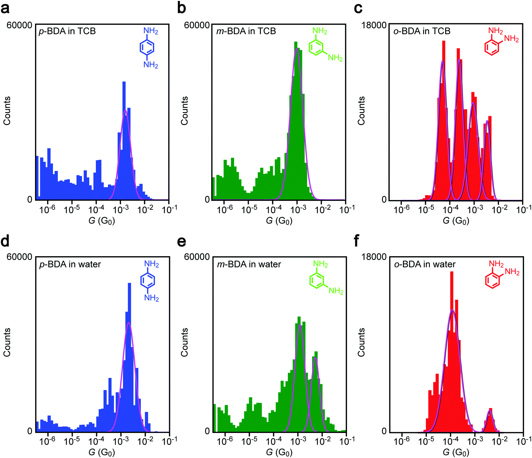
Having confirmed the dgap conditions to bridge BDAs to Au nanoelectrodes, we evaluated the anchor-position dependence on the single-molecule conductance. Fig. 4a–c show conductance histograms constructed using the I–t data obtained in TCB with sub-molecular-sized electrode gaps. It reveals a pronounced peak for p-BDA at 1.6 mG0. The narrow distribution in G is attributed to the limited number of adsorption sites of amines on the Au surface via coordination bonding that effectively suppresses the variation in formable junction configurations, thereby enabling observations of a well-defined single-molecule conductance state.28,32 Although the distribution extends to cover the typical value of G = 6 mG0 reported in previous literature, p-BDAs prefer to take lower G states under the present conditions, the discrepancy of which is presumably due to the difference in the break junction procedures employed:33 while conventional techniques create metal–molecule–metal structures during the mechanical rupture of molecule-adhered metal contacts, the present method does the opposite whereas nanoelectrodes are manipulated to move closer with each other to the predefined distance and wait for a chance to capture BDAs in the gap, in sense of single-molecule fishing34 in the solvent using the metal probes as a hook, whereas enough time is given for the relaxation of the junction geometries to an energetically favourable configuration.
 |
| | Fig. 4 Solvent effects on conductance variations in Au–BDA–Au junctions. (a–c) G-histograms constructed using conductance data obtained using sub-molecular-sized electrode gaps for p- (a), m- (b), and o-BDA (c) in TCB. (d–f) The conductance distributions of the BDA isomers in water. Solid curves are Gaussian fits to the peak features. | |
Similar to p-BDA, m-BDA also showed a sharp feature in the G distribution signifying the geometry-insensitive transmission characteristics of Au–amine anchored molecular junctions, but with a slight shift to around 1.0 mG0. The lower conductance agrees qualitatively with the first-principles calculations of the electronic structures of m-BDAs that predict larger energy difference between the current carrying orbital35 and the electrode Fermi level EF (=−5.1 eV assumed from the experimental work function36,37) compared to the p-BDA counterpart (Table 1), which is in accordance with the previous literature.38
Table 1 Electronic properties of Au–BDA–Au junctions
| Molecules |
Solvent |
Conductance (G0) |
HOMO−4 (eV) |
Dipole moment (D) |
|
o-BDA |
Water |
2.0 × 10⁻³ |
−5.17 |
1.83 |

|
| TCB |
3.5 × 10⁻³, 0.3 × 10⁻³ |
−5.39 |
1.55 |
| 0.9 × 10⁻³, 0.05 × 10⁻³ |
|
m-BDA |
Water |
6.1 × 10⁻³, 1.1 × 10⁻³ |
−5.25 |
1.56 |

|
| TCB |
1.0 × 10⁻³ |
−5.45 |
1.36 |
|
p-BDA |
Water |
2.0 × 10⁻³ |
−5.19 |
0 |

|
|
|
TCB |
1.6 × 10⁻³ |
−5.37 |
0 |
Besides the Fermi alignment, previous studies suggest a possible effect of quantum interference on the coherent electron tunnelling in the BDA junctions. While no such phenomenon is expected to occur in p- and o-BDA, as judged from the molecular structures, the atom-counting model39,40 predicts the presence of an isolated site in the benzene ring for m-BDA. The resulting destructive quantum interference has been demonstrated both theoretically39,40 and experimentally41 to prohibit charge transport via π electrons whereby rendering low conductance states through the remaining σ bond tunneling.42–44 However, we notice that the molecular conductance of m-BDA in the present work is relatively high and not so different from that of p-BDA. Therefore, we speculate that the interference-induced transmission node locates at an energy far from the Fermi level, and hence engenders only small influence on the single-molecule conductance.45
In addition to the representative conductance states, it is noticeable that there are features at G < 10−4 G0 in Fig. 3(a, b) and (d, e). The low-G counts stem from the conductance data after spontaneous Au–amine bond dissociation during the measurements (Fig. 2b).
On the other hand, we found up to four G peaks for o-BDA. These distinct conductance states are confirmed to be present in the separate histograms (Fig. S2, ESI†). Furthermore, the tunnelling conductance in an open gap is anticipated to be lower than 10−5 G0 at dgap > 0.18 nm (tentatively estimated with a vacuum barrier height of 5.1 eV for Au). It is therefore likely that there are equally stable multiple choices of configurations for the ortho-isomer with adjacently positioned anchor groups to bridge across the sub-molecular-sized Au nanogap in the organic solvent (for instance, a through-space bond motif having two amines coordinated to one side of the electrodes38 in addition to the configuration derived by DFT calculations (Fig. 3i)). We leave the assignment of junction geometries to the characteristic conductance states observed here as future works, which may call for molecular dynamics simulations of o-BDAs in nanoelectrode systems.
Solvent dependence of BDA conductance
Comparing G histograms of p-BDAs in TCB and water, we find no notable difference except a sub-mG0 increment in the single peak position that would be attributed to a change in the electrode work function by the adsorption of solvent molecules at the undercoordinated Au sites.46–48 In sharp contrast, a drastic change in the conductance was detected for the other BDAs: a new peak appeared at 6.1 mG0 in water in addition to the original 1 mG0 feature in TCB for m-BDA; more strikingly, one specific G-state was virtually singled out in aqueous media from the multiple conductance states of o-BDA observed in the organic liquid. Unlike the solvent effects on the tunnelling barrier height,46Fig. 4 demonstrates appearance/dis-appearance of the junction conductance states that may imply an intriguing impact of solvent properties on the choice of Au–BDA–Au configurations achievable under the conditions tested.
Dipole effects on single-molecule conductance
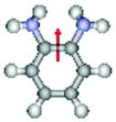
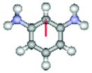
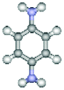
We now explore the roles of electric field on the molecular conformations and concomitant effects on the junction conductance. It is naturally supposed that polar molecules experience coulombic interaction in a dc-biased electrode gap (Fig. 5).9,49,50 Particularly, having equal amounts of positive and negative charges, the electrostatic force acting on a molecule in a uniform electric field Eex is essentially zero. Nevertheless, when there is a misaligned dipole by angle θ with respect to the field direction, the external field yields a torque N = pdEexsinθ, where pd is the dipole moment (Fig. 5a). Hence, the dipole–electric field interactions would affect the molecular conformations to direct along Eex when the gain of potential energy U = pdEexcosθ is equivalent or larger than the thermal energy kBT. To examine the contributions of electrostatic effects on the variations in G, we estimated dipole moments for the BDA isomers in TCB and water. Consideration of the resonance structures predicts positive charges on NH2. As summarized in Table 1, however, the p-BDA has zero net moment, evident from the Ci symmetry of the diamine architecture that completely cancels the intramolecular dipoles (Fig. 5b). The absence of dipole moments is consistent with the small solvent effects seen in the variations in G for the para-isomer (Fig. 4a and d). By contrast, pd increases to 1.36 and 1.55 D for m- and o-PDA in TCB, respectively, reflecting the degrees of broken symmetry in the C2 symmetric molecules. A rough estimation of the strength of dipole interactions with these pd values gives U = 16 meV for o-BDA, assuming that the molecules form an angle of 0° with the electric field under the huge electrical field of Vb/dgap = 5 MV cm−1 with dgap = 0.20 nm, which is of the same order as kBT = 25 meV at 293 K, and hence predicts a non-negligible influence of Eex on the molecular junction configurations for the ortho-molecules. Furthermore, theoretical modelling pointed out a 17% increase in pd of o-BDAs by changing the media to water whereby augmenting the field-effect to 19 meV (Table 1). This can be understood within a framework of the Onsager reaction field model51 as a result of induced polarization via mutual interaction between dipoles of surrounding H2O molecules and benzenediamines. Although the difference is not so large, it qualitatively explains the marked change in the conductance variations observed in Fig. 4: the coulombic forces exerted on o-BDA in water are strong enough to align the dipole moment along the electric field by causing a change in the conformations to a specific orientation,49,50 thereby filtering the accessible conductance states to a single one (Fig. 4c and f). Whereas the dipole effect would be effective to regulate the junction configurations for the ortho-isomer, where one side of the electrodes are bonded through-space via less overlap of molecular orbitals to Au local density of states, that of sub-eV electrostatic energy seems to be too small to drastically affect the structure of m-BDAs rigidly bonded via Au–NH2 linkages with a bonding strength of 0.7–0.8 eV,52,53 as demonstrated by the slight modifications in G-variations by changing the solvent from TCB to water (Fig. 4b and e). These results elucidate the impact of the electric field on the molecular junction configurations whose significance on the single-molecule conductance increases when electrode–molecule links are weak compared to the torque produced on the molecular dipoles.
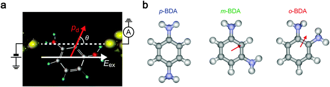 |
| | Fig. 5 Dipole–electric field interactions. (a) Coulombic interaction between a molecular dipole and external electric field in an electrode gap. θ defines the angle between the directions of the field and the dipole moment. (b) Dipole moments in BDAs. Arrows point from negative to positive potentials. Note that p-BDA has no net dipole moment due to the symmetric position of the amines. | |
Conclusions
We studied dipole effects on single-molecule tunnelling junction conductance in a liquid. Lithographed MCBJs were employed to create a pair of electrodes with sub-nanometer separation. The gap size was calibrated through examination of the tunnelling current decay with respect to the piezo-controlled electrode displacements. A crossover from single-molecule electron transport to space tunnelling was found at a gap distance around the molecular length, which indicates the potential use of single-molecules as a ruler to measure the nanoscale distance between two electrodes. Conductance variations of ortho-benzenediamines become smaller in water compared to that in 1,2,4-trichrolobenzene by virtue of the field alignment of the molecular dipole moment in the electrode gap that restricts the available junction configurations formed in the experiments. In contrast, having a zero net dipole moment due to the self-cancelled local charges within the symmetric diamine architecture, the para-isomer showed little difference in the conductance upon changing the solvent. This finding offers a novel concept for achieving better sensing capability of single-biomolecules by tunnelling current measurements.
Acknowledgements
A part of this work was supported by the Japan Society for the Promotion of Science (JSPS) KAKENHI Grant Number 15H03543, the Program for Creating Future Wisdom (Osaka University, selected in 2014), and “Nanotechnology Platform Project (Nanotechnology Open Facilities in Osaka University)” of the Ministry of Education, Culture, Sports, Science and Technology, Japan [No. F-12-OS-0016]. M. Tsutsui acknowledges support from the Asahi Glass Foundation and Kansai Research Foundation for technology promotion.
Notes and references
- U. E. Metzger, Chem. Rev., 2015, 115, 5056–5115 CrossRef PubMed.
- L. Sun, Y. A. Diaz-Fernandez, T. A. Gschneidtner, F. Westerlund, S. Lara-Avila and K. Moth-Poulsen, Chem. Soc. Rev., 2014, 43, 7378–7411 RSC.
- S. Aradhya and L. Venkataraman, Nat. Nanotechnol., 2013, 8, 399–410 CrossRef CAS PubMed.
- N. A. Zimbovskaya and M. R. Pederson, Phys. Rep., 2011, 509, 1–87 CrossRef CAS.
- M. Di Ventra and M. Taniguchi, Nat. Nanotechnol., 2016, 11, 949–953 CrossRef PubMed.
- S. Lindsay, Nat. Nanotechnol., 2016, 11, 109–111 CrossRef CAS PubMed.
- D. Xiang, X. Wang, C. Jia, C. T. Lee and X. Guo, Chem. Rev., 2016, 116, 4318–4440 CrossRef CAS PubMed.
- Y. Wang, Q. Wang and Z. Wang, Front. Genet., 2015, 5, 449 Search PubMed.
- J. Lagerqvist, M. Zwolak and M. Di Ventra, Nano Lett., 2006, 6, 779–782 CrossRef CAS PubMed.
- M. Tsutsui, M. Taniguchi, K. Yokota and T. Kawai, Nat. Nanotechnol., 2010, 5, 286–290 CrossRef CAS PubMed.
- S. Huang, J. He, S. Chang, P. Zhang, F. Liang, S. Li, M. Tuchband, A. Fuhrmann and S. Lindsay, Nat. Nanotechnol., 2010, 5, 868–873 CrossRef CAS PubMed.
- M. Tsutsui, S. Rahong, Y. Iizumi, T. Okazaki, M. Taniguchi and T. Kawai, Sci. Rep., 2011, 1, 46 Search PubMed.
- M. Zwolak and M. Di Ventra, Nano Lett., 2005, 5, 421–424 CrossRef CAS PubMed.
- P. Pang, B. A. Ashcroft, W. Song, P. Zhang, S. Biswas, Q. Qing, J. Yang, R. Nemanich, J. Bai, J. T. Smith, K. Reuter, V. S. K. Balagurusamy, Y. Astier, G. Stolovitzky and S. Lindsay, ACS Nano, 2014, 8, 11994–12003 CrossRef CAS PubMed.
- N. Sergueev, L. Tsetseris, K. Varga and S. Pantelides, Phys. Rev. B: Condens. Matter Mater. Phys., 2010, 82, 073106 CrossRef.
- H. Wang and Y. Leng, J. Phys. Chem. C, 2015, 119, 15216–15223 CAS.
- W. R. French, C. R. Lacovella and P. T. Cummings, ACS Nano, 2012, 6, 2779–2789 CrossRef CAS PubMed.
- M. Krems, M. Zwolak, Y. V. Pershin and M. Di Ventra, Biophys. J., 2009, 97, 1990–1996 CrossRef CAS PubMed.
- A. Arima, M. Tsutsui, T. Morikawa, K. Yokota and M. Taniguchi, J. Appl. Phys., 2014, 115, 114310 CrossRef.
- N. Agraït, A. L. Yeyati and J. M. van Ruitenbeek, Phys. Rep., 2003, 377, 81 CrossRef.
- M. Tsutsui, K. Shoji, M. Taniguchi and T. Kawai, Nano Lett., 2008, 8, 345 CrossRef CAS PubMed.
- K. O'Neill, E. A. Osorio and H. S. van der Zant, Appl. Phys. Lett., 2007, 90, 133109 CrossRef.
- M. Tsutsui, M. Taniguchi and T. Kawai, Appl. Phys. Lett., 2008, 93, 163115 CrossRef.
- B. Xu and N. J. Tao, Science, 2003, 301, 1221–1223 CrossRef CAS PubMed.
-
M. J. Frisch, et al., Gaussian 09, Revision C.01, Gaussian, Inc, Wallingford CT, 2009 Search PubMed.
- G. Rubio, N. Agrait and S. Vie ira, Phys. Rev. Lett., 1996, 76, 2302–2305 CrossRef CAS PubMed.
- H. Ohnishi, Y. Kondo and K. Takayanagi, Nature, 1998, 395, 780 CrossRef CAS.
- L. Venkataraman, J. E. Klare, I. W. Tam, C. Nuckolls, M. S. Hybertsen and M. L. Steigerwald, Nano Lett., 2006, 6, 458–462 CrossRef CAS PubMed.
- D. Xiang, T. Lee, Y. Kim, T. Mei and Q. Wang, Nanoscale, 2014, 6, 13396–13401 RSC.
- O. Adak, E. Rosenthal, J. Meisner, E. F. Andrade, A. N. Pasupathy, C. Nuckolls, M. S. Hybertsen and L. Venkataraman, Nano Lett., 2015, 15, 4143–4149 CrossRef CAS PubMed.
- N. Prokopuk and K.-A. Son, J. Phys.: Condens. Matter, 2008, 20, 374116 CrossRef PubMed.
- S. Y. Quek, L. Venkataraman, H. J. Choi, S. G. Louie, M. S. Hybertsen and J. B. Neaton, Nano Lett., 2007, 7, 3477–3482 CrossRef CAS PubMed.
- Z. Li and D. S. Kosov, Phys. Rev. B: Condens. Matter Mater. Phys., 2007, 76, 035415 CrossRef.
- Z. Liu, S.-Y. Ding, Z.-B. Chen, X. Wang, J.-H. Tian, J. R. Anema, X.-S. Zhou, D.-Y. Wu, B.-W. Mao, X. Xu, B. Ren and Z.-Q. Tian, Nat. Commun., 2011, 2, 305 CrossRef PubMed.
- Our calculations found HOMO−4 as a delocalized molecular orbital that contributed most to the charge transmission.
- O. Olubosede, O. M. Afolabi, R. S. Fayose, E. O. Oniya and A. C. Tomiwa, Appl. Phys. Res., 2010, 3, 171–178 Search PubMed.
- H. B. Michaelson, J. Appl. Phys., 1977, 48, 4729–4733 CrossRef CAS.
- M. Kiguchi, H. Nakamura, Y. Takahashi, T. Takahashi and T. Ohto, J. Phys. Lett., 2010, 114, 22254–22261 CAS.
- K. Yoshizawa, T. Tada and A. Staykov, J. Am. Chem. Soc., 2008, 130, 9406–9413 CrossRef CAS PubMed.
- T. Markussen, R. Stadler and K. S. Thygesen, Nano Lett., 2010, 10, 4260–4265 CrossRef CAS PubMed.
- M. Taniguchi, M. Tsutsui, R. Mogi, T. Sugawara, Y. Tsuji, K. Yoshizawa and T. Kawai, J. Am. Chem. Soc., 2011, 133, 11426–11429 CrossRef CAS PubMed.
- D. Cardmone, C. A. Stafford and S. Mazumdar, Nano Lett., 2006, 6, 2422–2426 CrossRef PubMed.
- S. –H. Ke and W. Yang, Nano Lett., 2008, 8, 3257–3261 CrossRef PubMed.
- G. C. Solomon, D. Q. Andrews, T. Hansen, R. H. Goldsmith, M. R. Wasielewski, R. P. van Duyne and M. A. Ratner, J. Chem. Phys., 2008, 129, 054701 CrossRef PubMed.
- J. Xia, B. Capozzi, S. Wei, M. Strange, A. Batra, J. R. Moreno, R. J. Amir, E. Amir, G. C. Solomon, L. Venkataraman and L. M. Campos, Nano Lett., 2014, 14, 2941–2945 CrossRef CAS PubMed.
- V. Fatemi, M. Kamenetska, J. B. Neaton and L. Venkataraman, Nano
Lett., 2011, 11, 1988–1992 CrossRef CAS PubMed.
- B. Capozzi, J. Xia, O. Adak, E. J. Dell, Z.-F. Liu, J. C. Taylor, J. B. Neaton, L. M. Campos and L. Venkataraman, Nat. Nanotechnol., 2015, 10, 522–527 CrossRef CAS PubMed.
- D. C. Milian, O. A. Al-Owaedi, M.-C. Oerthel, S. Marques-Gonzalez, R. J. Brooke, M. R. Bryce, P. Cea, J. Ferrer, S. J. Higgins, C. J. Lambert, P. J. Low, D. Z. Manrique, S. Martin, R. J. Nichols, W. Schwarzacher and V. M. Garcia-Suarez, J. Phys. Chem. C, 2011, 11, 1988–1992 Search PubMed.
- A. W. Ghosh, T. Rakshit and S. Datta, Nano Lett., 2004, 4, 565–568 CrossRef CAS.
- V. Meded, A. Bagrets, A. Arnold and F. Evers, Small, 2009, 5, 2218–2223 CrossRef CAS PubMed.
- L. Onsager, J. Am. Chem. Soc., 1936, 58, 1486–1493 CrossRef CAS.
- M. Tsutsui, M. Taniguchi and T. Kawai, J. Am. Chem. Soc., 2009, 131, 10552–10556 CrossRef CAS PubMed.
- M. Kamenetska, M. Koentopp, A. C. Whalley, Y. S. Park, M. L. Steigerwald, C. Nuckolls, M. S. Hybertsen and L. Venkataraman, Phys. Rev. Lett., 2009, 102, 126803 CrossRef CAS PubMed.
Footnote |
| † Electronic supplementary information (ESI) available. See DOI: 10.1039/c6nh00088f |
|
| This journal is © The Royal Society of Chemistry 2016 |
Click here to see how this site uses Cookies. View our privacy policy here. 
 Open Access Article
 This Open Access Article is licensed under a Creative Commons Attribution-Non Commercial 3.0 Unported Licence