
 Open Access Article
 This Open Access Article is licensed under a
 Creative Commons Attribution 3.0 Unported Licence
Conjugated polyelectrolyte nano field emission adlayers†
M. T.
Cole‡
*a,
R. J.
Parmee‡
a,
A.
Kumar‡
a,
C. M.
Collins
a,
M. H.
Kang
a,
J.
Xiao
a,
C.
Cepek
 b,
X.
Yuan
c and
W. I.
Milne
ad
b,
X.
Yuan
c and
W. I.
Milne
ad
aDepartment of Engineering, Electrical Engineering Division, Cambridge University, CB3 0FA, UK. E-mail: mtc35@cam.ac.uk
bIstituto Officina dei Materiali, CNR, Strada Statale 14, Trieste, Italy
cSchool of Physical Electronics, University of Electronic Science & Technology of China, Chengdu 610054, China
dCollege of Information Science and Electronic Engineering, Zhejiang University, Hangzhou, 310027, China
First published on 9th May 2016
Abstract
Here we report on a straightforward and rapid means of enhancing the field electron emission performance of nascent vertically aligned multi-walled carbon nanotubes by introducing a polar zwitterionic conjugated polyelectrolyte adlayer at the vacuum–emitter interface. We attribute the observed 66% decrease in turn-on electric field to the augmented emitter micro-morphology and shifted surface band structure. The composite emitters can be optically modulated by exploiting the absorption cross-section of the solution cast adlayer, which increases the local carrier concentration which broadens the effective electrostatic shape of the emitter during optical excitation. Assessment via scanning anode field emission microscopy reveals a 25% improvement in DC time stability, a significant reduction in long-term hysteresis shift, and a threefold increase in bandwidth during pulsed mode operation.
Conceptual insightsCarbon nanotubes, and the wider class of graphitic nanocarbons, have a proven potential as efficient field electron emission sources though the enhancement of their emission characteristics upon adlayer inclusion is little understood to date. Here we demonstrate a simple adlayer scheme capable of enhancing the native field emission properties of as-grown chemical vapour deposited carbon nanotubes through simultaneous geometric and electronic enhancement using a new class of nanotube–vacuum interface adlayer; anionic zwitterionic conjugated polyelectrolytes (ZCPEs). Adlayers preserve the beneficial geometries and high aspect ratios of these nanoscale one-dimensional structures whilst concurrently enhancing the emission performance. Though a wide set of adlayer materials have been considered elsewhere, of which almost all have exclusively focused on low work function metal over-coatings, here we report on the use of engineered polar conjugated polyelectrolyte adlayers. We find that our ZCPE adlayer mediates a fourfold decrease in free carrier concentration at the upper most emission surface which reduced the deleterious effects of nearest neighbour shielding common to highly-packed carbon nanotube based emitters. The dominant space charge limiting mechanism, and subsequent observed barrier transmission, was found to be consistent with Lampert–Rose, with potential specific deviation attributed to depopulation of local, optically active, trap states. The surface dipole, the magnitude of which relates intimately to the choice of side chain, effectively reduces the emitter–vacuum barrier increasing the transmission efficiency at lower electric fields. Whereas cationic ZCPEs, such as those with nitrogen side groups, will likely increase the turn-on field our evidence suggests that anionic polymers favour reduced turn-on fields, with our results highlighting a clear strategy for the use of engineered polar molecules, coupled to the wider family of novel nanocarbon allotropes, as a means to realise inexpensive and readily adopted high current density electron sources for use in high resolution microscopy and advanced metrology, next generation free electron lasers, desktop scale particle accelerators, along with high bandwidth travelling wave tubes and pulsed X-ray sources. |
Introduction
Electron emission technologies are ubiquitous; from X-ray sources1 and electron microscopes,2 to travelling wave tubes,3 microwave amplifiers,4 high dynamic range displays,5,6 and free electron lasers.7 Nevertheless, many such applications employ electron emitters based on arrays of conventionally micro-fabricated Spindt-like, refractory metal tips. However, the recent emergence of controlled bottom-up synthesis of various one- and two-dimensional nanomaterials brings to the fore the potential for new emitter morphologies with enhanced functionalities, coupled with cheap and highly parallelised fabrication en masse. In this respect, carbon nanotubes (CNTs), and the many graphitic variants thereof, have emerged as one such leading candidate class of materials for the realisation of advanced electron sources.8–10 Nevertheless, for technologically relevant high currents such devices must be operated at electric fields near their breakdown limits. This adversely affects their lifetime. Reduction in driving voltages is critical. The addition of various adlayers is one possible strategy towards achieving high current density emission with low turn-on fields. Various exotic adlayers have been considered to date.11–20 However, little has been reported on the use of conjugated polyelectrolytes (CPEs) which are strong contenders for electron emission applications due to their potential for efficient electron injection and unique transport characteristics.21 Here we report on the use of zwitterionic conjugated polyelectrolytes as a new class of field emission adlayer.Field emission is a surface sensitive process; the merits of adlayers on electron emission from carbon nanotubes have been highlighted elsewhere.21 In the past decade, conjugated polymers have become recognised as an important class of organic semiconductor that have yet to be widely employed to enhance field electron emission. Using degenerately doped silicon, Musa et al., coated a 5 μm thin film of conjugated polymer electrolyte, regioregular poly(3-octylthiophene) (P3OT), showing ultra-low threshold field of 0.2 V μm−1. At this time the work was not extended to the coating of nanostructures with beneficially high aspect ratios, nor were non-neutral polymer layers considered. In the present report we coat vertically aligned, high aspect ratio carbon nanotubes with a polar zwitterionic conjugated polyelectrolyte (ZCPE); the ZCPE has a conjugated polyfluorene backbone with sulfonate zwitterionic side chains on an alternative fluorene unit. ZCPEs are known interfacial modifiers in polymer light-emitting diodes22 and in organic photovoltaics.23 They have been used to improve the electron transfer process at various interfaces and when coupled to carbon nanotubes as existing high aspect ratio nano-scaffolds, they may prove to be an exciting platform for enhanced emission. Here we show the first detailed studies on the use of polar conjugated polymer electrolytes as adlayers to enhance the native field emission from carbon nanotubes.
Results & discussion
Multi-walled carbon nanotube synthesis was conducted on 10 × 10 mm degenerately n-doped 〈111〉 Si that was DC magnetron sputtered with a bilayer catalyst of 10 nm Al and 2 nm Fe. These catalyst samples were then loaded into a commercially available thermal chemical vapour deposition reactor (Black Magic, Aixtron Ltd) and heated to 700 °C (5 °C s−1) at 25 mbar under an atmosphere of 192 (±3) sccm NH3: 8 (±1) sccm C2H2 to initiate MWCNT growth. Following growth, the etched Si backside was diamond scribed to remove the thermal oxide and subsequently painted with a colloidal Ag paste, diluted in MIBK, to ensure good connectivity with the ground plate during the field emission measurements. The as-synthesised MWCNT forests had a typical packing density of 3.0 × 1010 cm−2 (Fig. 1(b)), with individual MWCNTs some 7.7 (±2.3) nm in diameter, 3.45 (±0.35) μm in length, formed from an average of 5 (±2) graphitic side walls (Fig. 1(c)). HR-TEM images were acquired using an FEI Philips Tecnai operated at 100 keV. Raman spectroscopy (515 nm) showed an 〈ID/IG〉 of 1.05 (±0.05). ZCPE, F(NSO3)2 synthesis is described in detail elsewhere.22 In brief; a standard Suzuki condensation polymerization of 2,7-bis(1,3,2-dioxaborolan-2-yl)-9,9-dioctylfluorene with 2,7-dibromo-9,9-bis((N,N-dimethylamino)ethanyl)fluorine, in the presence of Pd was used. The quaternisation of the neutral polymer, by 1,4-butane results in sulfobetaine zwitterionic F(NSO3)2. F(NSO3)2 was dissolved in methanol to prepare a 2 mg mL−1 solution. The as-prepared ZCPE was drop cast (ca. 10 mL) onto the MWCNT samples and allowed to dry at STP for 10 min. By stylus profilometry (Dektak IIA) the ZCPE adlayer was measured to be approximately 290 (±60) nm thick (when equivalently deposited on Si control samples), with the ZCPE crystallising primarily on the uppermost surface of the MWCNT forest. Electron microscopy revealed that the ZCPE adlayer is thinner in situ than this upper-bound estimate would suggest. Scanning electron micrographs were acquired using a Carl Zeiss Gemini and FEI Philips XL30 sFEG, both operated at 20 keV. Optical microscope images were acquired using a Nikon eclipse ME600L fitted with a ×50 aperture. Images were analysed using the DiameterJ ImageJ plugin.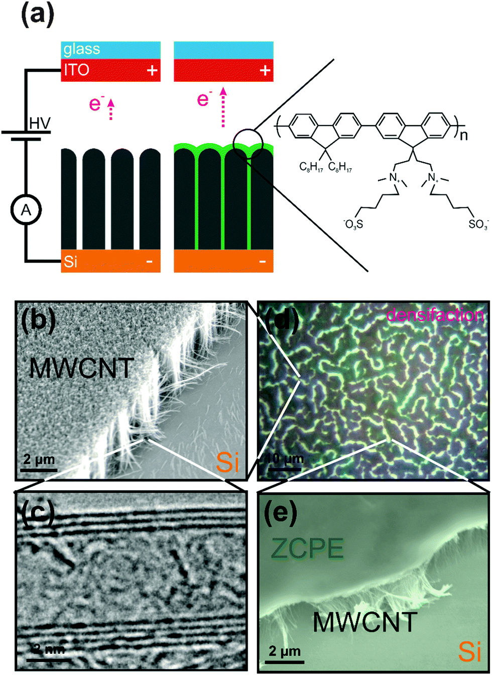 | ||
| Fig. 1 (a) Scheme illustrating the diode measurement set-up and the ZCPE coated MWCNT, alongside the F(NSO3)2 chemical form of the ZCPE. (b) A scanning electron micrograph of a typical, as-synthesised vertically aligned MWCNT sample (scale bar: 2 μm) and (c) high-resolution transmission electron micrograph of a single MWCNT (scale bar: 2 nm). (d) Optical micrograph of a densified MWCNT/ZCPE sample (scale bar: 10 μm), and a (e) scanning electron micrograph of a ZCPE coated MWCNT forest (scale bar: 2 μm). | ||
To mediate ZCPE deposition, a methanol solvent was used. The solvent augments the morphology of the nascent MWCNT forests, as shown in Fig. 1(d and e), resulting in the formation of a densified micro-morphology.24,25 Such methodology leads to zones of reduced areal packing density, in turn leading to reduced nearest neighbour electrostatic shielding, and a corresponding reduction in turn-on field (Eon, defined as the electric field required to stimulate the emission of 1 nA). ZCPE treatment densifies the nascent MWCNT forest by around 30%, increasing the local packing density in the densified regions to 4 × 1010 cm−2. We stress that the liquid phase densification did not reduce the degree of electrical interconnection within the forest; samples consistently showed effective macroscale porosities lower than that required to maintain a percolative network. Indeed, two-terminal stylus contact macroscale sheet resistance measurements showed similarly conductive thin films following the ZCPE treatment. Densification increased the edge density, manifestly increasing the number of electron emission sites. The adlayer results in the formation of vein-like gaps, with the intervening ZCPE mesas being of uniform height. The veins had a width of 1.9 (±0.6) μm with, on average, 4.6 × 10⁻² intersections per μm2. Orientation analysis of the veins showed that the liquid-phase densification did not result in any preferential alignment. The mean crack width, g, (absence of MWCNTs) was 1.13 (±0.43) μm, which we find is of a comparable magnitude to h, where h is the height of the MWCNTs (h = 3.45 (±0.35) μm).
To further probe the enhancement, in order to decouple the geometry from any surface adjustment, electrostatic simulations were conducted. Here we assumed a simplified Fowler–Nordheim like emission profile fitted to empirical data from fully covered nascent MWCNT I–E data. The measured current density per unit area adopt a general form, J = AE2![[thin space (1/6-em)]](https://www.rsc.org/images/entities/char_2009.gif) exp(−B/E), which upon fitting gave A = 1.12 × 10⁻⁸ A V−2, and B = 6.53 × 10⁷ V m−1 (R2 = 0.594). We stress such fitting values give a good fit in the specific turn-on bias window of interest. The experimental emission area was 0.39 cm2, and the measured beam current density is termed J0 in this full-coverage case. The effect of the MWCNT forest densification on the emission performance was simulated using CST©. To give a tractable computation time, a square emission area of 10 μm × 10 μm was adopted for all simulations, with current densities calculated thereon. To obtain Eon as a function of the variation in mark/space ratio, simulating the effects of the vein-like structures observed in experimentation, the emission area was divided into 16 sections, with each section simplified to a square emission site. Each emission site had sides of length g. The distance between emission sites was G. Eon was minimised when the crack: height ratio, ρ ∼ 3. For ρ > 3 we find a deleterious increase in Eon (and reduction in J), and for ρ < 3 Eon near-linearly decreases. In the present case, where ρ = 0.33, though we remain some way off the maximally reduced Eon, it does nevertheless remain improved relative to the nascent MWCNT forest (g = 0) case. Although the emission area is decreased in our various side length simulations, the emission current of each section is increased and the beam current density maintained. Indeed, when g = 0.7 μm and G = 2.4 μm; our models suggest an Eon = 1.52 V μm−1, consistent with our empirical findings from the densified samples. This highlights the critical role that the densification process, and more generally the need for optimised emission morphologies, plays on reducing the turn-on field.
exp(−B/E), which upon fitting gave A = 1.12 × 10⁻⁸ A V−2, and B = 6.53 × 10⁷ V m−1 (R2 = 0.594). We stress such fitting values give a good fit in the specific turn-on bias window of interest. The experimental emission area was 0.39 cm2, and the measured beam current density is termed J0 in this full-coverage case. The effect of the MWCNT forest densification on the emission performance was simulated using CST©. To give a tractable computation time, a square emission area of 10 μm × 10 μm was adopted for all simulations, with current densities calculated thereon. To obtain Eon as a function of the variation in mark/space ratio, simulating the effects of the vein-like structures observed in experimentation, the emission area was divided into 16 sections, with each section simplified to a square emission site. Each emission site had sides of length g. The distance between emission sites was G. Eon was minimised when the crack: height ratio, ρ ∼ 3. For ρ > 3 we find a deleterious increase in Eon (and reduction in J), and for ρ < 3 Eon near-linearly decreases. In the present case, where ρ = 0.33, though we remain some way off the maximally reduced Eon, it does nevertheless remain improved relative to the nascent MWCNT forest (g = 0) case. Although the emission area is decreased in our various side length simulations, the emission current of each section is increased and the beam current density maintained. Indeed, when g = 0.7 μm and G = 2.4 μm; our models suggest an Eon = 1.52 V μm−1, consistent with our empirical findings from the densified samples. This highlights the critical role that the densification process, and more generally the need for optimised emission morphologies, plays on reducing the turn-on field.
Field emission studies were conducted in a custom built ultra-high vacuum, turbo molecular pumped chamber at a base pressure of 5 × 10⁻⁷ mbar. All samples were grounded and an ITO/glass anode was positively biased using a computer controlled variable high voltage supply (0–5 kV). Using a parallel plate configuration, the inter-electrode vacuum gap was fixed at 500 μm with a fixed circular emission area of 0.39 cm2, defined by a laser machined mica restrainer. All samples were 10 × 10 mm. Measurements were conducted diode mode with voltage increments, ΔV, of between 20–100 V. Each current measurement was averaged from three separate measurements, following a settling time of 3 s. The emission current was acquired using a HP 34401A digital ammeter with GPIB interface and 6.5-digit precision, which was independently confirmed using an array of, otherwise isolated, conventional galvanometric ammeters. All measurements were conducted at room temperature. All samples were loaded simultaneously onto a computer controlled rotation platen. The vacuum cavity was not broken between measurements. No sample conditioning was employed. The vacuum chamber was baked at 180 °C for 24 hours prior to measurement. Throughout we define the maximum current (Imax) as the maximum current emitted at the maximum bias. All errors bars are 1σ. Imax was defined as the maximum set-up bias attainable. For the parallel plate measurements, Imax was defined at a bias of 2.5 kV and for the scanning anode measurements Imax was defined at a bias of 1.1 kV. In all case, the turn-on conditions were defined as the bias necessary to stimulate an emission current of 1 nA.
The ZCPE-coated cathodes showed a maximum current density of 3.65 A cm−2 compared to 0.23 A cm−2 for the nascent MWCNTs. As shown in Fig. 2(b), for the MWCNTs, the trap state at 3.9 V μm−1 is passivated in the methanol and ZCPE treated cathodes. The Si substrate and the ZCPE coated Si (Si/ZCPE) showed no appreciable emission in the bias window considered. We surmise that the observed ultra-low turn-on field emission (Eon < 1 V μm−1) is attributed solely to the interplay between the MWCNTs and the ZCPE adlayer. As controls, and to better assess the merits of our ZCPE adlayer, we studied the field electron emission from MWCNTs coated with methanol. The methanol treated densified MWCNTs (denoted MWCNT*) showed an increase in maximum current, from 8.3 to 67.4 μA, and a significant reduction in turn-on field, from 3.13 V μm−1 to 1.52 V μm−1 (Fig. 2(b)). We attribute this enhancement to morphology adjustment of the MWCNT forest. Indeed, such forest densification has been shown elsewhere to enhance the emission performance of MWCNTs and other nanomaterials.26 This enhancement is purely geometric in origin. The methanol treated MWCNT forests compact into tepee-like structures at their tips, effectively reducing nearest neighbour-electrostatic shielding. Compaction-methodologies such as this, although effective, are challenging to control with any accuracy. Nevertheless, morphology densification alone does not wholly account for the observed enhancement.
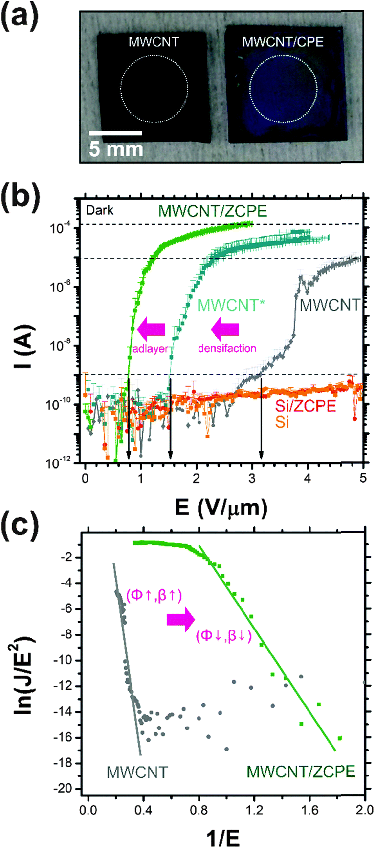 | ||
| Fig. 2 (a) Optical micrographs of typical Si/MWCNT (left) and Si/MWCNT/ZCPE (right) emitters. White dashed circles denote the extent of the system-fixed emission aperture (scale bar: 5 mm). (b) Current (I)–electric field (E) plots for the nascent MWCNTs (Si/MWCNTs), and the ZCPE coated MWCNTs (Si/MWCNT/ZCPE). Also shown are the control I–V plots for the underlying Si and the ZCPE coated Si (Si/ZCPE). Si/MWCNT* denotes emission from methanol treated, densified MWCNT forests. In all cases n = 3. Data points shown are the mean with the x, y error bars representing 1σ. (c) Corresponding Fowler–Nordheim plot for the Si/MWCNT and Si/MWCNT/ZCPE emitters. | ||
The ZCPE adlayer locally planarises the MWCNT surface whilst stimulating the formation of cracks within the MWCNT forests. The ZCPE also locally reduces the surface roughness of the exposed surfaces from 323 nm (MWCNT) to 134 nm (MWCNT/ZCPE), though we stress that this is only in the densified zones. High effective field enhancement factor, β is congruent with high surface RMS roughness. Thus, local planarization would suggest that β in these zones is reduced. Local smoothing is at the expense of crack formation within the MWCNT forest causing the global perturbation to increase. β will similarly increase given the significant perturbation in the emitter morphology following densification and global crack formation. Indeed, if we coarsely ascribe Fowler–Nordheim-like tunnelling,10,27 we find that the 〈β〉MWCNT = 3.51 (±0.27) × 103, 〈β〉MWCNT* = 4.10 (±0.57) × 104, and 〈β〉MWCNT/ZCPE = 3.99 (±0.29) × 104. The MWCNT* densified samples have a comparable field enhancement factor to the ZCPE coated devices, suggesting that crack formation in the adlayer has an analogous effect to the morphology changes in the MWCNT*. If field enhancement was the sole contributor to the observed improvement there would be negligible further difference between the ZCPE samples and the MWCNT* samples. This is not the case. Evidently the ZCPE plays a significant role in further reducing the turn-on field. It appears that the band structure at the emitter–vacuum interface plays a critical role in the observed enhancement; there is an evident inter-play between densification and the augmented band structure of the nanocomposite which results in the observed ultra-low turn-on fields.
Efficient field emission is widely correlated with low work functions. The work function (WF) of the MWCNTs was 5.0 eV, whilst the WF of the ZCPE coated MWCNTs was 3.61 (±0.23) eV. Work functions were measured using a Brueker Dimension Icon atomic force microscope operated in peak force Kelvin probe mode and equipped with a PFQNE-AL tip. All scan areas were 20 μm × 20 μm, with all means extracted for n = 256. Measured WFs were corroborated by room temperature photoemission spectroscopy, conducted in standard emission geometry. UPS measurements were conducted using He II radiation (hν = 40.8 eV) emitted from a conventional helium discharge lamp, with an overall energy resolution of ∼0.2 eV. The apparent WF reduction upon ZCPE coating could, at least in part, explain the observed enhanced field emission. The WF of the Si substrate was 4.32 (±0.01) eV, whilst the ZCPE-coated Si WF was 3.77 (±0.03) eV. A reduction of 1.39 eV in the WF of the cathode would, when taking into consideration the inferred β, suggests an increase in the FE current of between one and two orders of magnitude, which is broadly consistent with our empirical evidence. The I–E curves, shown in Fig. 2(c), fit with Fowler–Nordheim emission (MWCNT; R2 = 0.89, MWCNT/ZCPE; R2 = 0.81), however; it is likely that a more complex tunnelling model is required in order to fully explain the observed electron emission given the questionable applicability of Fowler–Nordheim for non-classical materials. There is, nonetheless, a possible dependence of the emission current on the surface work function, which, at least in part, goes some way towards capturing the mechanisms underpinning the observed electron emission. A number of transmission models have been proposed to date; emission based on triple junctions, in the case of diamond/metal/vacuum interfaces, has been proposed elsewhere,28 with some speculating that such a model may succinctly describe emission from the surface of polymer voids.21 It is also possible that the intrinsic potential drop across the polar ZCPE stimulates band bending resulting in shifted MWCNT–ZCPE and ZCPE–vacuum barriers, thereby augmenting the transmission probability. This intrinsic field may well stimulate a hot electron population, which creates a high transmission probability at the ZCPE/vacuum interface. We propose that the surface dipole effectively reduces the emitter–vacuum barrier thereby increasing the transmission efficiency at lower electric fields, as experimentally evidenced herein. Evidently the choice of ZCPE is critical in reducing the turn-on field. The polar side chains are important in forming a beneficial interfacial dipole. Indeed, our anionic polymer favours reduced turn-on fields, whereas a cationic ZCPE, such as those with nitrogen side groups, will likely increase the turn-on field. Data on which will be reported elsewhere.
Space charge cannot strictly be negated at the high current densities associated with high aspect ratio nano-tips. The gradient of the logI − logE provides a proxy for the dominant space charge-limiting current (SCLC) injection mechanism.21 In the high field regime (defined as the field necessary to stimulate an emission current >5 μA) we note a typical gradient of 9.97 for the MWCNTs, 2.23 for the MWCNT*, and 2.41 for the MWCNT/ZCPE. Conventionally, in a vacuum, Langmuir–Child29 SCLC is characterised by a gradient of 1.5, whereas Lampert–Rose, for bulk transport, suggested a gradient of at least 2.0.30 A gradient of ∼1.75 has been reported for nitrogenated diamond.31 Certainly, when considering our measured gradients for the MWCNT* and the MWCNT/ZCPE, there is a striking similarity to that of Lampert–Rose, though it is likely that this model only partly explains the observed barrier transmission, with the depopulation of local trap states, which themselves are expected to be optically, adding further complexity to the observed electron emission.
To further probe the transport mechanisms underpinning the observed reduction in Eon we have studied the emission performance as a function of optical excitation. DC optical exposure field emission measurements were acquired using six narrow band optical sources centred at (full-width at half maximum, FWHM); 208 nm (1.0 nm), 401.3 nm (4.8 nm), 442.6 nm (8.7 nm), 515.7 nm (38.5 nm), 655.0 nm (3.5 nm), 665.6 nm (13.9 nm), and 980.2 nm (5.6 nm). A broadband tungsten optical source was also employed, with a centre (FWHM) wavelength of 597 nm (255.6 nm). All optical sources had <5 mW incident power and were mounted exterior to the vacuum chamber. The chamber was optically isolated from ambient with the laser light passing through a quartz window. Spectra were acquired using an in situ mounted ASEQ Instruments LR1 spectrophotometer with a 1 nm resolution. Sample imagery was acquired using a long working distance microscope equipped with a ×200 objective. Sample temperature was monitored using a K-type bimetallic thermocouple. No sample heating was observed throughout. Typically, most cathode materials show a reduced Eon when exposed to low wavelength excitation, especially most metals. This is not the case for the MWCNT/ZCPE bilayer. The dependence of the maximum current (Imax) and turn-on field (Eon) on optical excitation wavelength (λ), for the MWCNT and MWCNT/ZCPE, is illustrated Fig. 3(a) and (b), respectively. For the MWCNTs, Eon and Imax appear largely invariant with optical excitation, as one would expect for the quasi-metallic MWCNTs. The Eon for the MWCNT/ZCPE samples tends to increase with decreasing wavelength, with a notable peak at λ ∼ 400 nm, spectrally consistent with the measured UV-vis absorption peak (Fig. 3(c)), with Imax showing a corresponding reduction. Optical transmission spectra were acquired on quartz supports using a Thermo Fisher UV-vis spectrometer operated from 190–1100 nm. Whilst the observed trend appears counter intuitive, one possible explanation for this could relate to the change in effective electrostatic diameter of the MWCNT/ZCPE with optical excitation. Optical excitation centred on the absorption peak stimulates a dramatic increase in the local free carrier concentration in the ZCPE adlayer. This manifestly increases the effective electrostatic diameter of the emitter, thereby reducing the emitters effective aspect ratio and, as a result, deleteriously increasing Eon. The polyfluorene backbone in our ZCPE is known to absorb photons in the visible range, resulting in the formation of surface excitons which interact with the local field,32 suggesting that the photoactive response of the MWCNT–(F(NSO3)2) interface plays a critical role in understanding the emission. For the MWCNT/ZCPE, at 400 nm, exciton formation in the ZPCE adlayer induces significant local charge transfer to the MWCNT scaffold which likely contributes to the observed deleterious increase in Eon. Evidently the interplay between the scaffold and the adlayer is significant in promoting field enhancement. The reduction in Imax between the optically excited and unexcited MWCNT/ZCPE samples, defined as the emission current at 1.1 kV in this instance, is a direct consequence of the increase in Eon.
 | ||
| Fig. 3 Maximum emission current (Imax) and turn-on electric field (Eon, defined as that required to stimulate an emission current of 1 nA) as a function optical excitation wavelength for (a) MWCNT, and (b) MWCNT/ZCPE. (c) Optical transmission spectra of the MWCNTs, ZCPE (FNSO3), and the MWCNT/ZPCE (MWCNT_FNSO3) composite. | ||
Direct measurement of the wavelength dependent carrier concentration in the present morphology is challenging. However, a good estimate for the carrier concentration in degenerate, quasi-metallic systems can be extracted from the modified Drude–Lorentz model, and associated Mie theory.33 In comparing the emission properties of the MWCNTs to the MWCNT/ZCPEs, if we consider the plasma frequencies in each case, approximated as the leading absorption edge for the MWCNTs and the absorption peak for the MWCNT/ZCPEs, we find that the ratio of plasma frequencies between the coated and uncoated samples is approximately equivalent to the square root of the ratio of the free carrier concentrations.34 Compared to the uncoated MWCNTs, we estimate a fourfold decrease in free carrier concentration at the upper most emission surface, following coating of the ZCPE adlayer when irradiated at 400 nm. This increases the effective electrostatic aspect ratio of the emitter by a factor of two (via a reduction in nearest neighbour shielding), assuming a purely radial augmentation in the effective emitter diameter. For a linear relationship between the field enhancement factor and the measured aspect ratio, of the form β ≈ (h/r), where h is the MWCNT height and r the MWCNT radius,35,36 one would expect that a halving of the effective emitter radius would approximately double β. An increase in β decreases Eon. Assuming a Fowler–Nordheim like emission profile, and a subsequent square-dependence on β, we would expect to note a reduction of at least a factor of four in Eon for the ZCPE-coated samples compared to the uncoated MWCNTs. Comparing this coarse estimate to our empirical data we do indeed find such a shift in Eon at the observed absorption peak.
Fig. 4(a) shows the DC time stability of the emission current, acquired at 4.00 V μm−1 over 24 hours, with a 10 s bias stabilising time for each measurement, under dark ambient, with each current averaged over 8 measurements. The MWCNT scaffold shows a typical variation, defined here as the relative standard deviation, in emission current of ±27%, consistent with the emission temporal stability from other graphitic nano-carbon allotropes.37,38 In contrast, the MWCNT/ZCPEs show a typical variation in current density of ±2%, which is, to the best of the authors' knowledge, one of the lowest reported DC stability measurements to date. The MWCNT/ZCPE shows a broadly similar variation in temporal stability to the MWCNTs, despite the considerably higher mean emission current, indicating that the mechanism is largely independent of the emission level – this clearly has substantial potential benefits. In situ residual gas analysis (RGA) highlighted the formation of higher order hydro carbon species (CxHy) during emission from the MWCNT/ZCPE samples, with this chemisorption process being largely invariant with optical excitation. Certainly our RGA findings suggest that the emitting surfaces of the MWCNTs and the MWCNT/ZCPE are vacuum stable via the absence of enhanced C peaks when comparisons are drawn between the spectra prior to, and during electron emission (Fig. S1, ESI†). In situ RGA was conducted using a computer controlled SRS Residual Gas Analyser (RGA 300), with 1 amu resolution operated from 1 to 100 amu.
 | ||
| Fig. 4 Temporal and spatial emission uniformity. (a) DC time stability of the MWCNT and MWCNT/ZCPE (measured at 4 V μm−1) showing a ±1.8% and ±26.7% temporal variation, respectively. Typical spatially-resolved (b and c) Von (defined as the bias needed to emit 1 nA). Values reported are the spatial average over the area inspected. (d and e) and Imax (defined as the emission current at 1.1 kV) for the MWCNT and the MWCNT/ZCPE, respectively (emitter-to-tip separation = 5 μm) (scale bars: 4 μm). (f) Modal comparison of the temporal (Δt) and spatial (Δx) variation in Imax. Schemes in the top left corners depict the measurement setup in each instance, where the red plate denotes the electron source (MWCNT/ZCPE), and the blue plate/tip representing the extraction electrode. | ||
While the MWCNTs provide the high-aspect ratio scaffold for the ZCPE adlayer the multiple peaks in the DC temporal stability histogram for the MWCNT/ZCPE samples may possibly be associated with the MWCNT support rather than the ZCPE adlayer directly. To probe the source of such instabilities, spatially resolved scanning anode field emission measurements (SAFEM) studies were performed. SAFEM measurements were conducted in a custom built ultra-high vacuum, ion pumped chamber operated at 10−8 mbar baked to 120 °C for 24 hours. Samples were measured in diode mode, with samples grounded and a KOH etched, W tip with a 100 nm diameter, held at a controlled distance adjacent to the sample. The tip was scanned in the z-direction using a UHV compatible piezo stage (Physik Instrumente P-601.4S piezo motor, equipped with a strain gauge sensor and with a maximum range of 400 μm and a resolution of 0.2 nm, controlled with an E-609 module). The sample was raster scanned in the x–y plane using two UHV compatible piezo stages with a minimum step size of 40 nm (Physik Instrumente LPS-45, fitted with integrated linear encoders, with a maximum range of ±13 mm and a minimum step of 40 nm, each controlled with an E-871.1A1 module). The tip was controllably positively biased from 0 to 1.1 kV using a source measure unit (Keithley 237) with the current monitored by the SMU and a redundant picoammeter (Keithley 485). Full diode I–V sweeps were acquired at each (x, y, z) coordinate. A sample-to-tip separation of 5 μm was used throughout. In excess of 110000 data points were collected during the measurement of each SAFEM map, with more than 41500 full I–V sweeps acquired throughout the study.
Fig. 4(b and c) shows a typical spatially resolved turn-on voltage, Von (defined as the bias needed to stimulate an emission current of 1 nA), and Fig. 4(d and e) the typical spatially resolved maximum current, Imax (measured at a bias of 1.1 kV), for the MWCNT and MWCNT/ZCPE samples, respectively. All MWCNT and MWCNT/ZCPE samples showed comparable absolute variation in Von and Imax, however; Von was some 10% lower for the ZCPE coated samples, with a corresponding near-three-fold increase in Imax. Fig. 4(f) depicts histograms of the nominal temporal (Δt) and spatial (Δx) variations in Imax for the MWCNT and MWCNT/ZCPE samples. The MWCNTs showed a bimodal Gaussian distribution, centred at 3.67 μA and 1.52 μA. Such bimodal line shapes suggest the possible dominance of two emission sites, a likely consequence of local heating and micro-plasma formation, as suggested in our in situ RGA studies. There is a similarity between the bimodal Gaussian line shape in both the Δt and Δx distributions, possibly supporting our notion that the observed temporal variations are correlated to the time-varied activation of new emission sites.
Fig. 5(a and b) show the variation in hysteresis behaviour of Imax as a function of cycle number for the MWCNT and the MWCNT/ZCPE emitters, respectively. Clear conditioning is evident for the MWCNT, with a near-linear (R2 = 0.80) shift in Imax of 0.18 (±0.02) μA per cycle. Though broader, the shift in Imax is extremely stable with cycle number for the MWCNT/ZCPE samples, suggesting that the entire emitter population is uniformly emitting with each cycle, whereas the MWCNTs show a clear positive-going shift in Imax with cycle number. Though arguably beneficial in the short-term, such evident conditioning will likely reduce the MWCNT emitters total lifetime relative to the MWCNT/ZCPE. To extend the emitter lifetime, pulsed-mode operation is widely employed. Pulsed field emission measurements were acquired using a half-bridge, push–pull high-voltage solid-state switch (Behlke HTS 61-03-GSM), rated at 6 kV with a maximum 90% turn-on time of 8 nS, driven by an 80 MHz Agilent 33250A function generator. The emission current was monitored using a 300 MHz Agilent DSO5032A oscilloscope. All pulsed measurements were conducted with a 50% duty-cycle with the measured currents representing an integrated current accumulated over 60 s. Pulsed emission experiments were conducted at 2 kV (inter-electrode separation, Δz = 500 μm) under dark ambient. The MWCNT/ZCPE samples allow for a bandwidth some 210% larger than the uncoated MWCNTs. As shown in Fig. 5(c), the high-frequency components of the transients leading edge evidently allow for an increase in the emission current density by a factor of up to 4.5 in the MWCNT/ZCPE case, and 10 for the MWCNTs, as similarly observed elsewhere.39 As shown in Fig. 5(d), at 5 kHz, the modulation depth (Imax − Imin) of the MWCNT/ZCPE cathodes was 27.0 (±0.2) μA, whilst the MWCNT emitters was 0.22 (±0.01) nA. The modulation depth of the MWCNT/ZCPE is significant, although the measurement parameters do not allow for a direct comparison between samples, as a result constant current pulsed measurements are under further investigation. The on-transient is likely a manifestation of the RC time delay associated with the measurement setup, rather than a fundamental limit associated with the transport. Nevertheless, though fundamentally cavity-limited, for the equivalent cathode geometry considered it is evident that the uncoated MWCNT emitters, compared to the ZCPE coated emitters, experience significantly more leading-edge ringing along with a reduced bandwidth of around half that for the ZCPE coated emitters.
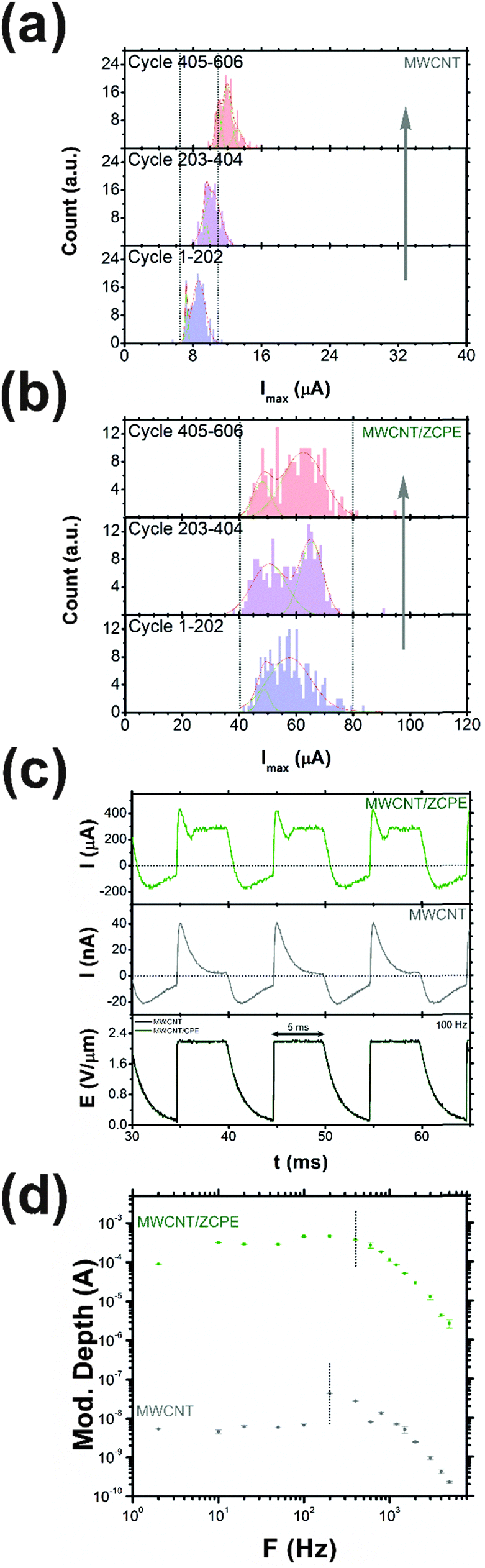 | ||
| Fig. 5 Emitter hysteresis and pulsed performance. Typical variation in SAFEM extracted Imax with sweep cycle number, for the (a) MWCNT and (b) MWCNT/ZCPE. (c) Example 100 Hz pulsed emission profiles from the MWCNT and the MWCNT/ZCPE emitters, and (d) the corresponding device bandwidth. | ||
Conclusions
Here we have shown that anionic conjugated polyelectrolytes present a unique class of field electron emission enhancing adlayers that have many particular merits when coupled to high aspect ratio nanomaterials, such as multi-walled carbon nanotubes. The zwitterionic polyelectrolyte has here, for the first time, been shown to dramatically reduce the turn-on electric field of nascent MWCNTs by around 66% whilst having a potentially beneficial impact on the temporal and long-term cyclic stability. This notable reduction is also coupled to an order of magnitude increase in maximum emission current suggesting that engineered polar molecules may, when coupled to novel carbon allotropes, allow for a straightforward and readily adopted route towards high current density electron sources.Conflict of interest
The authors declare no competing financial interest.Acknowledgements
We thank Wilhem Huck (Department of Chemistry, Cambridge University) for the ZCPE synthesis. M. T. C. thanks the Oppenheimer Trust for generous financial support. This work was supported by the Engineering and Physical Sciences Research Council Cambridge Nano Doctoral Training Centre (EP/L015978/1), an Engineering and Physical Sciences Research Council Impact Acceleration Account, and an Advanced Materials grant from Innovate UK.References
- R. Parmee, W. I. Milne and M. T. Cole, X-ray Generation Using Carbon Nanotubes, NanoConvergence, 2015, 2, 1, DOI:10.1186/s40580-014-0034-2.
- N. De Jonge and J. M. Bonard, Carbon Nanotube Electron Sources and Applications, Philos. Trans. R. Soc., A, 2004, 362, 2239–2266 CrossRef CAS PubMed.
- W. I. Milne, K. B. K. Teo, G. A. J. Amaratunga, P. Legagneux, L. Gangloff, J. P. Schnell, V. Semet, V. T. Binh and O. Groening, Carbon Nanotubes as Field Emission Sources, J. Mater. Chem., 2004, 14, 933–943 RSC.
- E. F. Barasch, H. P. Demroff, T. S. Elliott, T. B. Kasprowicz, B. Lee, T. Mazumdar, P. M. Mcintyre, Y. Pang, D. D. Smith, H.-J. Trost, in Gated Field-Emitter Cathodes for High-Power Microwave Applications, Proceedings of the 1992 Linear Accelerator Conference, Ottawa, Ontario, Canada, 1992.
- M. T. Cole, W. I. Milne and M. Nakamoto, in Handbook of Digitial Imaging – Field Emission Displays (Fed) & Surface-Conduction Electron-Emitter Displays (Sed), ed. M. Kriss, John Wiley & Sons Ltd, London, 2014, vol. 1 Search PubMed.
- I. Shah, Field-Emission Displays, Phys. World, 1997, 45–50 CrossRef CAS.
- H. P. Schlenvoigt, K. Haupt, A. Debus, F. Budde, O. Jackel, S. Pfotenhauer, H. Schwoerer, E. Rohwer, J. G. Gallacher and E. Brunetti, et al. A Compact Synchrotron Radiation Source Driven by a Laser-Plasma Wakefield Accelerator, Nat. Phys., 2008, 4, 130–133 CrossRef CAS.
- M. T. Cole, C. Collins, R. Parmee, C. Li and W. I. Milne, Nanocarbon Electron Emitters: Advances & Applications, in Chemical Functionalisation of Carbon Nanomaterials: Chemistry & Applications – Structure & Synthesis, Taylor & Francis, 2015 Search PubMed.
- M. T. Cole, C. Li, Y. Zhang, S. G. Shivareddy, J. S. Barnard, W. Lei, B. Wang, D. Pribat, G. A. J. Amaratunga and W. I. Milne, Hot Electron Field Emission Via Individually Transistor-Ballasted Carbon Nanotube Arrays, ACS Nano, 2012, 6, 3236–3242 CrossRef PubMed.
- M. T. Cole, K. B. K. Teo, O. Groening, L. Gangloff, P. Legagneux and W. I. Milne, Deterministic Cold Cathode Electron Emission from Carbon Nanofibre Arrays, Sci. Rep., 2014, 4, 4840, DOI:10.1038/srep04840.
- Y. Chen, H. Jiang, D. Li, H. Song, Z. Li, X. Sun, G. Miao and H. Zhao, Improved Field Emission Performance of Carbon Nanotube by Introducing Copper Metallic Particles, Nanoscale Res. Lett., 2011, 6, 537 CrossRef PubMed.
- Y. M. Chen, C. A. Chen, Y. S. Huang, K. Y. Lee and K. K. Tiong, Characterization and Enhanced Field Emission Properties of Iro 2 -Coated Carbon Nanotube Bundle Arrays, Nanotechnology, 2010, 21, 035702 CrossRef CAS PubMed.
- M. Kumari, S. Gautam, P. V. Shah, S. Pal, U. S. Ojha, A. Kumar, A. A. Naik, J. S. Rawat, P. K. Chaudhury and Harsh, et al. Improving the Field Emission of Carbon Nanotubes by Lanthanum-Hexaboride Nano-Particles Decoration, Appl. Phys. Lett., 2012, 101, 123116, DOI:10.1063/1.4754110.
- L. Kun, C. Ming-Ju, L. Hua-Yang, L. Er-Jun and Y. Bin, Comparison of Field Emission in Carbon Nanotubes and Gallium-Doped Carbon Nanotubes, Journal of Inorganic Materials, 2007, 22, 181–184 Search PubMed.
- J. Lee, T. Park, J. Lee, S. Lee, H. Park and W. Yi, Electric Field Enhancements in In2O3-Coated Single-Walled Carbon Nanotubes, Carbon, 2014, 76, 378–385 CrossRef CAS.
- S. Y. Lee, W. C. Choi, C. Jeon, C.-Y. Park, J. H. Yang and M. H. Kwon, Field Emitter Density Control Effect on Emission Current Density by Ag–Cu Alloy Coating on Carbon Nanotubes, Appl. Phys. Lett., 2008, 93, 103101, DOI:10.1063/1.2972120.
- C. Li, Y. Zhang, M. Mann, P. Hiralal, H. E. Unalan, W. Lei, B. P. Wang, D. P. Chu, D. Pribat and G. A. J. Amaratunga, et al. Stable, Self-Ballasting Field Emission from Zinc Oxide Nanowires Grown on an Array of Vertically Aligned Carbon Nanofibers, Appl. Phys. Lett., 2010, 96, 143114 CrossRef.
- Z. D. Lin, Y. Sheng-Joue, H. Chih-Hung, C. Shoou-Jinn and C. S. Huang, Improved Field Emission Properties of Ag-Decorated Multi-Walled Carbon Nanotubes, IEEE Photonics Technol. Lett., 2013, 25, 1017–1019 CrossRef CAS.
- C. Liu, K. S. Kim, J. Baek, Y. Cho, S. Han, S.-W. Kim, N.-K. Min, Y. Choi, J.-U. Kim and C. J. Lee, Improved Field Emission Properties of Double-Walled Carbon Nanotubes Decorated with Ru Nanoparticles, Carbon, 2009, 47, 1158–1164 CrossRef CAS.
- S. K. Pillai, S. C. Motshekga, S. S. Ray and J. Kennedy, Field Emission Characteristics of SnO2/Cnts Composites Prepared by Microwave-Assisted Wet Impregnation, J. Nanomater., 2012, 2012, 861591, DOI:10.1155/2012/861591.
- I. Musa, D. A. I. Munindrasdasa, G. A. J. Amaratunga and W. Eccleston, Ultra-Low-Threshold Field Emission from Conjugated Polymers, Nature, 1998, 395, 362–365 CrossRef CAS.
- J. Fang, B. H. Wallikewitz, F. Gao, G. Tu, C. Müller, G. Pace, R. H. Friend and W. T. S. Huck, Conjugated Zwitterionic Polyelectrolyte as the Charge Injection Layer for High-Performance Polymer Light-Emitting Diodes, J. Am. Chem. Soc., 2011, 133, 683–685 CrossRef CAS PubMed.
- A. Kumar, G. Lakhwani, E. Elmalem, W. T. S. Huck, A. Rao, N. C. Greenham and R. H. Friend, Interface Limited Charge Extraction and Recombination in Organic Photovoltaics, Energy Environ. Sci., 2014, 7, 2227–2231 CAS.
- G. Zhong, J. H. Warner, M. Fouquet, A. W. Robertson, B. Chen and J. Robertson, Growth of Ultrahigh Density Single-Walled Carbon Nanotube Forests by Improved Catalyst Design, ACS Nano, 2012, 6, 2893–2903 CrossRef CAS PubMed.
- S. Esconjauregui, M. Fouquet, B. C. Bayer, C. Ducati and J. Robertson, Catalyst Design for the Growth of Highly Packed Nanotube Forests, Phys. Status Solidi B, 2011, 248, 2528–2531 CrossRef CAS.
- Y. Zou, P. W. May, S. M. C. Vieira and N. A. Fox, Field Emission from Diamond-Coated Multiwalled Carbon Nanotube “Teepee” Structures, J. Appl. Phys., 2012, 112, 044903, DOI:10.1063/1.4748336.
- M. T. Cole, K. Hou, J. H. Warner, J. S. Barnard, K. Ying, Y. Zhang, C. Li, K. B. K. Teo and W. I. Milne, In-Situ Deposition of Sparse Vertically Aligned Carbon Nanofibres on Catalytically Activated Stainless Steel Mesh for Field Emission Applications, Diamond Relat. Mater., 2012, 23, 66–71 CrossRef CAS.
- M. W. Geis, N. N. Efremow, K. E. Krohn, J. C. Twichell, T. M. Lyszczarz, R. Kalish, J. A. Greer and M. D. Tabat, A New Surface Electron-Emission Mechanism in Diamond Cathodes, Nature, 1998, 393, 431–435 CrossRef CAS.
- W. A. Anderson, Role of Space Charge in Field Emission Cathodes, J. Vac. Sci. Technol., B: Microelectron. Nanometer Struct.–Process., Meas., Phenom., 1993, 11, 383–386 CrossRef CAS.
- M. A. Lampert and P. Mark, Current Injection in Solids, New York, 1970, pp. 44–46 Search PubMed.
- G. A. J. Amaratunga and S. R. P. Silva, Nitrogen Containing Hydrogenated Amorphous Carbon for Thin-Film Field Emission Cathodes, Appl. Phys. Lett., 1996, 68, 2529–2531 CrossRef CAS.
- A. Kumar, G. Pace, A. A. Bakulin, J. Fang, P. K. H. Ho, W. T. S. Huck, R. H. Friend and N. C. Greenham, Donor-Acceptor Interface Modification by Zwitterionic Conjugated Polyelectrolytes in Polymer Photovoltaics, Energy Environ. Sci., 2013, 6, 1589–1596 CAS.
- J. M. Luther, P. K. Jain, T. Ewers and A. P. Alivisatos, Localized Surface Plasmon Resonances Arising from Free Carriers in Doped Quantum Dots, Nat. Mater., 2011, 10, 361–366 CrossRef CAS PubMed.
- M. Saha, S. Ghosh, V. D. Ashok and S. K. De, Carrier Concentration Dependent Optical and Electrical Properties of Ga Doped Zno Hexagonal Nanocrystals, Phys. Chem. Chem. Phys., 2015, 17, 16067–16079 RSC.
- M. Jha, R. Patra, S. Ghosh and A. K. Ganguli, Vertically Aligned Nanorods of Lanthanum Hexaboride with Efficient Field Emission Properties, Solid State Commun., 2013, 153, 35–39 CrossRef CAS.
- K. L. Ng, J. Yuan, J. T. Cheung and K. W. Cheah, Electron Field Emission Characteristics of Electrochemical Etched Si Tip Array, Solid State Commun., 2002, 123, 205–207 CrossRef CAS.
- S. Fan, M. G. Chapline, N. R. Franklin, T. W. Tombler, A. M. Cassell and H. Dai, Self-Oriented Regular Arrays of Carbon Nanotubes and Their Field Emission Properties, Science, 1999, 283, 512–514 CrossRef CAS PubMed.
- J. M. Bonard, J. P. Salvetat, T. Stockli, W. A. de Heer, L. Forro and A. Chatelain, Field Emission from Single-Wall Carbon Nanotube Films, Appl. Phys. Lett., 1998, 73, 918–920 CrossRef CAS.
- F.-G. Zeng, X. Li, L. Xia and R. Zhang, Intense Pulsed Field Emission of Carbon Nanotube Film Grown on Electroless Plated Nickel Substrate by Pyrolysis, Phys. Status Solidi C, 2012, 9, 74–76 CrossRef CAS.
Footnotes |
| † Electronic supplementary information (ESI) available: Fig. S1. In situ residual gas analysis of the chamber ambient during electron emission, as a function of optical excitation for (a) MWCNT and (b) MWCNT/ZCPE. See DOI: 10.1039/c6nh00071a |
| ‡ Authors contributed equally. |
| This journal is © The Royal Society of Chemistry 2016 |