
 Open Access Article
 This Open Access Article is licensed under a
 Creative Commons Attribution 3.0 Unported Licence
An electrode design rule for high performance top-illuminated organic photovoltaics†
Martin S.
Tyler
,
Immad M.
Nadeem‡§
and
Ross A.
Hatton
*
Department of Chemistry, University of Warwick, CV4 7AL, UK. E-mail: Ross.Hatton@warwick.ac.uk
First published on 9th May 2016
Abstract
An electrode design rule for high performance top-illuminated bulk-heterojunction organic photovoltaics is proposed, that enables the device architecture to be simplified by removing the need for the electron selective layer at the interface with the low work function reflective electrode. This new guideline for electrode design is underpinned by device studies in conjunction with a study of the energetics at the interface between five widely used solution processed organic semiconductors of both electron donor and acceptor type, and a stable low work function reflective substrate electrode. The magnitude and distribution of space charge resulting from ground-state electron transfer from the electrode into each organic semiconductor upon contact formation is derived from direct measurements of the interfacial energetics using the Kelvin probe technique, which enables the variation in potential across the entire film thickness used in the devices to be probed.
Conceptual insightsWe show a new design rule for top-illuminated organic photovoltaics (OPVs) that enables the device structure to be simplified by removing one of the charge selective layers and thereby offers a path to lower fabrication cost. OPVs based on a solution processed bulk-heterojunction offer the lowest cost path to the fabrication of OPVs. For these devices it is considered essential to include charge selective layers at both electrode interfaces, since both the donor and acceptor phases of the bulk-heterojunction can contact both electrodes. In this communication we show, through a combination of device studies and a study of the energetics at the interface between five widely used solution processed organic semiconductors (of both electron donor and acceptor type) and a low work function reflective substrate electrode, that for top-illuminated OPVs the hole-blocking layer is not needed when the donor material has a narrow bandgap – a requirement that is easily met in high performance donor polymers. Additionally, to our knowledge, these are the first reported measurements of the energetics between such a low work function substrate electrode and solution processed organic semiconductors, uncomplicated by the uncontrolled chemical reaction that usually occurs at the interface with low work function electrodes. |
Introduction
It is widely accepted that organic photovoltaics (OPVs) based on a solution processed bulk-heterojunction (BHJ) of electron donor and electron acceptor type organic semiconductors offer the lowest cost path to the fabrication of OPVs.1 For this type of OPV it is considered essential to include wide band gap charge extraction layers at both electrode interfaces to ensure optimised interfacial energetics and guarantee charge carrier selectivity, since both donor and acceptor type organic semiconductors can contact both electrodes.2,3 The thickness of these charge extraction layers is typically in the range 3–50 nm,4–9 sufficient to block the extraction of one carrier type whilst at the same time not significantly contributing to device series resistance or parasitic absorption of incident light. For hole-blocking layers (HBLs) the wideband gap oxides ZnOx and TiOx are the materials of choice because they can be deposited from solvents that are orthogonal to those used for organic semiconductors and have the deep lying valance band edge needed to block unwanted hole-extraction by the electrode, a process that erodes device fill factor (FF) and short-circuit current density (Jsc).4,10 These materials are n-type with a conduction band edge at comparable energy to the lowest unoccupied molecule orbital (LUMO) in the electron-acceptor component of the BHJ, and so serve to align the electrode Fermi level to the LUMO of the organic electron-acceptor which maximises the electric field strength across the BHJ. The use of these metal oxides removes the need for a low work function reactive metal electrode such as Ca because they can be used in conjunction with relatively high work function, and thus relatively stable metals such as Ag.7,11 It has been proposed that these wide band gap interfacial layers also offer the benefit of: (i) reduced quenching of excitons formed in the BHJ near to the reflective electrode, leading to improved Jsc;12 and (ii) increased Jsc by acting as an optical spacer layer, which enables tuning of the optical field distribution to maximise absorption of light.13Increasingly OPVs with a top-illuminated architecture are attracting attention because they remove the need for costly conducting oxide coated glass and increase the range of potential applications by giving more flexibility in terms of the materials used as the supporting substrate.8,13–15 In this class of OPV the preferred location of the HBL is at the contact with the reflective substrate electrode, which has proved to be the most stable device architecture.16 The potential benefit of an optical spacer at the interface with the reflective electrode in top-illuminated OPVs has been explored by Lin et al.17 in the context of OPV devices based on very thin films of evaporated small molecule organic semiconductors. However, the thickness of the optical spacer layer needs to be very carefully controlled and this approach is only useful for a narrow range of incident angles, so is not a panacea for light management in top-illuminated OPVs.11
Herein we present the results of a study of the energetics at the interface between five widely used solution processed organic semiconductors and a low work function (∼3.25 eV) electrode, in conjunction with OPV device studies, and use this data to under-pin a new electrode design rule for top-illuminated OPVs. To our knowledge the vast majority of published reports to date relating to the study of energy level alignment at the interface between substrate electrodes and solution processed organic semiconductors have been limited to relatively high work function (≥3.8 eV) electrode materials,18a–c or electrodes capped with an HBL such as ZnOx,19,20 likely due to the difficultly of working with low work function metals outside of a vacuum system. We have recently reported a means of rendering Al films sufficiently stable towards oxidation for practical application as a substrate electrode in top-illuminated OPVs, using a very thin capping layer of Cu and Al.21 This triple layer metal electrode is well-matched to the requirements of top-illuminated OPVs because it offers the advantages of high reflectivity, low metal cost, and the rare combination of high stability towards oxidation and a very low work function; 3.25 eV ± 0.08 eV.21 In the current study we have exploited this new reflective electrode, which presents an opportunity to investigate the energetics at the interface between a low work function electrode and solution processed organic semiconductor junction without the complexity associated with interfacial chemical reaction and uncontrolled oxidation.
Experimental
Glass substrates were thoroughly cleaned using a four stage process with ultra-sonic agitation in: (i) deionised water/surfactant (Decon, Neutracon) solution; (ii) deionised water; (iii) isopropanol; (iv) and finally acetone vapour, followed by blow drying with nitrogen. Substrates were then UV/O3 treated to remove surface organic contaminants.All sample fabrication and testing was carried out in a N2 filled glove box with a base O2 level of <3 ppm unless otherwise stated. Evaporation of metals was carried out using a CreaPhys Organic molecular evaporator co-located in the same glovebox as the spin coater. The thickness of all vacuum deposited layers was measured using a calibrated quartz-crystal microbalance (QCM) mounted adjacent to the substrates. All metals were thermally evaporated using tungsten boats. MoO3 was thermally evaporated from boron nitride crucibles. The working pressure of the system was ≤1 × 10⁻⁵ mbar. To fabricate the reflective electrodes onto cleaned 12 × 12 mm2 glass slides was thermally evaporated Al (60–100 nm, 1 nm s−1), Cu (8 nm, 0.1 nm s−1), Al (0.8 nm, 0.01–0.03 nm s−1) without breaking the vacuum between depositions followed by oxidation in dry air for 1 hour, as previously reported,20 to ensure oxidation of the thin capping layer.
Organic semiconductor films of increasing thickness were deposited from solutions fabricated using the spin coating technique with concentrations and spin speeds as follows; [6,6]-phenyl-C71-butyric acid methyl ester (PC70BM) in CHCl3 (24, 12, 6, 3, 1, 0.2 mg ml−1) spin cast, slide spun initially then solution applied, at 6000 rpm for 60 s followed by annealing at 80 °C for 30 min; [6,6]-phenyl-C61-butyric acid methyl ester (PC60BM) in CHCl3 (24, 12, 6, 0.5 mg ml−1) spin cast at 6000 rpm for 60 s followed by annealing at 80 °C for 30 min; poly({4,8-bis[(2-ethylhexyl)oxy]benzo[1,2-b:4,5-b′]dithiophene-2,6-diyl}{3-fluoro-2-[(2-ethylhexyl)carbonyl]thieno[3,4-b]thiophenediyl}) (PTB7; Mn 10![[thin space (1/6-em)]](https://www.rsc.org/images/entities/char_2009.gif) 500 g ml−1; Mw 18000 g mol−1; PDI 1.75) in 1,2-dichlorobenzene (DCB) (10, 5, 2.5, 1 mg ml−1) drop cast, solution applied before spinning, at 1000 rpm for 60 s dried under vacuum for 1 h; poly(3-hexylthiophene-2,5-diyl) (P3HT; Mw 50000–60000 g mol−1; PDI 1.8–2.2) in DCB (20, 10, 5, 1 mg ml−1) drop cast then spun at 1000 rpm for 120 s followed by 30 min under N2 then annealed at 120 °C for 30 min, poly[N-9′-heptadecanyl-2,7-carbazole-alt-5,5-(4′,7′-di-2-thienyl-2′,1′,3′-benzothiadiazole)] (PCDTBT; Mn 17000 g ml−1; Mw 36000 g mol−1; PDI 2.15) in CHCl3 (4, 2, 1 mg ml−1) drop cast then spun at 1000 rpm for 60 s or spin cast at 6000 or 3000 rpm all then annealed at 80 °C for 30 min.
500 g ml−1; Mw 18000 g mol−1; PDI 1.75) in 1,2-dichlorobenzene (DCB) (10, 5, 2.5, 1 mg ml−1) drop cast, solution applied before spinning, at 1000 rpm for 60 s dried under vacuum for 1 h; poly(3-hexylthiophene-2,5-diyl) (P3HT; Mw 50000–60000 g mol−1; PDI 1.8–2.2) in DCB (20, 10, 5, 1 mg ml−1) drop cast then spun at 1000 rpm for 120 s followed by 30 min under N2 then annealed at 120 °C for 30 min, poly[N-9′-heptadecanyl-2,7-carbazole-alt-5,5-(4′,7′-di-2-thienyl-2′,1′,3′-benzothiadiazole)] (PCDTBT; Mn 17000 g ml−1; Mw 36000 g mol−1; PDI 2.15) in CHCl3 (4, 2, 1 mg ml−1) drop cast then spun at 1000 rpm for 60 s or spin cast at 6000 or 3000 rpm all then annealed at 80 °C for 30 min.
In order to deposit a ZnOx layer from solution the proven low temperature method described by Jagadamma et al.4 was used: ZnOx HBL zinc acetate dihydrate (0.08 M) and ethanolamine (0.08 M) were added to 2-methoxyethanol and stirred in air for 12 hours prior to use. A 5 nm film was then formed by drop casting the solution followed by spinning at 4000 rpm for 60 seconds and annealing at 100 °C for 10 minutes in air. This method has been shown to result in compact ZnOx films compatible with processing on flexible plastic or oxidisable substrates, and offers the advantage of reduced cost as compared to high temperature processing.4,5,22
BHJ solutions were prepared as follows: PTB7:PC70BM (1:1.5) was dissolved at a concentration of 25 mg ml−1 in DCB:diiodotane (97:3 vol%) followed by stiring at 60 °C for 1 h then heating at 40 °C for 17 h; P3HT:PC60BM solution (1:1) was prepared by dissolving 40 mg ml−1 in DCB followed by stirring at 45 °C for 1 week prior to use. Both BHJ solutions were filtered through a 0.2 μm PTFE filter prior to use.
OPV devices were fabricated by thermally evaporating Al|Cu|Al electrodes as above. ZnOx was deposited as above followed by spin coating of either PTB7:PC70BM solution (drop cast at 1000 rpm for 60 s then 6000 rpm for 4 s followed by 30 min drying in N2) or P3HT:PC60BM solution (drop cast at 600 rpm for 120 s followed by 45 min drying in N2 then annealed at 120 °C for 20 min). MoO3 (5 nm, 0.04 nm s−1) and Ag (11 nm, 0.2 nm s−1) were then thermally evaporated to form the top window electrode. JV curves were measured using a Keithley 2400 source-meter under AM1.5G solar illumination at 100 mW cm−2 (1 Sun). External quantum efficiency (EQE) and reflectance measurements were carried out using a Sciencetech SF150 xenon arc lamp and a PTI monochromator, with the monochromatic light intensity calibrated using a Si photodiode (Newport 818-UV). The incoming monochromatic light was chopped at 500 Hz. For signal measurement a Stanford Research Systems SR 830 lock-in amplifier was used. Tapping mode Atomic Force Microscopy (AFM) imaging was performed in air using an Asylum Research MFP3D. Work function measurements were performed using a Kelvin probe referenced to freshly cleaved highly oriented pyrolytic graphite in a nitrogen-filled glove box co-located with the thermal evaporator.
Differential pulse voltammetry was conducted in dichloromethane with 0.1 M tetrabutylammonium hexafluorophosphate electrolyte with μM concentrations of PC60BM and PC70BM. CH Instruments Electrochemical Analyzer was used with a platinum working electrode, a Ag/AgCl reference electrode and platinum wire as the counter electrode. HOMO and LUMO levels are calculated as shown in ESI† with the method proposed by D'Andrade et al.23 and Djurovich et al.24 respectively.
Results & discussion
To probe the interfacial energetics upon contact formation the Kelvin probe technique20,25 was used to measure the change in energy of the vacuum level (εvac) relative to the Fermi level (εF), denoted as εvacF, upon deposition of organic semiconductor layers from solution onto Al|Cu|Al electrodes. Importantly, measurements were made under nitrogen immediately after organic semiconductor deposition without exposure to the laboratory atmosphere. Unlike ultra-violet photo-electron spectroscopy, which is most widely used to make measurements of interfacial energetics, the maximum film thickness that can be probed using the Kelvin probe technique is not limited by sample charging.20,26–29 As a result, the change in potential across film thicknesses comparable to that used in OPV devices can be probed. Measurements were made for two archetypal electron acceptors; PC70BM and PC60BM (Fig. 1), and three widely used electron donors; PCDTBT, PTB7, and P3HT (Fig. 2) (full chemical names given in Experimental). Uniform thin films of these materials were deposited by spin coating whilst the thickness was tuned via the solution concentration (0.1–24 mg ml−1) and spin speed. Film thickness was measured by scoring the film to form a step and measuring the step height using AFM (ESI,† Fig. S1).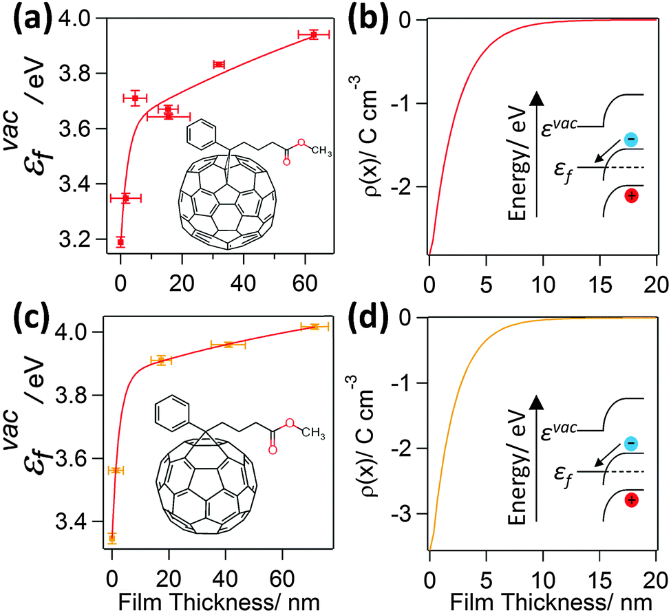 | ||
| Fig. 1 (a) and (c) show the variation in εvacF for PC70BM and PC60BM films supported on an Al|Cu|Al electrode. The εvacF data is fitted with a double exponential function. The insets show the corresponding structures of the molecules; (b and d) show the space charge density distribution, ρ(x), calculated using eqn (1), that would give rise to the measured variation in potential. | ||
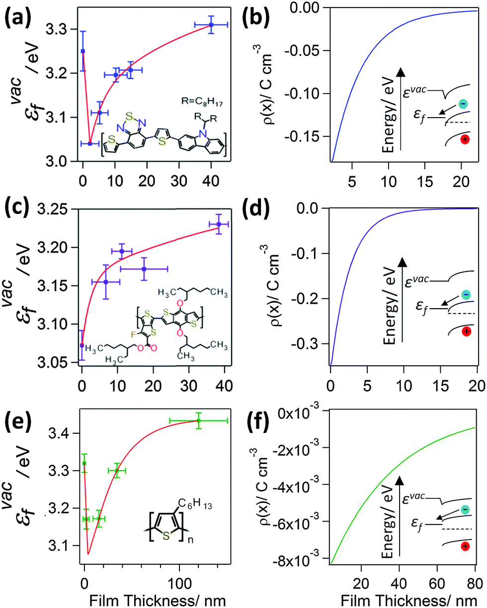 | ||
| Fig. 2 Variation in εvacF (a), (c) and (e) and charge distribution (b), (d) and (f) for donor organic semiconductor thin films supported on an Al|Cu|Al electrode as a function of semiconductor film thickness for: PCDTBT (a) and (b); PTB7 (c) and (d); and P3HT (e) & (f). The insets show the corresponding structures of the molecules and schematic energy level diagrams. The εvacF data is fitted with a double exponential function. For the cases of PCDTBT and P3HT, for which the push back effect is observed, the total space charge was calculated for thicknesses after the initial abrupt decrease in the εvac. | ||
It is evident from Fig. 1(a) and (c) that for both PC70BM and PC60BM films there is a ∼0.7 eV increase in εvacF across the thickness of the fullerene layers, most of which occurs within the first 10 nm of the interface. In both cases the change is consistent with spontaneous transfer of electron density from the electrode into the adjacent fullerene layer, giving rise to a static space charge region near to the interface and band bending, as depicted in Fig. 1(b) and (d). For each of the measurements of interfacial energetics the space charge distribution ρ(x) that would give rise to the measured variation in potential is calculated using Poisson's equation:
 | (1) |
In the context of a BHJ OPV both the donor and acceptor phases can have an interface with both electrodes, and so it is interesting to consider the energetics at the contact between the donor type organic semiconductor and the low work function electrode, a class of interface that has been sparsely investigated to date and only in the context of vacuum deposited small molecules.26,32,33 It is evident from Fig. 2(a), (c) and (e) that the extent of electron transfer from the Al|Cu|Al electrode into the three donor type semiconductors investigated is much less than that at the interface with the fullerenes, which is consistent with the shallower LUMO states in donor type organic semiconductors.3 For both PTB7 and PCDTBT the LUMO is below the Fermi level of the electrode at 3.3–3.5 eV34,35 and 3.4–3.6 eV36,37 below εvac respectively, so there is a high density of empty states into which electron density can be accepted. Consequently, most of the potential energy change occurs very close to the electrode in both of these cases, just as for the fullerenes. Conversely, the rate of change in potential energy with distance from the electrode in the P3HT film is much more gradual and occurs over a much greater film thickness, due to the shallow LUMO of P3HT; only ∼3.0 eV below εvac.38,39 The LUMO of P3HT is in fact above the Fermi level of the electrode and so the electron density transferred – which is motivated by the difference in chemical potential – must be accommodated in defect states in the P3HT bandgap. Since the density of unintentional electron accepting defects states in the band gap of P3HT is expected to be relatively low, due to the high purity of the polymers used in this study,40 band bending is much more gradual than for PTB7 and PCDTBT. Crucially, high performance donor-type polymers are invariably characterised by a narrower band gap than P3HT (<1.8 eV vs. ≥2.0 eV) and a larger ionisation potential (≥5.2 eV vs. ≤5.0 eV),34–37,39,41,42 the latter of which ensures the highest occupied molecular orbital (HOMO) energy is sufficiently deep lying to achieve a large open-circuit voltage (Voc).43 Consequently the LUMO in high performance donor type polymers is, by design, much lower lying than in P3HT, and so the pictures of the interfacial energetics at the interface with PTB7 and PCDTBT shown in Fig. 2(a) and (c) are most representative of the energetics that would be achieved at the interface between the low work function electron-extracting electrode and a high performance narrow band gap donor-type polymer in the absence of a HBL.
As is evident from Fig. 1 and 2, all of the organic semiconductor films accept electron density from the low work function electrode. Notably, for the cases of PCDTBT and P3HT (Fig. 2(a) and (e)) there are two distinct parts to the change in εvacF; an initial sharp decrease in εvacF followed by the aforementioned more gradual increase. The latter occurs over a film thickness equivalent to the first few molecular layers of the organic semiconductor. This effect – which has been widely documented to occur at the interface between vacuum deposited small organic molecule films, although sparsely reported at the interface between electrodes and solution processed organic semiconductors – is attributed to the pushback effect, which results from a reduction in the size of the dipole layer at the surface of the electrode rather than charge transfer from the organic semiconductor layer into the electrode.29 Using Poisson's equation (eqn (1)) the average space charge density in each of the organic semiconductors within 5 nm of the interface is calculated to be: PC70BM; −1.2 C cm−3, PC60BM; −1.5 C cm−3, PCDTBT; −0.11 C cm−3, PTB7; −0.16 C cm−3, and P3HT; −7.3 × 10⁻³ C cm−3, which are all much greater than the space charge density associated with the photocurrent in high performance OPVs. For example, the hole density at the short-circuit condition under 1 Sun illumination in an OPV based on PTB7:PC70BM is estimated to be 4–5 × 10⁻⁴ C cm−3 assuming a photocurrent of 12–15 mA cm−2 and the charge carrier mobilities reported by Ebenhoch et al.40 This is three orders of magnitude lower than that formed at the interface due to spontaneous ground state electron transfer, and so it can be concluded that this space charge distribution in the PTB7 phase persists under illumination, and the energy level diagram depicted in Fig. 2(d) is a true picture of the energetics close to the interface in a working device. For the case of P3HT:PC60BM OPVs the space charge density due to current flow can be as high as 1.7 × 10⁻³ C cm−3 in optimised devices44 (assuming the charge carrier mobilities from Huang et al.45), which is much closer to the space charge density formed at the interface due to spontaneous ground state electron transfer, although is still several times smaller. Based on these measurements we propose that for BHJ OPVs using high performance donor type materials in conjunction with a low work function reflective electrode, there is no need for a HBL because the spontaneous formation of a Schottky-type junction in both donor and acceptor phases serves to favour efficient electron-extraction whilst blocking unwanted hole-extraction.
To test the proposed design rule we have fabricated efficient top-illuminated OPVs using the Al|Cu|Al electrode as the electron extracting back reflective electrode with and without a thin ZnOx HBL. In order to disentangle optical effects from electronic effects, which is challenging for high performance OPVs based on very thin photoactive layers, we have used a very thin ZnOx film of 5 nm ± 1.7 nm. As shown in Fig. 3(a) and Table 1, PTB7 OPVs with and without a ZnOx HBL have virtually identical Jsc, Voc and FF, indicating that the electron-selective function of the ZnOx interlayer is not-needed in that case. The external quantum efficiency (EQE) (Fig. 3(b)) of the OPVs with and without the ZnOx does however exhibit a small mismatch which, based on the results of the optical simulations shown in Fig. 3(c) and (d) can be attributed to slight differences in the optical field distribution in the device. At shorter wavelengths (∼350 nm) there is however no difference in the photo-response with or without an HBL, which is corroborating evidence that the ZnOx film is not needed.
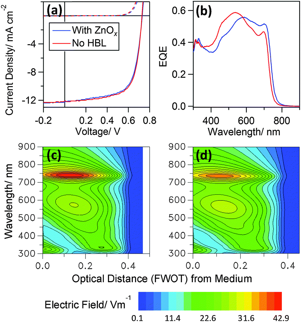 | ||
| Fig. 3 Performance characteristics of OPV devices with the structure: Al (70 nm)|Cu (8 nm)|Al (0.8 nm)|ZnOx (5 nm)|PTB7:PC70BM|MoO3 (5 nm)|Ag (11 nm) with and without a ZnOx HBL: (a) JV characteristics in the dark (dashed line) and under 1 Sun illumination (continuous line). (b) Corresponding EQE spectra. Models of the optical field distribution in the device with (c) and without (d) a ZnOx HBL performed using The Essential Macleod, Thin Film Centre Inc. software simulation package. | ||
| J sc/mA cm−2 | V oc/V | FF | η/% | |
|---|---|---|---|---|
| ZnOx (5 nm) | 11.50 (±0.39) | 0.72 (±0.01) | 0.65 (±0.02) | 5.41 (±0.25) |
| No HBL | 11.41 (±0.31) | 0.72 (±0.01) | 0.66 (±0.03) | 5.37 (±0.44) |
In order to test the generality of this result and to further reduce complexity associated with optical effects, OPVs were fabricated using the archetypal bulk heterojunction P3HT:PC60BM with and without a 5 nm ZnOx film at the interface with the low work function reflective electrode. The large photo-active layer thickness; ∼220 nm, whilst not optimal for achieving high power conversion efficiency in this device architecture, serves to minimise optical effects resulting from the inclusion of a 5 nm ZnOx HBL, since the ZnO thickness is <3% that of the P3HT:PC60BM layer thickness. Just as for the PTB7:PC70BM OPVs, removal of the ZnOx layer has no adverse impact on OPV performance (Fig. 4(a) and Table 2). Importantly, in this case there is also no significant difference in the photo-response (Fig. 4(b)) consistent with the comparable optical field distribution in that part of the spectrum over which P3HT:PCBM absorbs (Fig. 4(c) and (d)).
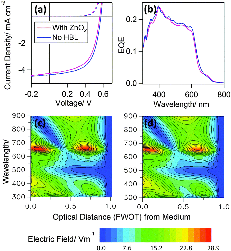 | ||
| Fig. 4 Performance characteristics of OPV devices with the structure: Al (70 nm)|Cu (8 nm)|Al (0.8 nm)|ZnOx (5 nm)|P3HT:PC60BM|MoO3 (5 nm)|Ag (11 nm) with and without a ZnOx HBL: (a) JV characteristics in the dark (dashed line) and under 1 Sun illumination (continuous line). (b) Corresponding EQE spectra. Models of the optical field distribution in the device with (c) and without (d) a ZnOx HBL performed using The Essential Macleod, Thin Film Centre Inc. software simulation package. | ||
| J sc/mA cm−2 | V oc/V | FF | η/% | |
|---|---|---|---|---|
| ZnO (5 nm) | 4.08 (±0.17) | 0.56 (±0.01) | 0.59 (±0.01) | 1.35 (±0.06) |
| No HBL | 4.05 (±0.17) | 0.57 (±0.002) | 0.61 (±0.01) | 1.42 (±0.05) |
Conclusions
In summary, we have shown that in the context of top-illuminated BHJ-OPVs for which the reflective substrate electrode extracts electrons, an electron selective interfacial layer is not required provided the work function of the electron-extracting electrode is less than the energy of LUMO of the donor material. The latter requirement is easily met using high performance narrow band gap electron donor polymers because these materials are characterised by a narrow band gap and relatively large ionisation potential, which results in a low lying LUMO energy. Through a study of the energetics at the interface between five widely used solution processed organic semiconductors (both donor an acceptor type) and a stable low work function reflective substrate electrode, we have shown that this electron selective/hole-blocking mechanism results from spontaneous ground state electron transfer from the electrode to both components of the BHJ giving rise to a Schottky-type junction. Removing this additional layer simplifies the fabrication of this important class of OPVs and so will help to maximise the cost advantage over other types of PV technology.Acknowledgements
This work was supported by the UK Engineering and Physical Science Research Council (EPSRC) (EP/K503204/1, EP/N009096/1 and EP/J500586/1) and European Regional Development Agency/Advantage West Midlands Science City Materials Initiative (Project 2). All data supporting this study are provided as supplementary information accompanying this paper. We also thank Professor Tim S. Jones for use of his group atomic force microscope.References
- C. J. Mulligan, M. Wilson, G. Bryant, B. Vaughan, X. Zhou, W. J. Belcher and P. C. Dastoor, Sol. Energy Mater. Sol. Cells, 2014, 120, 9–17 CrossRef CAS.
- L.-M. Chen, Z. Xu, Z. Hong and Y. Yang, J. Mater. Chem., 2010, 20, 2575–2598 RSC.
- H.-L. Yip and A. K.-Y. Jen, Energy Environ. Sci., 2012, 5, 5994–6011 CAS.
- L. K. Jagadamma, M. Abdelsamie, A. El Labban, E. Aresu, G. O. Ngongang Ndjawa, D. H. Anjum, D. Cha, P. M. Beaujuge and A. Amassian, J. Mater. Chem. A, 2014, 2, 13321–13331 CAS.
- Y. Chen, Z. Hu, Z. Zhong, W. Shi, J. Peng, J. Wang and Y. Cao, J. Phys. Chem. C, 2014, 118, 21819–21825 CAS.
- G. Kim, J. Kong, J. Kim, H. Kang, H. Back, H. Kim and K. Lee, Adv. Energy Mater., 2015, 5, 1401298 Search PubMed.
- A. Hadipour, R. Müller and P. Heremans, Org. Electron., 2013, 14, 2379–2386 CrossRef CAS.
- V. Kumar and H. Wang, Sol. Energy Mater. Sol. Cells, 2013, 113, 179–185 CrossRef CAS.
- S. Chambon, L. Derue, M. Lahaye, B. Pavageau, L. Hirsch and G. Wantz, Materials, 2012, 5, 2521–2536 CrossRef CAS.
- G. Long, X. Wan, B. Kan, Z. Hu, X. Yang, Y. Zhang, M. Zhang, H. Wu, F. Huang, S. Su, Y. Cao and Y. Chen, ChemSusChem, 2014, 7, 2358–2364 CrossRef CAS PubMed.
- A. Hadipour, D. Cheyns, P. Heremans and B. P. Rand, Adv. Energy Mater., 2011, 1, 930–935 CrossRef CAS.
- P. Peumans and S. R. Forrest, Appl. Phys. Lett., 2001, 79, 126–128 CrossRef CAS.
- Y. Zhou, T. M. Khan, J.-C. Liu, C. Fuentes-Hernandez, J. W. Shim, E. Najafabadi, J. P. Youngblood, R. J. Moon and B. Kippelen, Org. Electron., 2014, 15, 661–666 CrossRef CAS.
- J. Ham, W. J. Dong, J. Y. Park, C. J. Yoo, I. Lee and J.-L. Lee, Adv. Mater., 2015, 27, 4027–4033 CrossRef CAS PubMed.
- M. C. Barr, R. M. Howden, R. R. Lunt, V. Bulovic and K. K. Gleason, Adv. Energy Mater., 2012, 2, 1404–1409 CrossRef CAS.
- S. K. Hau, H.-L. Yip, N. S. Baek, J. Zou, K. O'Malley and A. K.-Y. Jen, Appl. Phys. Lett., 2008, 92, 253301 CrossRef.
- H.-W. Lin, S.-W. Chiu, L.-Y. Lin, Z.-Y. Hung, Y.-H. Chen, F. Lin and K.-T. Wong, Adv. Mater., 2012, 24, 2269–2272 CrossRef CAS PubMed.
- (a) Q. Bao, S. Fabiano, M. Andersson, S. Braun, Z. Sun, X. Crispin, M. Berggren, X. Liu and M. Fahlman, Adv. Funct. Mater., 2016, 1077–1084 CrossRef CAS; (b) R. M. Cook, L.-J. Pegg, S. L. Kinnear, O. S. Hutter, R. J. H. Morris and R. A. Hatton, Adv. Energy Mater., 2011, 1, 440–447 CrossRef CAS; (c) C. Tengstedt, W. Osikowicz, W. R. Salaneck, I. D. Parker, C.-H. Hsu and M. Fahlman, Appl. Phys. Lett., 2006, 88, 053502 CrossRef.
- N. Hayashi, H. Ishii, Y. Ouchi and K. Seki, J. Appl. Phys., 2002, 92, 3784 CrossRef CAS.
- H. Ishii, K. Sugiyama, E. Ito and K. Seki, Adv. Mater., 1999, 11, 605–625 CrossRef CAS.
- M. S. Tyler, O. S. Hutter, D. M. Walker and D. R. a. Hatton, ChemPhysChem, 2015, 16, 1203–1209 CrossRef CAS PubMed.
- B. Pradhan, S. Albrecht, B. Stiller and D. Neher, Appl. Phys. A: Mater. Sci. Process., 2014, 115, 365–369 CrossRef CAS.
- B. W. D'Andrade, S. Datta, S. R. Forrest, P. Djurovich, E. Polikarpov and M. E. Thompson, Org. Electron. Physics, Mater. Appl., 2005, 6, 11–20 Search PubMed.
- P. I. Djurovich, E. I. Mayo, S. R. Forrest and M. E. Thompson, Org. Electron. Physics, Mater. Appl., 2009, 10, 515–520 CAS.
- L. Kronik and S. Yoram, Surf. Sci. Rep., 1999, 37, 1–206 CrossRef CAS.
- R. J. Davis, M. T. Lloyd, S. R. Ferreira, M. J. Bruzek, S. E. Watkins, L. Lindell, P. Sehati, M. Fahlman, J. E. Anthony and J. W. P. Hsu, J. Mater. Chem., 2011, 21, 1721–1729 RSC.
- H. Ishii, N. Hayashi, E. Ito, Y. Washizu, K. Sugi, Y. Kimura, M. Niwano, Y. Ouchi and K. Seki, Phys. Status Solidi C, 2004, 201, 1075–1094 CrossRef CAS.
- S. R. Day, R. A. Hatton, M. A. Chesters and M. R. Willis, Thin Solid Films, 2002, 410, 159–166 CrossRef CAS.
- H. Ishii, H. Oji, E. Ito, N. Hayashi, D. Yoshimura and K. Seki, J. Lumin., 2000, 87–89, 61–65 CrossRef CAS.
- R. M. Cook, L.-J. Pegg, S. L. Kinnear, O. S. Hutter, R. J. H. Morris and R. a. Hatton, Adv. Energy Mater., 2011, 1, 440–447 CrossRef CAS.
- M. Iwamoto, A. Fukuda and E. Itoh, J. Appl. Phys., 1994, 75, 1607 CrossRef CAS.
- Y. Tanaka, K. Kanai, Y. Ouchi and K. Seki, Org. Electron. Physics, Mater. Appl., 2009, 10, 990–993 CAS.
- H. Yanagi, T. Kuroda, K. B. Kim, Y. Toda, T. Kamiya and H. Hosono, J. Mater. Chem., 2012, 22, 4278–4281 RSC.
- Y. Liang, Z. Xu, J. Xia, S. T. Tsai, Y. Wu, G. Li, C. Ray and L. Yu, Adv. Mater., 2010, 22, 135–138 CrossRef PubMed.
- P. Cheng, Y. Li and X. Zhan, Energy Environ. Sci., 2014, 7, 2005–2011 CAS.
- H. Yi, S. Al-Faifi, A. Iraqi, D. C. Watters, J. Kingsley and D. G. Lidzey, J. Mater. Chem., 2011, 21, 13649–13656 RSC.
- S. Wakim, S. Beaupré, N. Blouin, B.-R. Aich, S. Rodman, R. Gaudiana, Y. Tao and M. Leclerc, J. Mater. Chem., 2009, 19, 5351–5358 RSC.
- H. T. Nicolai, M. Kuik, G. a. H. Wetzelaer, B. de Boer, C. Campbell, C. Risko, J. L. Brédas and P. W. M. Blom, Nat. Mater., 2012, 11, 882–887 CrossRef CAS PubMed.
- Y. M. Yang, W. Chen, L. Dou, W. Chang, H. Duan and B. Bob, Nat. Photonics, 2015, 9, 190–198 CrossRef CAS.
- B. Ebenhoch, S. A. J. Thomson, K. Genevičius, G. Juška and I. D. W. Samuel, Org. Electron., 2015, 22, 62–68 CrossRef CAS.
- S. Zhang, L. Ye, W. Zhao, D. Liu, H. Yao and J. Hou, Macromolecules, 2014, 47, 4653–4659 CrossRef CAS.
- W. C. Tsoi, S. J. Spencer, L. Yang, A. M. Ballantyne, P. G. Nicholson, A. Turnbull, A. G. Shard, C. E. Murphy, D. D. C. Bradley, J. Nelson and J. S. Kim, Macromolecules, 2011, 44, 2944–2952 CrossRef CAS.
- M. C. Scharber, D. Mühlbacher, M. Koppe, P. Denk, C. Waldauf, A. J. Heeger and C. J. Brabec, Adv. Mater., 2006, 18, 789–794 CrossRef CAS.
- D. Chi, S. Qu, Z. Wang and J. Wang, J. Mater. Chem. C, 2014, 2, 4383–4387 RSC.
- J. Huang, G. Li and Y. Yang, Appl. Phys. Lett., 2005, 87, 112105 CrossRef.
Footnotes |
| † Electronic supplementary information (ESI) available. See DOI: 10.1039/c6mh00124f |
| ‡ Current address: London Centre for Nanotechnology and Department of Chemistry, University College London, 20 Gordon Street, London, WC1H 0AJ, UK. |
| § Current address: Diamond Light Source Ltd, Harwell Science and Innovation Campus, Didcot, Oxfordshire, OX11 0DE, UK. |
| This journal is © The Royal Society of Chemistry 2016 |