
 Open Access Article
 This Open Access Article is licensed under a
 Creative Commons Attribution 3.0 Unported Licence
CMOS biosensors for in vitro diagnosis – transducing mechanisms and applications
Ka-Meng
Lei
ab,
Pui-In
Mak
*ab,
Man-Kay
Law
a and
Rui P.
Martins
abc
aState-Key Laboratory of Analog and Mixed-Signal VLSI, University of Macau, China. E-mail: pimak@umac.mo
bFaculty of Science and Technology, Dept. of ECE, University of Macau, China
cOn leave from Instituto Superior Técnico, Universidade de Lisboa, Portugal
First published on 9th September 2016
Abstract
Complementary metal oxide semiconductor (CMOS) technology enables low-cost and large-scale integration of transistors and physical sensing materials on tiny chips (e.g., <1 cm2), seamlessly combining the two key functions of biosensors: transducing and signal processing. Recent CMOS biosensors unified different transducing mechanisms (impedance, fluorescence, and nuclear spin) and readout electronics have demonstrated competitive sensitivity for in vitro diagnosis, such as detection of DNA (down to 10 aM), protein (down to 10 fM), or bacteria/cells (single cell). Herein, we detail the recent advances in CMOS biosensors, centering on their key principles, requisites, and applications. Together, these may contribute to the advancement of our healthcare system, which should be decentralized by broadly utilizing point-of-care diagnostic tools.
I. Introduction
An essential part of evaluating the success of global health is the access to appropriate diagnostic tools.1 A commendable diagnostic tool should be able to rapidly identify disease occurring in individuals. Especially for infectious diseases, the turnaround time strongly affects their level of transmission to the community. In vitro diagnostic (IVD) tools aim to offer a comfortable experience for patients, by taking only a small specimen from the human body, e.g. blood, urine, sputum, and tissue. Consequently, technologies enabling effective in vitro diagnosis have become highly attractive in both developed and developing countries.2 Tremendous efforts have been geared towards clinical-level IVD tools. Despite achieving high accuracy, the result turnaround time can be too long for contagious diseases like Ebola and SARS, and the need for skillful operators to perform the assays can dramatically raise the cost.Recently, decentralized diagnostic solutions, namely point-of-care (PoC) devices, have gained notable interest, which is attributed to their rapidity, small footprint and tiny sample usage. A wide variety of diagnostic platforms have been invented, such as lateral flow assays3–6 and the path-breaking lab-on-a-disc7–10 for PoC applications. Beyond these, PoC devices on Complementary metal oxide semiconductor (CMOS) chips are particularly promising, as they can enjoy the maturity of microelectronics in manufacturing, and its outstanding performances in both physical sensing and signal processing. While the mainstream lateral flow assay is limited to providing merely qualitative or semi-quantitative results,11 CMOS biosensors can attain quantitative results and are beneficial to rapid and low-cost assays. Especially for low-cost IVD applications, CMOS chips on a centimeter scale can significantly miniaturize diagnostic tools.
Decentralized healthcare systems are highly attractive for developing countries, which typically suffer from lack of access to high-quality centralized diagnostic tools. Delays in diagnosis and treatment aggravate the healthcare condition of these countries, thus affecting the global health system. According to the World Development Report in 2004, lack of access results in failure of health services.12 Without proper equipment for diagnosis, diseases in resource-limited countries can only be diagnosed from their clinical symptoms. Yet, this may cause difficulties in diagnosing patients when their symptoms are still unobvious. Especially for infectious diseases, delays in treatment can worsen the situation of individuals, and consequently communities. According to a report by the World Health Organization (WHO), the leading infectious diseases (lower respiratory infections, HIV/AIDS, diarrhoeal diseases, malaria, and tuberculosis) account for roughly one-third of all deaths in low-income countries.13 Also, the strong growth in population in these areas gives rise to the demand for affordable IVD tools. By the end of 2050, the less-developed countries are expected to have a population of around 8.4 billion, as depicted in Fig. 1(a), where Africa and Asia contribute roughly 2.48 and 5.27 billion, respectively.14 Thus, there is a rapidly growing market for low-cost PoC devices for developing countries.
 | ||
| Fig. 1 (a) World population from 1950 to 2050, with a medium variant estimation from 2015. (b) The old-age dependency ratio (solid line), which is defined as the ratio of the population of 65+ year olds to the population of 15 to 64 year olds with a medium variant estimation from 2015. The child dependency ratio (dotted line), which is defined as the ratio of the population of 0 to 14 year olds to the population of 15 to 64 year olds, is also shown on the graph as reference. Data collected from the United Nations World Population Prospects: The 2015 Revision. More developed countries: Europe, Northern America, Australia/New Zealand, and Japan. Less developed countries: Africa, Asia (except Japan), Latin America, and the Caribbean, plus Melanesia, Micronesia and Polynesia. | ||
The aging problem of developed countries also creates an enormous challenge. A healthcare solution that can deal with the continuous increase in longevity is in demand. As revealed in Fig. 1(b), the old age dependency ratio, which gives an insight into the elderly population (65+ years) compared to those of working age (15 to 64 years), will be rising in the coming decades. Such an old-age dependency ratio in more developed countries will reach 0.4 in 2034, and eventually 0.46 by the end of 2050 (i.e., an increase of 72% from 2015). Thus, the burden on the clinical resources in those areas will become tighter, especially for the patients in close proximity to death.15 Thus, an efficacious healthcare system will benefit this situation, and drive the growth of the market for IVD tools. To this end, the market for IVD tools should not be merely aimed at less developed countries, but also towards efficient and convenient diagnosis in developed countries. In fact, according to a report from Forbes/Investing, the IVD market, valued at ∼$50 billion in 2012, will expand to ∼$70 billion by 2017.16 This paper studies and compares state-of-the-art CMOS biosensors tailored for in vitro diagnosis, including primarily the assay or monitoring of DNA, proteins, and cells. For the readout electronics of CMOS biosensors (e.g., amplifiers, filters, and oscillators), we refer readers to literature that emphasizes circuit-level challenges and realization.17,18 There are also review articles focusing on the system-level aspects of general PoC devices (not limited to CMOS), which discuss the design criteria and system requirements.2,19–27 Herein, we focus in detail on the transducing mechanisms of CMOS chips that could open up many possibilities for in vitro diagnosis.
After the introduction, different transducing mechanisms of CMOS PoC devices for biological sensing and targeting, namely electrical, magnetic, optical, mechanical, and nuclear spin, will be revealed. Then, different CMOS IVD tools for various targets of interest, such as DNA, protein and cells/bacteria will be discussed. Their pros and cons will be outlined and compared, offering the readers a systematic outlook on their distinct characteristics and limitations.
II. Transducing mechanisms of CMOS IVD tools
Rapid downscaling of CMOS technology has allowed the possibility of integrating billions of transistors onto a single chip, allowing ultra-fast signal processing at low power and cost. While their transformative effects on computers and mobile devices have been witnessed, the development of CMOS PoC devices for in vitro diagnosis only started recently. Along with circuit innovation, high-sensitivity analog interfaces are ready for CMOS biosensors. Thus, single-chip CMOS biosensors allow full integration of the transducers and circuits necessary for signal processing. This property aligns with the expectations for PoC devices, such as low sample consumption, small footprint, ease of use, and rapid and quantitative results. Attributed to the design flexibility of CMOS chips, multifarious CMOS biosensors have been reported, as listed in Table 1. Also, the capability to include post-processing steps (e.g., chemical deposition and micro-machining) after chip manufacturing can help in broadening the versatility of CMOS biosensors.28–33| Targets | Applications | Sensing parameters | Transducers | Labeling | Immobilization | Lowest amount reported | Year |
|---|---|---|---|---|---|---|---|
| DNA | DNA detection | Capacitance | Au electrodes | Label-free | Yes | N/A | 2006 (ref. 34) |
| DNA detection | Charge | ISFET | Label-free | Yes | 0.1 mM | 2006 (ref. 35) | |
| DNA detection | Magnetism | Spin-valve sensors | Magnetic particle (target) | Yes | 10 nM | 2007 (ref. 36) | |
| DNA polymerization | Charge | Polymer + metal | Label-free | Yes | N/A | 2008 (ref. 37) | |
| DNA detection | Fluorescence | Photodetector | Cy-3 label (target) | Yes | 0.125 nmol | 2009 (ref. 38) | |
| DNA detection | Fluorescence | Photodetector | Biotin and Qdot-655 (target) | Yes | 4 nM | 2009 (ref. 39) | |
| DNA detection | Magnetism | LC-oscillator | Digoxigenin & magnetic particle (target) | Yes | 1 nM | 2009 (ref. 40) | |
| DNA detection | Cyclic voltammetry | Au electrodes | Ferrocene redox label (target) | Yes | 4 nM | 2009 (ref. 41) | |
| DNA detection | Impedance | Au electrodes | Label-free | Yes | N/A | 2010 (ref. 42) | |
| DNA detection | Impedance | Au electrodes | Label-free | Yes | 5 μM | 2012 (ref. 43) | |
| DNA detection | Capacitance | Au electrodes | Label-free | Yes | 100 pM | 2012 (ref. 44) | |
| DNA detection | Charge | Au electrodes | Label-free | Yes | 100 pM | 2012 (ref. 45) | |
| DNA detection | Mass | Cantilever | Label-free | Yes | 1 pM | 2013 (ref. 46) | |
| DNA amplification & detection | Charge | ISFET | Label-free | No | 10 copies | 2013 (ref. 47) | |
| DNA detection | Charge | Silicon nanowire | Label-free | Yes | 3.2 pM | 2013 (ref. 48) | |
| DNA detection | Magnetism | LC-oscillator | Magnetic particle (probe) | Yes | 100 pM | 2014 (ref. 49) | |
| DNA detection | Cyclic voltammetry | Au electrodes | Label-free | Yes | 10 aM | 2014 (ref. 50) | |
| DNA amplification & detection | Fluorescence | SPAD | EvaGreen® dye | No | 1 copy | 2014 (ref. 51) | |
| DNA detection | Nuclear spin | Spiral coil | Magnetic particle (probe) | No | 50 pM | 2016 (ref. 52) | |
| Protein | C-reactive protein | Mass | Cantilever | Label-free | Yes | 1 μg mL−1 | 2009 (ref. 53) |
| Avidin | Nuclear spin | Spiral coil (off-chip) | Magnetic particle (probe) | No | 5 nM | 2009 (ref. 54) | |
| hMAM cancer marker | Mass | SAW transducer | Label-free | Yes | 1.5 μg mL−1 | 2010 (ref. 55) | |
| Protein G | Impedance | Au electrodes | Label-free | Yes | N/A | 2010 (ref. 42) | |
| hCG cancer marker | Nuclear spin | Spiral coil | Magnetic particle (probe) | No | 5 nM | 2011 (ref. 56) | |
| Human serum albumin | Magnetism | Hall sensor | Magnetic particle (probe) | Yes | 1 ng mL−1 | 2013 (ref. 57) | |
| SLPI cancer marker | Magnetism | GMR spin-valve sensor (off chip) | Magnetic particle (probe) | Yes | 10 fM | 2013 (ref. 58) | |
| Cardiac troponin I protein | Charge | Silicon nanowire | Label-free | Yes | 10 fM | 2013 (ref. 48) | |
| Cytokines (IL8, IFN, TNFα) | Chemiluminescence | Photodetector | Horseradish peroxidase | Yes | 3 pg mL−1 | 2014 (ref. 59) | |
| C-reactive protein | Capacitance | Au electrodes | Label-free | Yes | 0.5 mg L−1 | 2015 (ref. 60) | |
| Streptavidin | Fluorescence | Photodetector | Qdot 800 fluorophore | Yes | 48 zmol | 2015 (ref. 61) | |
| TNF-alpha & NT-probnp | Magnetism | Hall sensor | Magnetic particle (probe) | Yes | 0.8 pg mL−1 | 2015 (ref. 62) | |
| Multi-analyte | Chemiluminescence | Photodetector | Horseradish peroxidase | Yes | 45 ng mL−1 ferritin | 2015 (ref. 63) | |
| Human IgG | Nuclear spin | Spiral coil | Magnetic particle (probe) | No | 5 nM | 2016 (ref. 52) | |
| Mouse IgG | Magnetism | Microcoil (off-chip) | Magnetic particle (probe) | Yes | 100 pg mL−1 | 2016 (ref. 64) | |
| Cells/bacteria | Bovine aortic smooth muscle cell monitoring | Capacitance | Metal electrodes | Label-free | No | 20 × 20 μm2 | 2007 (ref. 65) |
| MDA-MB-231 breast cancer cell monitoring | Capacitance | Metal electrodes | Label-free | No | 20 × 20 μm2 | 2008 (ref. 66) | |
| Bladder cancer cell detection | Nuclear spin | Spiral coil | Magnetic particle (probe) | No | 17.5 cells per μL | 2011(ref. 56) | |
| MCF-7 breast cancer cell detection | Fluorescence | SPAD | 5D10 monoclonal antibody | No | Single cell | 2012 (ref. 67) | |
| MCF-7 breast cancer cell detection | Impedance | Au electrodes | Label-free | No | Single cell | 2012 (ref. 68) | |
| RBC flow cytometer | Impedance | Metal electrodes | Label-free | No | Single cell | 2012 (ref. 69) | |
| Cardiac progenitor cell monitoring | Magnetism | LC-oscillator | Magnetic particle (target) | No | N/A | 2012 (ref. 70) | |
| HeLa cell counting | Optics | CMOS image sensor | Label-free | No | 25 cells per mL | 2014 (ref. 71) | |
| Mouse embryonic fibroblast cell | Magnetism | Excitation & pickup coils | Magnetic particle (target) | No | Single cell | 2014 (ref. 72) | |
| Complete blood count | Optics | CMOS image sensor | Label-free | No | N/A | 2014 (ref. 73) | |
| HeLa cell counting | Cyclic voltammetry | Au electrodes | Label-free | No | N/A | 2015 (ref. 74) | |
| MCF7, BEAS, & K562 cancer cell monitoring | Capacitance | Au electrodes | Label-free | No | N/A | 2015 (ref. 75) | |
| Multiple cell monitoring | Multi-modal | Au electrodes & photodetector | Label-free | No | N/A | 2015 (ref. 76) | |
| HepG2 cancer cell monitoring | Optics | CMOS image sensor | Label-free | No | 5000 cells per mL | 2015 (ref. 77) |
According to their transducing mechanisms, CMOS PoC devices can be classified as: 1. electrical-based – directly sensing the electrical properties of samples, such as impedance or electric charges (currents); 2. optical-based – transducing the optical properties from the samples, such as fluorescence labels or chemiluminescence, into an electrical signal; 3. magnetic-based – transducing the magnetic properties of the samples arising from labeled magnetic particles (nano-particles) into an electrical signal; 4. mechanical-based – transducing the mechanical properties, namely the mass of the targets, to an electrical signal; 5. nuclear magnetic resonance (NMR)-based – transducing the nuclear spin from the sample, which is affected by the magnetic susceptibility, to an electrical signal. Details of each transducing mechanism and its corresponding example from Table 1 will be presented next.
Electrical-based
The capability of the CMOS chip to seamlessly handle electrical signals, such as current, impedance and capacitance, is ascribed to direct electronic detection biosensors, which are the most popular type of CMOS biosensors for in vitro diagnosis [Fig. 2(a)]. The electrical properties serve as a reliable measure to quantify the concentration of analyte inside the samples. The electrode acting as substrate for probe immobilization is usually formed by the top metal layer, which offers great feasibility for the downscaling of CMOS technologies, and is expandable to form an array for multi-targeting.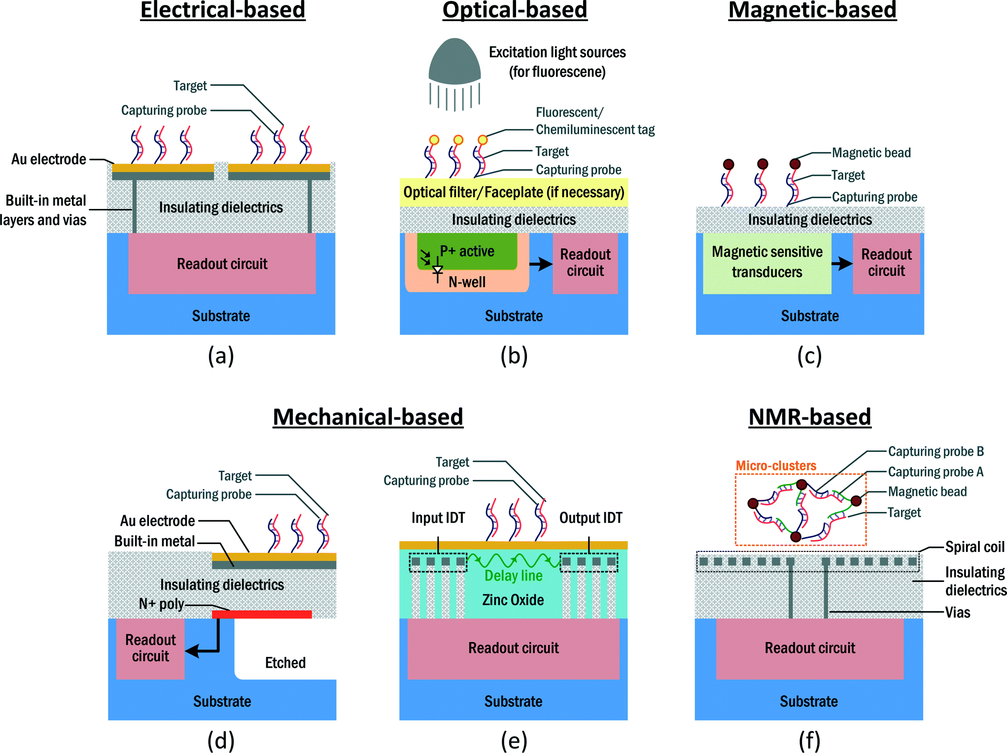 | ||
| Fig. 2 Architecture and operation of different CMOS biomolecule transducing mechanisms. (a) Electrical-based detection (excluding the FET-type biosensors). An extra layer of noble and biocompatible metal, such as gold, is deposited on the original built-in metal layer. The capturing probe is then immobilized on the gold electrode to capture the target. Upon hybridization, the electrical properties, such as impedance or charge, are sensed directly by the readout circuit. (b) Optical-based detection. The capturing probe is immobilized on a solid substrate, such as glass or the built-in passivation layer atop the CMOS chip. Then, a fluorescence-labeled or chemiluminescence-labeled target will bind with the probe and other unbound biomolecules will be washed away. The CMOS photodetector, which is formed by the embedded PN-junction, transduces the optical signal to current for subsequent signal processing. (c) Magnetic-based detection. The capturing probe is immobilized on a solid substrate, such as glass or the built-in passivation layer atop the CMOS chip. Then, the sample labeled with magnetic particles will mix with the capturing probe. The matched target will be captured and unbound objects will then be rinsed off. A magnetic transducer, such as an LC-oscillator or Hall sensor will transduce the magnetism of the sample to electrical signals, which will be subsequently processed by the readout circuit. (d) Mechanical-based detection with cantilever. A cantilever can be exploited to transduce the mass attached to it to electrical signals, such as resistance. A gold layer is deposited on the cantilever for growing the capturing probe on it. In order to allow the cantilever to bend upon attaching the biomolecule, the neighbouring insulating dielectrics and the base of the cantilever are etched away. A piezoresistor can be adopted to transduce the bending force on the cantilever to a resistance change, and the readout circuit will detect this variation. (e) Mechanical-based detection with SAW transducer. A complete SAW transducer consists of three modules, the input metal interdigital transducer (IDT), the piezoelectric delay line, which the acoustic wave travels through, and the output metal IDT. The input IDT generates the SAW. Then, the wave travels through the delay line to the output IDT, where the SAW is transduced back to the electrical signal. The bio-functionalized gold layer atop the delay line captures the entity under analysis. The increased mass here will affect the characteristics of the delay line, resulting in a change in resonant frequency, amplitude, or phase shift on the SAW, which can then be detected on the output IDT. (f) NMR-based detection. NMR focuses on the measurement of the NMR signals from the samples. First, the magnetic particle functionalized with the capture probes reacts with the sample under analysis. Then, the mixture will be placed atop the spiral sensing coil to perform the NMR experiment. The existence of a target inside the sample incurs particle aggregation, thus a larger micro-cluster will be formed, changing the spin–spin relaxation time of the NMR signal from the sample. | ||
A popular approach is electrochemical impedance spectroscopy (EIS), where the impedance between the electrodes is monitored over a range of frequencies. This provides details of the impedance changes of the solution and the electrode-solution interface. EIS has been involved in detecting affinity-based biosensing, which explores the binding events between the probe (i.e., complementary oligonucleotides, antibody/antigen) and the target within the samples. The probe can be immobilized on the electrodes with special chemical post-processing.78 Upon hybridization between the probe and target, the double-layer capacitance of the electrode-electrolyte interface decreases due to the increased thickness, together with the decreased dielectric constant, whereas the charge-transfer resistance increases, since the attached target partially blocks the flow of the ions.79 Thus, the system is capable of quantifying the analyte of interest by detecting the impedance between the electrodes. For instance, Manickam et al. showed a versatile EIS biosensor array on a CMOS chip.42 This fully integrated and label-free detecting platform is capable of quantifying different DNA and protein targets inside the samples with corresponding immobilized probes on the electrodes. Alternatively, the capacitance between the electrodes can also be used to detect the target upon the hybridization of DNA.80 Lee et al. reported a CMOS label-free capacitive biosensor for detecting DNA from the H5N1 virus.44 Instead of observing the complex impedance of the electrodes, this capacitive biosensor only focuses on the measurement of the capacitance of the electrodes, thus the circuit design can be simplified. The capacitive sensing mechanism is also an adequate candidate for cell monitoring. Prakash et al. presented a CMOS platform for cancer cell MDA-MB-231 proliferation monitoring [Fig. 3(a)].66 Since the capacitance can be sensed without removing the passivation layer, post-processing on the CMOS chip can be obviated [Fig. 3(b)]. The underlying principle is the insulating nature of the cell, together with the counterionic polarization in the surrounding aqueous medium on exposure to low-frequency electric fields, which accounts for the capacitive behavior of the cell [Fig. 3(c)].
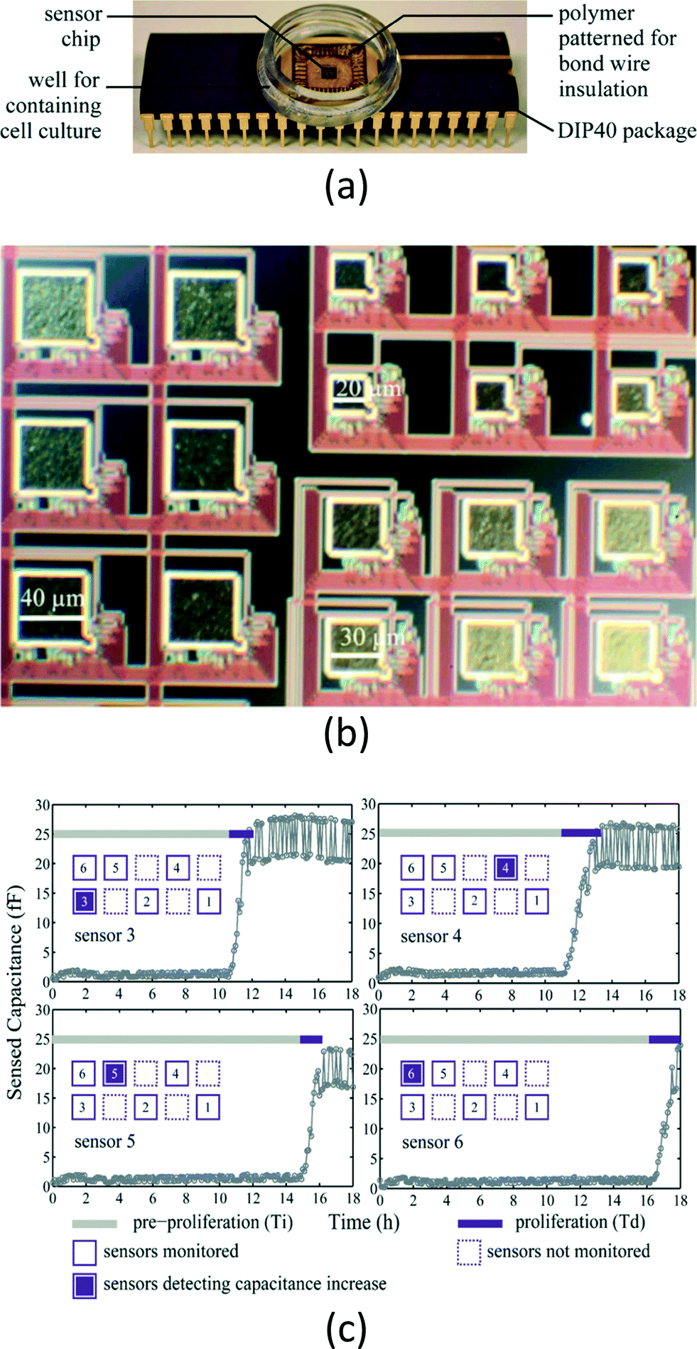 | ||
| Fig. 3 Cell culturing and monitoring with CMOS capacitive sensing chip. (a) A photograph showing the overall chip with dual in-line package. A well encloses the cell culturing site and the CMOS chip is in the center of the well. The bond wires of the chip are protected by the polymer. (b) Photomicrograph of the electrode. Since the system measures only the capacitance of the single electrode, the built-in passivation layer, such as silicon nitride and silicon dioxide, can be preserved without further post-processing. This simplifies the hardware preparation steps for biosensing. (c) The experimental results for cancer cell MDA-MB-231 culturing. The capacitance at a specific site increases due to the proliferation of the cancer cells, ascribed to the increased number of cells, allowing real-time monitoring of the growth of the cancer cells. Reproduced with permission from ref. 66. Copyright 2008 Elsevier. | ||
Alternatively, voltammetric, amperometric and potentio-metric techniques monitor the electrochemical reactions (i.e., charge transfer) within the samples directly. These electrochemical reactions are related to the concentration of the analytes. With a specific readout circuit, such as a potentiostat, these electrochemical reactions can be measured and the concentration of the biomolecule can be quantified. Levine et al. described a CMOS multiplexed electrochemical microsystem with a 4 × 4 electrode array for DNA detection.41 By sweeping the voltage between the electrodes, the current produced by a redox label on the target DNA sequence can be recorded by the on-chip electronics.
With the advance of post-processing in standard CMOS chips, special field-effect transistor (FET) biosensors, which sense the charges of ions/electrons from the target, such as ion sensitive FETs (ISFETs)35 and silicon nanowire (NW),33,48 also show promise for biomolecule detection. Compared to the standard electrical-based biosensors shown in Fig. 2(a), these have a different architecture and usually require further post-processing. Their operations are similar to MOSFET: the target concentration alters the charges on the surface of the FET, thus the physical properties of the channel are altered. For instance, Huang et al. reported a CMOS wireless biomolecular sensing system based on polysilicon NW.48 The resistance of the n-type doped polysilicon NW decreases upon the hybridization of complementary DNA on the NW, since the electrons in the NW are repelled from the surface. Thus, by detecting the resistance of the NW, the quantity of DNA inside the samples can be identified.
Optical-based
As the dominant detection modality for existing diagnostic tools is within the visible range of fluorescence spectroscopy, optical sensing still plays an important role in CMOS biosensing platforms, since conventional immunoassay protocols, such as ELISA, can migrate to the CMOS chip. The principle of fluorescent biomolecule assay is the detection of a fluorescence signal from a labeled fluorescent tag after washing the unconjugated tag. Upon excitation from an external light source, these fluorescent labels emit a signal at a longer wavelength due to Stokes shifting. Then, the designated transducer, such as a photodetector, which is implemented by an embedded PN-junction available in the standard CMOS process, can collect these signals and transduce them to the electrical domain (i.e., voltage or current) for signal amplification and conditioning [Fig. 2(b)].In order to integrate the fluorescence module into a CMOS chip, several considerations have to be taken into account. Firstly, since the signals are in the optical domain, the metal layers above the photodetector should be avoided to prevent blocking the signal. Secondly, as the intensity of the excitation signal is usually much stronger than the fluorescent signal, its presence at the photodetector will saturate it, thus causing system malfunctioning. Jang et al. proposed a CMOS fluorescence-based biosensor microarray for DNA detection.38 To filter the excitation signal and prevent it from reaching the photodetector, a separate 20 layer thin-film long-pass optical filter has to be put atop the CMOS chip. This filter rejects the excitation signal at 532 nm by 98 dB, while preserving a low passband attenuation of 1 dB. Furthermore, to direct the fluorescence signals with the photodetector, a fiber-optical faceplate was fabricated to guide the signals along the vertical direction. These CMOS-incompatible modules restrict the integration and raise the system cost. To this end, Huang et al. proposed an integrated time-resolved fluorescence detection CMOS array sensor suitable for DNA detection.39 Instead of removing the excitation signal by an optical filter, the proposed system adopts a time-gated arrangement to monitor the fluorescent decay of the labels after excitation. This scheme leads to a high signal-to-background ratio without any external filters. Lately, a fully integrated CMOS fluorescence biosensor with an on-chip nanophotonic filter was proposed.61 The design included an integrated optical filter obtained with back-end-of-line copper layers. This filter can suppress the excitation light without any external filtering/collimation, facilitating the integration of the entailed CMOS electronics and optical filters for fluorescent assays.
Similar to fluorescent detection, the chemiluminescent signal can also be detected from the signaling tag with a photodetector. The chemiluminescent tag, which emits a light signal based on the chemical reaction, averts the external light source to excite them. This prevents the saturation of the photodiode. Furthermore, the avoidance of an optical filter shortens the distance from the signaling tag to the surface of the photodetector, which fulfills the criteria for supercritical angle luminescence (SAL) and enables efficient signal detection.81 Sandeau et al. proposed a large-area CMOS bio-pixel array for multiplex biosensing.59 The high refraction index of the silicon substrate enables the SAL phenomenon and thus the direction of light emission from the chemiluminescent tag is confined to the surface, and the sensitivity is boosted by 100 fold compared to the standard microplate reader.
For larger biological objects, such as cells and bacteria, direct optical detection without a labeling tag is also feasible by using a high-speed CMOS image sensor. With the advance of CMOS imaging technologies, real-time cell monitoring and counting can also be achieved on a CMOS chip directly. The appearance of the objects blocks the photon from arriving at the CMOS image sensor, thus the system can count and monitor the activity of the cells/bacteria. Different cell monitoring systems based on CMOSs have been described in the literature. Saeki et al. proposed a lens-free cell counting device for HeLa cells with a microcavity array71 [Fig. 4(a) and (b)]. The cells are trapped on the microcavity array by applying a negative pressure underneath. Hence, the cells trapped inside the microcavity block the light from the light emitting diode and create a shadow on the CMOS image sensor, thus the CMOS image sensor can enumerate the cells on the array [Fig. 4(c) and (d)].
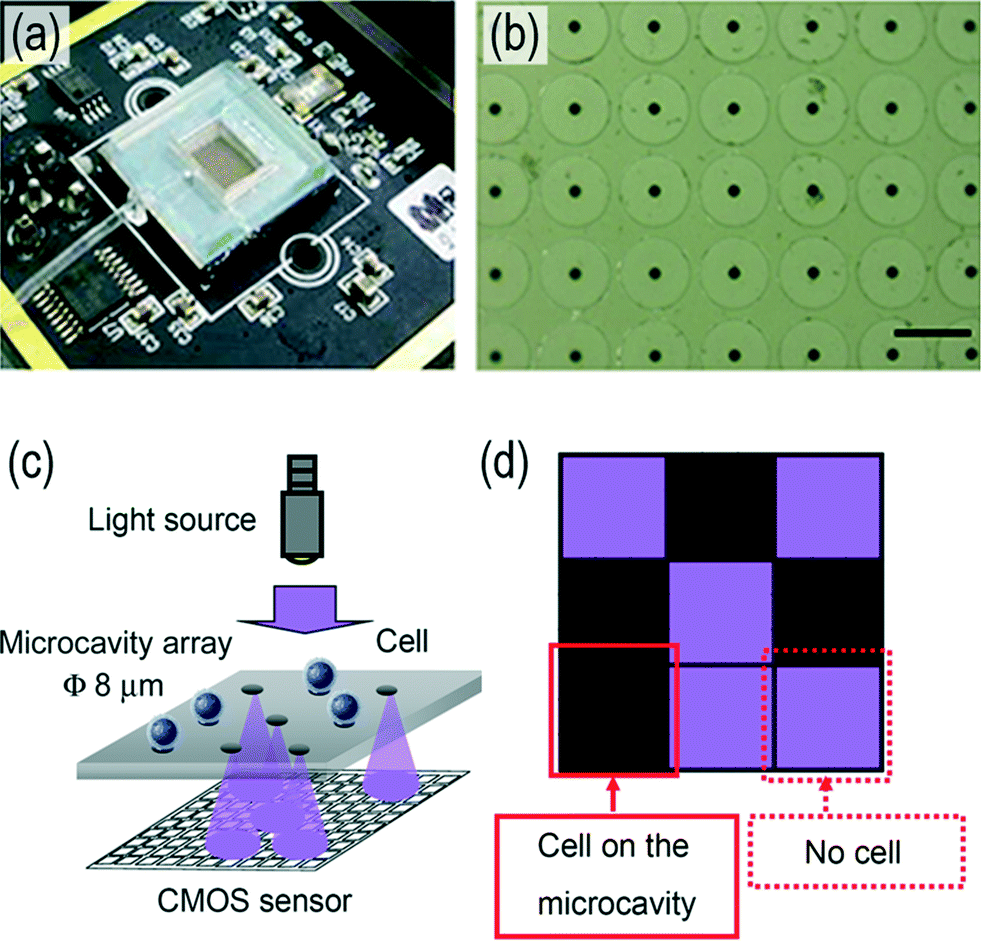 | ||
| Fig. 4 Lens-free cell/micro-particle counting system with CMOS image sensor. (a) The overall platform of the digital cell counting device. (b) A micrograph of the microcavity array for cell trapping. The sample under analysis is put atop the micro-cavity array. Then, the suspended cells/micro-particles will be pulled toward and trapped in the cavities by the negative pressure. This negative pressure is produced by a peristaltic pump, which extracts the air inside the chamber. (c) Detection principle of the system. The light from the external UV light source will arrive at the CMOS image sensor through the unoccupied cavity, while the trapped cell on the cavity blocks the light from arriving at the CMOS image sensor. (d) The schematics of the expected CMOS image acquired from (c). Since the cell blocks the UV light from passing through the cavity, the pixels under the occupied cavity will report a darker region, while the pixels under the vacant cavity will report a brighter result. Thus, the number of cells on the microcavity array can be identified from the result from the CMOS image sensor. Reproduced with permission from ref. 71. Copyright 2014 Saeki et al. | ||
Magnetic-based
Magnetism has recently become a tantalizing mechanism for biomolecule detection. Ascribed to the absence of magnetic signal in the sample and background, magnetism originating from the labeled magnetic micro- or nano-particles can be clearly detected from the samples. In addition, as the magnetic field can penetrate the insulating dielectric layers, direct contact between the samples and the transducers is avoided. This simplifies the hardware preparation of the CMOS chip before the assay. The basic operation is to grow an immobilization layer on a surface proximal to the transducer, similar to the electrical- and optical-based biosensors. Then, the magnetic-labeled sample can be placed on the transducer for hybridization. After a washing step to flush the unbound biomolecules and magnetic particles, the target of interest with magnetic particles will stay on the surface, allowing the transducer to detect the corresponding signal if the target exists inside the sample [Fig. 2(c)].There are diverse transducers to convert this magnetism to an electrical signal. For instance, a Hall sensor can be adopted to sense the magnetic field and transduce it to voltage/current signals. The Hall sensor, composed of n-type silicon, can offer moderate mobility (i.e., sensitivity) yet be fully compatible with the CMOS process. The current carriers in the sensor experience a Lorentz force when there is a magnetic field orthogonal to the direction of current flow applied to them. This causes charge deflection and allows electronic detection. Gambini et al. proposed a CMOS Hall sensor array for immunoassays.57 A Hall sensor was adopted to perform the relaxation measurement on the magnetic field and transduce this to a voltage signal. With the bound magnetic particles, the relaxation of the magnetic field from the particles relaxes to zero, according to the Néel relaxation mechanism. Thus, by detecting this relaxation time, the concentration of the magnetic particles (i.e., the target concentration) can be detected. Alternatively, an inductor can also be employed to sense the magnetism of the samples. As the inductance is heavily affected by the proximal magnetic susceptibility, the target can be quantified by detecting its inductance. Pai et al. presented a CMOS magnetic biosensor array for DNA and protein detection using an embedded LC-oscillator (L and C represent the inductor and capacitor), where the inductor implementation uses the top metal layer of the CMOS chip [Fig. 5(a)–(c)].49 The bound magnetic particles are detected from the oscillation frequency of the oscillator. They demonstrated the detection of DNA with a concentration of 100 pM by a novel magnetic freezing technique to reduce the sensor noise [Fig. 5(d)].
 | ||
| Fig. 5 magnetic-based handheld diagnostic device for antigen and nucleic acid detection. (a) The overall platform of the diagnostic device. The CMOS chip is easily plugged in on the print circuit board with a cartridge. (b) The disposable cartridge with the CMOS chip. The CMOS chip is attached to the cartridge with silver epoxy and connected with bond wire to the carrier leads. This arrangement enables a disposable, low-cost and multiplexed assay, and simplifies the sample handling module, such as microfluidic, to manage the sample to the sensing sites. (c) The CMOS chip. It has 48 on-chip sensing sites, together with 16 reference sensors. Each coil, together with its own capacitor, forms an LC-oscillator, which has an oscillating frequency inversely proportional to the square root of the inductance of the coil. The surface of the chip is biofunctionalized for probe immobilization. The sample with the magnetic particle is then applied on the surface of the chip, followed by a washing step to rinse the unbound molecules and magnetic particles. The bound magnetic particles increase the inductance of the coils, thus by detecting the oscillation frequency, the concentration of the target at a specific site can be selectively evaluated. (d) The experimental results for DNA detection. The frequency shift of the oscillation frequency is commensurate with the concentration of the target. With the novel magnetic freezing scheme, a limit-of-detection of 100 pM DNA can be achieved. Reproduced with permission from ref. 49. Copyright 2014 RSC Publishing. | ||
Mechanical-based
Mass is a fundamental parameter for analyzing the concentration of a target by utilizing an immobilized probe on the transducer without a labeling process. The probes capture the targets in the samples and thus the mass on the transducer increases. Then, a specific transducer converts the mass variation to an electronic signal.An example of this kind of mechanical transducer is the cantilever [Fig. 2(d)]. This senses the concentration of the analyte by the mass attached to the cantilever, and it is designed to work in a static or dynamic mode.82 In the static mode, only one surface of the cantilever is bio-functionalized and thus bending occurs statically in one direction. While working in the dynamic mode, the entire cantilever operates in the capture of the targets, with its resonant frequency sensitive to the mass attached. By adopting a special design and post-processing, such as etching and additional layer depositing, the CMOS chip is capable of embodying a cantilever and transduces the mass attached to electrical signals. If the targets are presented in the samples, the probe will seize the targets, raising the mass of the cantilever as a mechanical effect. This event can be detected from the resistance, resonant frequency, or optical deflection of the cantilever, depending on the design and criteria of the platforms. Chen et al. demonstrated a silicon-based micro-cantilever to detect C-reactive protein from a sample.53 The deflection ascribed to the additional mass on the cantilever is detected by the displacement of an optical beam, which is reflected by the surface of the cantilever and detected by another photodetector chip. Yet, the separate modules and the inclusion of the optical gadgets (i.e., laser beam generator, lens and mirror) restrict the integration of the systems, and reduce their applicability outside the laboratory. Subsequently, an integrated cantilever system-on-chip for label-free DNA hepatitis B virus detection was proposed by the same group.46 In this work, the deflection of the cantilever is detected by an embedded n+ polysilicon piezoresistor, whose resistance varies depending upon the bending of the cantilever [Fig. 6(a) and (b)]. Hence, the optical gadgets can be eliminated, allowing the integration of the cantilever with the readout circuitry. They demonstrated the detection of DNA from the hepatitis B virus after washing and drying of water molecules from the cantilever, with a sensitivity as low as 1 pM [Fig. 6(c)].
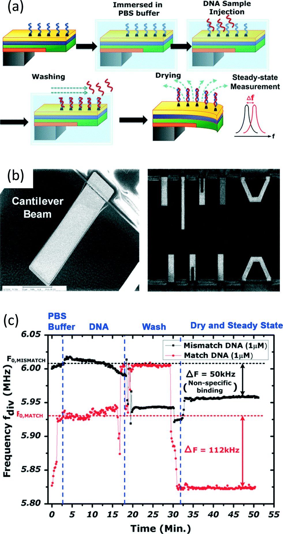 | ||
| Fig. 6 A CMOS cantilever-based biosensor for DNA detection. (a) The operation procedures of the biosensor. After post-processing to implement the cantilever on the CMOS chip, the captured DNA is immobilized on the Au surface of the cantilever. Then, the cantilever is immersed in the PBS buffer and the sample of interest is injected around the cantilever to allow hybridization of DNA. After washing off the unbound biomolecules, the cantilever is left to dry. After all of the water molecules are evaporated, the matched target DNA will stay on the Au surface. Their masses incur bending of the cantilever and an embedded piezoresistor implemented by N+ polysilicon is entailed to sense this bending, and transduce it to variation of its own resistance, causing a frequency shift on the ring-type oscillator. (b) An SEM image showing the cantilevers. In order to allow the cantilever to bend freely in air, the surrounding materials, such as the insulating dielectrics and p-substrate underneath, have to be etched away, creating a suspended cantilever. (c) Experimental results for the biosensor. The resistance variation of the polysilicon piezoresistor, attributed to the bending of the cantilever, incurs a deviation of the oscillating frequency. After DNA sample injection, and washing and drying steps, the final steady-state frequency can be measured to selectively quantify the concentration of the target DNA inside the sample, with a limit-of-detection of 1 pM, from the hepatitis B virus. Reproduced with permission from ref. 46. Copyright 2013 IEEE. | ||
Another novel type of mechanical transducer in CMOSs is the surface acoustic wave (SAW) transducer [Fig. 2(e)], which detects the acoustic wave transmission pattern between two transducers. When the target binds with the immobilized probe in the acoustic wave transmission path (delay line), the properties of the output will change, thus allowing mass detection.83 Tigli et al. proposed a SAW biosensor in CMOS technology to detect the cancer marker, human mammaglobin (hMAM).55 By adopting a post-processing step, a piezoelectric zinc oxide layer can be deposited on the CMOS chip. This zinc oxide layer affects the resonant frequency of the SAW along the delay line, according to the mass attached to it, permitting the quantification of the hMAM biomarker.
NMR-based
Recently, nuclear magnetic resonance (NMR) has gained popularity for biomolecule detection. The underlying physics of NMR is the exchange of energy between the nuclear spins of the nuclei and the radio-frequency magnetic field in the presence of a static magnetic field. Similar to the magnetic sensing scheme, NMR-based biosensors rely on magnetic labels to selectively detect the target. Yet, they indirectly detect these magnetic labels from the 1H NMR signals of aqueous samples. The spin–spin relaxation time of the NMR signals will be disturbed by the magnetization and the size of the magnetic nanoparticles.84 The probe-decorated magnetic nanoparticles stay mono-dispersed before mixing with the target. After mixing with the target inside the samples, the probe binds with the target and thus the magnetic nanoparticles gather and form micro-clusters. These micro-clusters have a larger size and different magnetization, and thus the relaxation time of the sample will change accordingly. By detecting the NMR signals from the samples, the concentration of the target can be quantified from their spin–spin relaxation time. A NMR spiral sensing coil implemented by a top metal layer transduces between the electrical signals from the readout circuit and the magnetic field generated by the nuclear spins [Fig. 2(f)]. Compared to the direct magnetic sensing scheme, the NMR-based technique radically eases the hardware preparation, since immobilization is not required.The versatility and flexibility of NMR-based biosensing enable different types of biomolecule assays. While NMR-based detection was originally performed with a discrete prototype,85–91 significant efforts have evolved to integrate the electronics and detecting coil into a single CMOS chip for portable and low-cost assays. For instance, Sun et al. reported a one-chip NMR system to detect protein, cancer markers and bladder cancer cells inside 5 μL samples,56 equipped with a transceiver along with the sensing coil to perform the NMR experiment and enable lab-on-a-chip operation. Also, we demonstrated an integrated NMR system with an on-chip sensing coil and magnetic field stabilization module [Fig. 7(a)].52 This stabilization module enhances the robustness of the platform against ambient variations, such as temperature. The functionality of the platform has been evinced by the detection of human immunoglobulin G and synthesized DNA from Enterococcus faecalis in 2.5 μL samples [Fig. 7(b) and (c)].
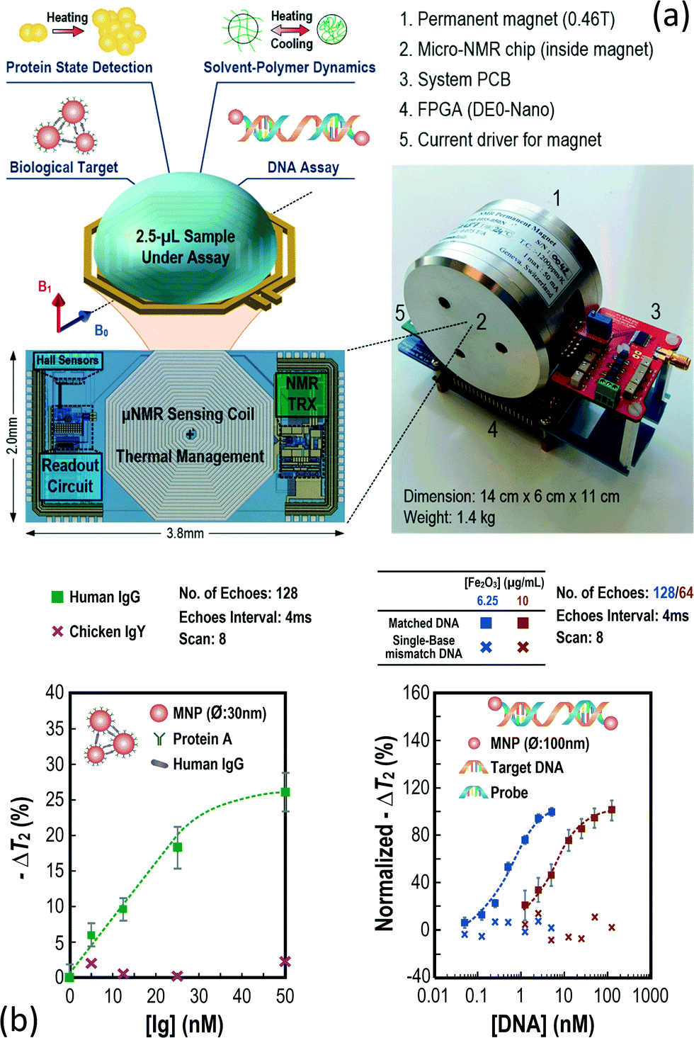 | ||
| Fig. 7 The handheld micro-NMR relaxometer for chemical or biological assays. (a) The proposed micro-NMR platform. This consists of five main modules: 1. portable magnet for magnetizing the protons from the samples. 2. A micro-NMR chip for performing the NMR experiment. 3. System PCB for biasing and powering the chip. 4. The field programmable gate array for controlling the hardware and also communicating with the host (computer). 5 current driver to inject the current to the auxiliary coil of the magnet to stabilize the magnet field and safeguard the operation. The CMOS chip comprises an NMR transceiver, NMR sensing coil and Hall sensor to sense the magnetic field variation from the magnet. The sample under assay is put atop the sensing coil for analysis. Benefitting from the versatility of the NMR experiment, different assays such as biomolecule targeting and protein state analysis can be performed on this platform, rendering it suitable for healthcare, the food industry and colloidal applications. (b) The biomolecule targeting results. The platform can selectively detect the concentration of the target by analyzing the spin–spin relaxation time from the detected NMR signals. By entailing different probes, the platform is capable of detecting different kinds of biomolecules, such as human immunoglobulin G and DNA derived from Enterococcus faecalis without post-processing on the CMOS chip. Reproduced with permission from ref. 52. Copyright 2016 IEEE. | ||
III. In vitro diagnostic applications
In vitro diagnosis focuses on analyzing targets from specimens. Different biological objects, such as protein, DNA or cell/bacteria, can be targeted. This section introduces assays with CMOS biosensors and their biological applications suitable for in vitro diagnosis, according to Table 1.Immunoassay
The prevailing assay for detecting protein-based targets is the enzyme immunoassay. It is based on an enzyme-labeled antibody (antigen) to detect the target antibody (antigen). The most dominating method of enzyme immunoassay is the enzyme-linked immunosorbent assay (ELISA).92 By observing a visual signal, such as a color change from an enzyme or fluorescent label, the concentration of a target inside a sample can be quantified. ELISA is referred as the golden standard in the clinical laboratory for a broad range of applications, such as dengue,93 cancer markers,94 and H5N1 influenza.95Despite the popularity of ELISA in conventional laboratories, ELISA is labor-intensive and time-consuming, limiting its prevalence in resource-limited areas (e.g., forest). In this regard, significant efforts have been focused on migrating the immunoassay to a CMOS chip for superior performance and small-form factor. Klapproth et al. demonstrated a multi-analyte CMOS sensor to measure multiple sandwich-ELISA reactions performed on the CMOS chip.63 The chemiluminescence is recorded by the on-chip photodetector working in the reverse-bias region. This allows parallel detection of different biological targets, such as immunoglobulin E and myoglobin, and shows comparable results to the clinical protocols. Alternatively, Kuo et al. reported a smart CMOS assay system-on-chip platform for rapid blood screening with a Hall sensor to transduce the magnetic field generated by an on-chip magnetic coil to a voltage signal62 [Fig. 8(a)]. An anodic aluminium oxide membrane filters the biomarkers from the blood sample. Then, the filtered sample is pumped to the Hall sensor array for immunoassay by the electrolytic electrodes [Fig. 8(b)]. With the bound magnetic particles, the magnetic field generated by the coil will be enhanced. The system is capable of detecting a biological target, such as tumor necrosis factor-α for anti-tumor response and N-terminal pro-brain natriuretic peptide for heart failure response, from whole blood [Fig. 8(c)].
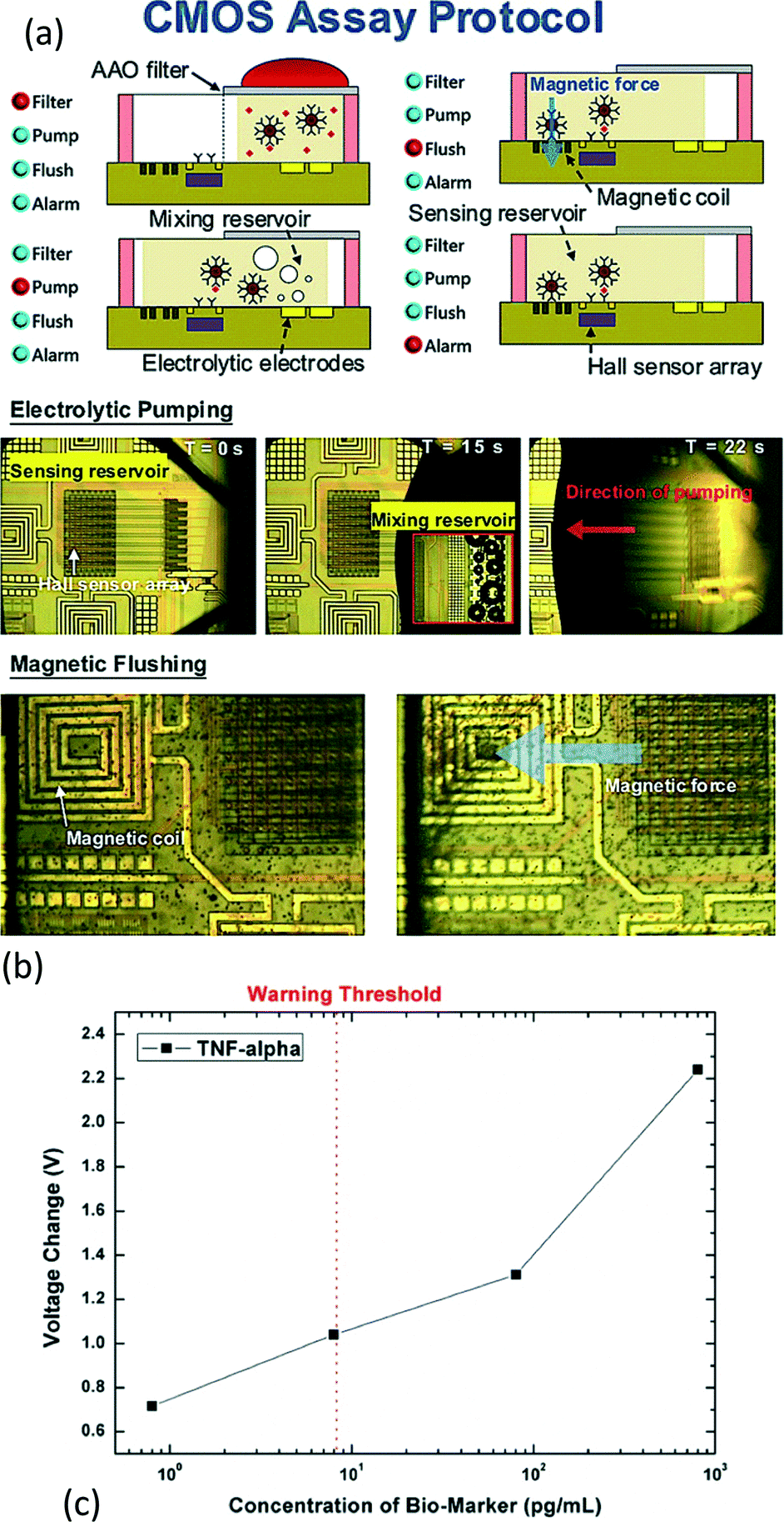 | ||
| Fig. 8 Smart CMOS system-on-chip platform for rapid blood screening test for risk prediction. (a) The experimental procedure of the platform. Firstly, the blood under analysis is put atop the anodic aluminium oxide membrane. The biomarkers will be diffused to the mixing reservoir and separated from other blood cells (>1 μm). After filtration, the filtered sample in the mixing reservoir, together with the bio-functionalized magnetic bead, will be pumped to the sensing site by the force from the electrolytic pumping. Upon capturing by the coated antibody at the surface of the CMOS chips, the target and the magnetic bead will be seized, while the unbound magnetic bead will be flushed away by the magnetic force from the on-chip coil. Thus, the Hall sensor can sense the magnetic bead and identify the concentration of the targeted biomarker. (b) A photograph showing the electrolytic pumping and magnetic flushing. At first, the sample is on the right of the sensing reservoir. Then, a voltage is applied on the electrolytic electrodes and bubbles are formed as a consequence. The bubbles here induce a gas force and pump the sample to the sensing reservoir. After the sample arrives at the sensing site, the immobilized antibodies capture the targets and the magnetics beads. Then, the unbound magnetic beads will be flushed away by the on-chip coil. (c) The experimental result (TNF-alpha) of the immunoassay. The Hall sensor detects the target analyte from the magnetic beads on the sensing site. The system can detect 0.8 pg mL−1 to 80 ng mL−1 of TNF-alpha and NT-proBNP from whole blood. Reproduced with permission from ref. 62. Copyright 2015 IEEE. | ||
DNA hybridization assay
Diagnosis with DNA biomolecules has a broad range of applications, such as mutation in DNA sequences for cancer prediction96 and pathogen detection. Detection of the specific DNA is grounded on DNA hybridization detection. DNA hybridization is a molecular biology technique used to identify a sequence of interest, which is analogous to immunoassay. A single strand DNA complementary to the target DNA acts as a probe and is used to selectively detect the target. If the target DNA is complementary to the designated probe, DNA hybridization occurs and double-stranded DNA will be formed. Then, the detector will detect the designated signaling tag to quantify the target DNA inside the sample.Conventionally, DNA detection relied on fluorescence-based detection similar to immunoassay.97 This shares similar drawbacks with the immunoassay, such as bulky optical instruments. Thus, considerable efforts have been geared towards implementing the DNA assay tool with a CMOS chip for multifarious biological purposes. For instance, Jafari et al. proposed a nanostructured CMOS ultra-wideband label-free PCR-free DNA detection system.50 This supports 54 channel fast-scan cyclic voltammetry DNA analysis. The electrical-based transducing mechanism here enables the complete integration of the platform, including the transducers (electrodes), current readout circuit, waveform generator for cyclic voltammetry, and transmitter for communication. The system demonstrated label-free detection of prostate cancer synthetic DNA without DNA amplification, featuring a detection range from 10 aM to 10 μM. In another study, Norian et al. implemented an integrated CMOS quantitative-polymerase-chain-reaction (qPCR) lab-on-chip platform by integrating a thermal module, a digital microfluidic module and a single-photon avalanche diode (SPAD) on a single CMOS chip [Fig. 9(a)].51 The proposed platform achieved fully integrated qPCR instrumentation, with proof-of-concept detection of DNA from Staphylococcus aureus with a detection limit down to 1 copy per 1.2 nL droplets, reducing the reagent consumption by 40![[thin space (1/6-em)]](https://www.rsc.org/images/entities/char_2009.gif) 000× [Fig. 9(b)].
000× [Fig. 9(b)].
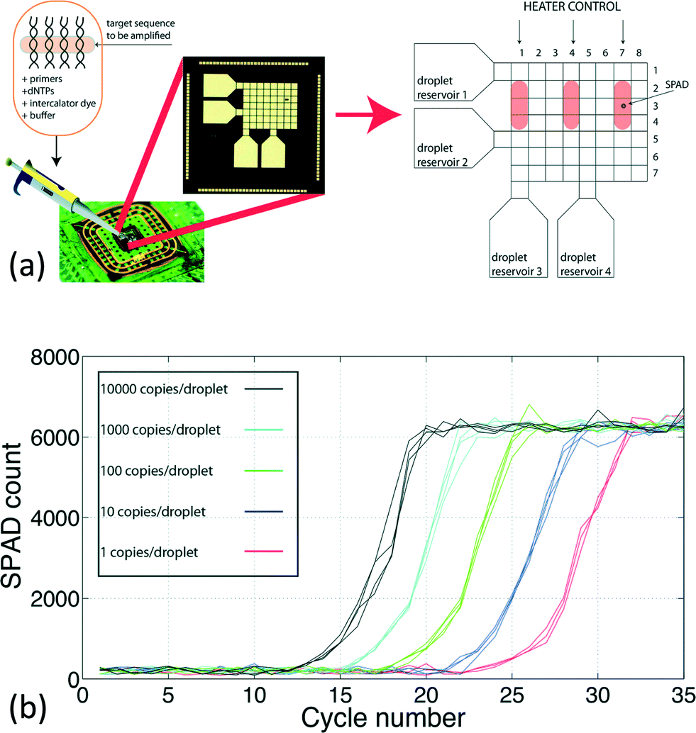 | ||
| Fig. 9 Integrated qPCR system on CMOS chip. (a) The CMOS chip and illustrations of its functions. The chip has three main modules to enable on-chip qPCR. An electrowetting-on-dielectric device serves as an electronic-automated droplet management module to extract the target, PCR reagents, buffer, and intercalator dye from the reservoirs, and guides them to different electrodes for mixing and subsequent operations by applying a voltage on corresponding electrodes. A thermal module, which is formed by a resistive heater and temperature sensor, regulates the temperature of the droplets to perform thermal cycling for a polymerase-chain-reaction. A single photon avalanche diode is embodied on the CMOS chip to detect the fluorescent emission from the target DNA in real-time for qPCR. (b) Experimental results of the qPCR. The fluorescent signal from the sample increases with the PCR cycle. The qPCR system achieves a linear relationship between the cycle threshold and logarithm of the initial DNA concentration from 1 to 10000 copies per 1.2 nL of droplets, resulting in a 40000 fold reduction of the reagent consumption. Reproduced with permission from ref. 51. Copyright 2014 RSC Publishing. | ||
Cell/bacteria diagnosis
Cell level diagnosis also plays a significant role in the IVD field. An example is the counting of CD4+ T cells in human whole blood to spot the human immunodeficiency virus (HIV) infection. CD4+ T cells are a type of white blood cell that is essential to the human immune system. Upon infection by the HIV virus, the CD4+ T cells are depleted and thus the immune system is degenerated. An efficient approach to diagnosing and monitoring HIV infection is CD4+ T cell counting. Flow cytometry is the golden standard for counting CD4+ T cells.98 The basic principle is to enumerate the CD4+ T cells passing through the detector during continuous flow of the sample. The appearance of the CD4+ T cells will alter the parameters of interest, such as impedance, or the light beam on the photodetector, such that the number of cells inside the samples can be counted. Yet, a conventional flow cytometer requires bulky detection tools and a large volume of sample. In this regard, Lee et al. proposed a CMOS impedance cytometer to monitor the flow inside the PDMS microchannel.69 They utilized the cytometer to diagnose the rigidity of the red blood cells (RBC). A rigid RBC opposes deformation caused by shear stress in the medium, and is related to distinctive diseases, which offers a potential for micro-circulation study.Another key application of cell-level diagnosis is cell monitoring for growth, cytotoxicity, and virus detection inside the cell. Monitoring the cellular activity (i.e., cell division, apoptosis, and necrosis) using electronics enables real-time automated assay on designated cells, when compared with the traditional microscopic approach. There have been efforts to monitor the cells using different electronic-based techniques, such as impedance sensing and imaging for different diagnostic purposes. For instance, Chi et al. proposed a CMOS 3 × 3 multi-modal cell-assay platform for cellular assay [Fig. 10(a) and (b)].76 Benefitting from the high integration level of the CMOS technology, different types of sensors, such as photodiodes, temperature sensors, and impedometers, are integrated within a single pixel, rendering it a promising platform for joint-modality cellular physiological monitoring. Various cells, such as ovarian cancer cells and human cardiomyocytes have been entailed for biological experiments and verification [Fig. 10(c)]. Recently, Laborde et al. reported a 256 × 256 nanocapacitor array for real-time imaging of microparticles and living cells on a CMOS chip.75 By simultaneously exploring the benefits of CMOS technologies, they achieved label-free and high-throughput monitoring of different cancer cells with attofarad resolution on the sub-micrometer scale.
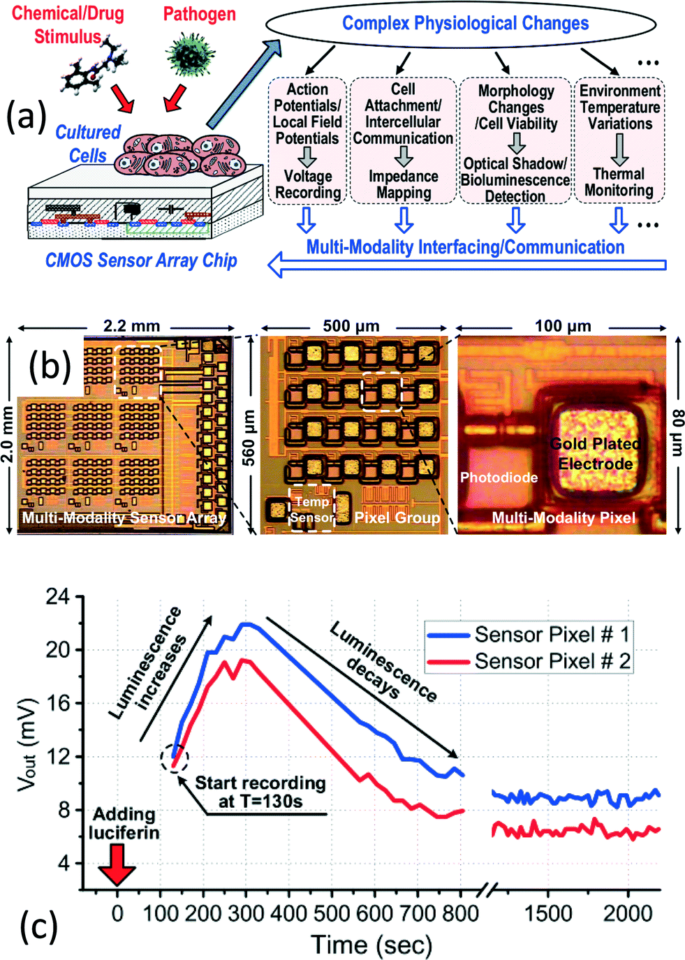 | ||
| Fig. 10 CMOS multi-modal sensor array for cell-based assay. (a) Schematic of the multi-modal cell-based assay platform. The entire platform consists of a 3 × 3 sensor array and each pixel consists of a photodiode, a temperature sensor (shared within a pixel group), a voltage amplifier, and an impedance detector for multi-modal study and monitoring of the cultured cells exposed to drug or pathogen stimulation. (b) A micrograph of the CMOS cellular sensor chip. The chip contains 9 pixel groups for individual cell-based assay and each pixel group further contains 16 individual pixels. Each pixel is formed by a gold plated electrode for action potential and impedance reading with a photodiode. (c) Real-time experimental results from the bioluminescence experiment at 2 pixels. The human ovarian cancer cell emits luminescence upon the addition of luciferin, enabling verification of cell viability. The photodiode captures this bioluminescence and the readout circuit processes the signal for subsequent analysis. Reproduced with permission from ref. 76. Copyright 2015 IEEE. | ||
IV. Discussion and selection guide
Since there is high diversification of the characteristics and properties of CMOSs in vitro biosensors, as shown in Table 1, we aim to summarize a selection guide and provide a radar chart of each transducing method. Herein, we analyze and discuss the properties, requisites, and limitations of CMOS biosensors, based on their transducing mechanisms, evaluated in terms of the integration level, labeling scheme, hardware preparation, operation steps, and specificity.Integration level
For cost and size minimization, the integration of all necessary hardware of the biosensor into a unified platform is desirable. Electrical-based detection is an ideal solution for sensing both small biomolecules (DNA and proteins) and large biological objects (cells and bacteria). External non-electronic gadgets (e.g., light sources, optical filters, or magnets) can be avoided. Similarly, mechanical-based detection is a promising method of biosensing, except for the case of utilizing a laser beam for detecting cantilever deflection.53 Traditionally, magnetic-based detection involves either a permanent magnet49 or external coil58 to magnetize and sense magnetic particles. Yet, there have been certain efforts to eliminate these external gadgets by implementing the coil-on-chip62 or adopting the LC-oscillator40 to sense magnetic particles. Optical-based biomolecule detection, especially for fluorescence, shares the same drawbacks as centralized benchtop assay, such as the need for excitation light sources. NMR-based detection, in this perspective, is difficult for integration since it involves a large permanent magnet (typical size of the magnet for NMR: 8 cm in diameter; 5.5 cm in height) for performing the NMR experiments. Furthermore, the magnetic field generated by the permanent magnet is temperature-dependent, and calibration is required to ensure proper operation.52,89Labeling
The labeling process determines the effort and difficulties associated with preparing the sample and corresponding probes. Label-free assay is preferable, as it does not require complicated signal tags, such as fluorescence, redox-active molecules, and magnetic particle labeling on the sample and probe to detect the target. Electrical and mechanical-based detection are superior in this area since they both support label-free detection. While certain studies entailed redox tagging for signaling,41 most of the electrical/mechanical-based biosensors are label-free, simplifying the sample preparation before the assay. On the other hand, NMR-based biosensors utilize magnetic particles functionalized with the capturing probe for detection. The labeling process restricts the experiments when compared with electrical/mechanical-based biosensors. Nevertheless, since surface functionalization only entails a probe, instead of a target, the sample under assay can remain unprocessed. Optical/magnetic-based biosensors involve attaching fluorescent, luminescent or magnetic labels on the target for assaying, which substantially increases the effort and cost of the assay. Yet, a sandwich-based bioassay technique can be applied to circumvent labeling the target to reduce the number of sample preparation steps.Hardware preparation
Hardware preparation indicates the procedures required to prepare the hardware after receiving the standard CMOS chip from the foundry and before the assay, which include CMOS post-processing: etching, chemical deposition, or immobilization of the capturing probe. Certainly, an ideal biosensor should avoid these steps to reduce the cost and simplify the assay. NMR-based biosensors are promising in this regard as they do not entail any surface modification, plating or probe immobilization steps (i.e., the chip is used as received). While the optical/magnetic-based biosensors do not necessarily involve post-processing on the CMOS chip, since there is no direct contact, immobilization of the probe on the substrate is still required. This substrate may be an external epoxy container, glass plate, or on-chip Au electrode. Electrical/mechanical-based biosensors involve complex post-processing steps to deposit a biocompatible Au layer on the pre-defined electrodes, and immobilize the necessary probe. Especially for the cantilever, the silicon substrate underneath has to be etched away to allow bending or oscillating of the cantilever. These post-processing steps greatly raise the cost and difficulty involved in preparing biosensors.Operation
The operation denotes the procedures required to perform the assay, e.g., washing and drying. An ideal CMOS biosensor should involve only a sample-loading step to detect the target. For small biomolecule sensing, the NMR-based biosensor stands out as a tantalizing solution since it does not encompass any washing step after the mixing of the probe and sample. Still, for cellular detection, a washing step is included to rinse off unbound magnetic particles. On the other hand, electrical-based detection has a facile operation procedure for small biomolecules. Despite certain studies involving a washing step after hybridization to remove the unbound target on the surface, the change in electrical properties upon hybridization can be detected without further washing steps. Fluorescent and magnetic-based biosensors encompass a washing step to remove the unbound molecule, similar to the conventional ELISA. Nevertheless, they are promising for cellular sensing, since the washing step is omitted in this case. Mechanical-based biosensing is confined by the operation procedures, since it entails both washing and drying steps to rinse off the unbound molecules, and drying of the surface of the cantilever. These steps are time-consuming and require considerable labor.Specificity
The archetypal and ultimate goal of CMOS biosensors is to detect desired biomolecules in samples. Yet, for complex biological media (e.g., blood plasma and serum), the sample matrix effect will incur non-specific binding and confound the detection limit of the system. For instance, albumin, the most abundant protein inside blood plasma, may exist with a concentration of 600 μM (i.e. ∼1 billion times above the desired detection limit).99 The non-specific binding of albumin with the probe leads to a background biological noise floor, creating a false positive on the output of the diagnostic tool. Additionally, other physical parameters, such as temperature or the pH of the sample, may affect the diagnosis. While these interferences can possibly be suppressed by hardware techniques, such as differential detection (i.e., comparing the experimental result with a reference result), the additional measurement increases the hardware cost and the sample consumption. The specificity of optical-based and magnetic-based detection is outstanding as the detections rely on labeling process and multi-step protocols. Any undesired signaling tag will be removed from the sensing region after the rinsing step. In contrast, electrical-based detection is prone to the sample matrix effect, due to the non-specific absorption of other biomolecules.100,101 Especially for EIS, the impedance is affected not only by non-specific absorption from the sample matrix, but also the constitution of the media (i.e., conductivity of the media and permittivity of the cells). This poses a detrimental effect on the measurement. A mechanical-based detector is sensitive to non-specific binding of the biomolecule and ambient temperature interference. Yet, the washing and drying steps reduce the influence from non-specific binding. Finally, NMR-based detection, similar to magnetic-based detection, shows high specificity, ascribed to the adoption of surface functionalized magnetic nanoparticles. Yet, the spin–spin relaxation time of the sample correlates with the viscosity as well as the composition and state of the media (i.e. oxygenation of the blood sample102). This restricts direct measurement from complex media.Summary
Electrical-based transducing mechanisms are generally the most widespread and favorable detection schemes for CMOS IVD tools, since they can provide label-free biomolecule detection and cellular monitoring without bulky external components, such as optical filters or permanent magnets. Furthermore, the ease of operation (i.e., no washing and drying steps) promises fast assays and befits the PoC applications. Yet, the hardware preparation on CMOS chips and the necessity for direct contacts pose certain limits on electrical-based detection, especially when interfacing with other microfluidic networks.103 Furthermore, the external influence requires delicate systematic design to achieve better specificity. Mechanical-based biomolecule detection, constrained by its complexity of hardware preparation and experimental procedure, shows limited exposure for CMOS IVD tools.In contrast, despite the labeling step and non-integrated gadgets, optical-based detection is still popular for CMOS IVD tools, since the conventional laboratory protocols, such as ELISA and qPCR, can be transferred smoothly to the CMOS chip. This increases the consistency of the experimental results of CMOS IVD tools with the centralized benchtop assay. Its capability of detecting light transmittance also renders it a promising scheme for cellular assay. Alternatively, magnetic-based detection is similar to optical-based detection for biomolecule targeting, as both require labeling and several mixing and washing steps. The lack of magnetic substance inside the biological sample enables sensitive and specific biomolecule quantification for magnetic-based detection. Furthermore, the high specificity of the labeling schemes for optical-based and magnetic-based detection guarantees the robustness of the systems against matrix effects from complex biological media. NMR-based detection is a promising solution for CMOS IVD tools when the preparations of the CMOS chip and sample beforehand have to be minimized. Also, the contactless properties of NMR facilitate the integration of the NMR electronics with sample management networks.87,104 Yet, the relatively weak NMR signal limits the sensitivity of NMR-based detection and the permanent magnet hinders the miniaturization of the overall platform.
A conceptual radar chart is plotted in Fig. 11, showing, in general, the overall strengths and weaknesses of the above characteristics of the biosensors, using distinct transducing mechanisms. Obviously, there are many applications for in vitro diagnosis, especially for cellular level study (cell counting, monitoring, or flow cytometry), thus Fig. 11 is evaluated mainly on their performance for biomolecule (DNA and protein) targeting. Also, there are exceptional cases. For instance, Peng et al. reported an NMR-based label-free platform (with discrete electronics) for detecting malaria in whole blood by detecting the variation in spin–spin relaxation time of NMR signals from paramagnetic hemozoin particles.105
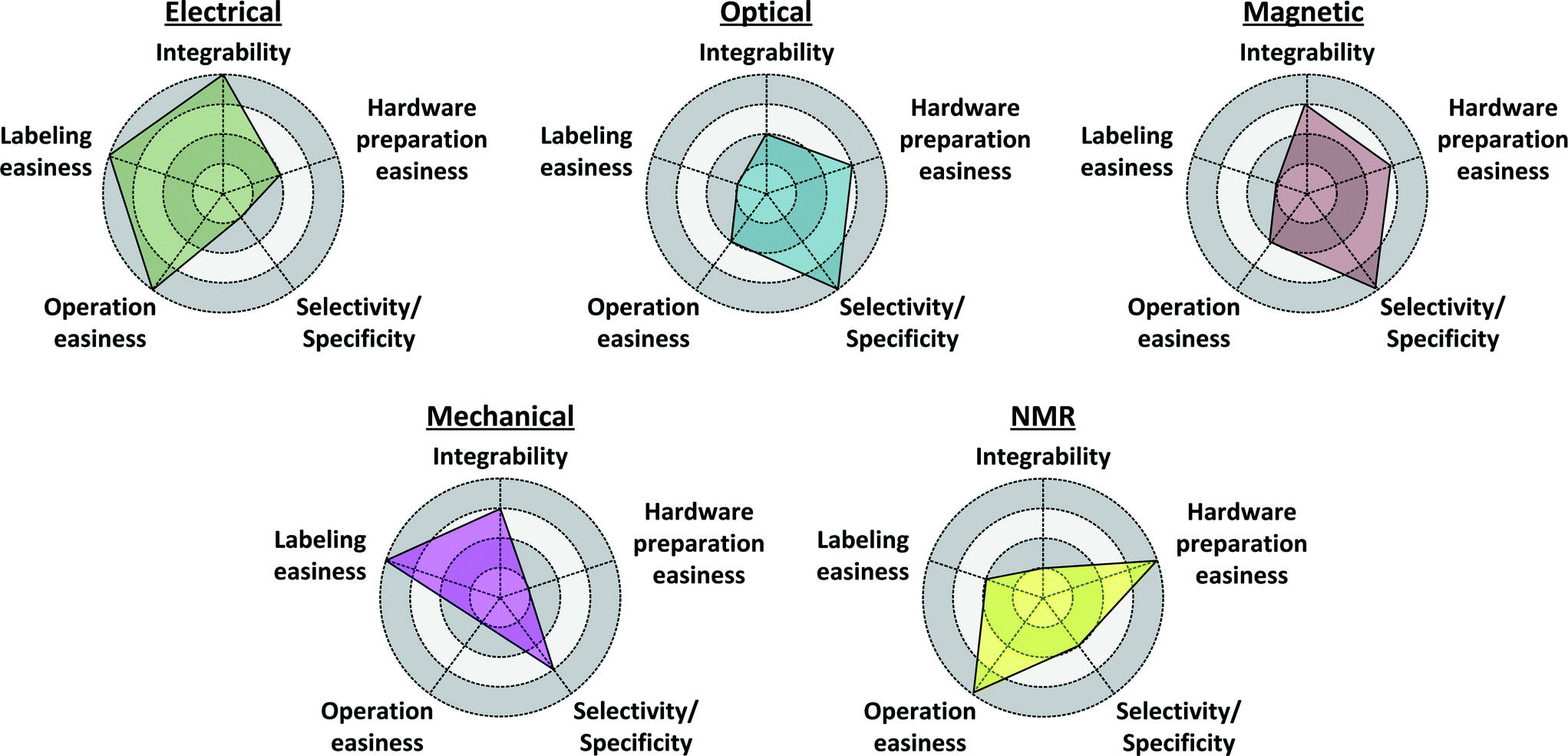 | ||
| Fig. 11 A radar chart showing the conceptual requisites to perform in vitro diagnosis on biomolecule targets with different transducing mechanisms. | ||
V. Conclusions and future prospects
Driven by the world's booming and longevous population in the coming century, there will be a huge market for efficient, low-cost and easy-to-use PoC devices for rapid yet sensitive in vitro diagnosis in both developed and developing countries. CMOS technology offers a platform to implement these IVD tools, which is attributed to its capability for monolithically integrating transducers and signal processing units on the same chip, which can be mass-produced to minimize the cost. Furthermore, benefitting from the continuous improvement of CMOS processes and post-processing techniques, a multifaceted variety of biosensors have been proposed with superior performances. There are different ways to achieve molecular and cellular biosensing on CMOS chips. The necessity and complexity of each transducing mechanism entails a balance of different design goals (e.g., cost) and constraints. Thus, the development of an ideal CMOS biosensor should require profound knowledge, not only in microelectronics, but also in biology and chemistry, to secure successful multi-disciplinary research.The advances in CMOS biosensors will continue with the downscaling of CMOS technology, offering a higher integration level, and better signal processing for a lower detection limit, and supporting more complex operations, such as next-generation sequencing.106 Yet, the post-processing of the CMOS device should be limited and the labelling of the signaling tag should be avoided to suppress the manufacturing cost and the preparation time of the experiments, in order that the overall cost can be competitive with other PoC technologies, such as test-strip devices. Furthermore, it is also of importance to manage the sample matrix effects of biosensors from complex media and include different functions such as multiplexing59 and DNA amplification47,51 in an integrated platform, along with the CMOS biosensors. In addition, as sample management is still a challenge for CMOS chips, extra efforts should be entailed to seamlessly integrate the sample management network and the CMOS biosensor with the aid of channel microfluidic networks107–109 or digital microfluidic arrays,104,110 rendering these CMOS biosensors as truly lab-on-a-chip platforms. In our opinion, these CMOS biosensors will ultimately provide global patients with an efficient and powerful IVD solution to improve their living quality.
Acknowledgements
The authors thank Macao FDCT (SKL fund & 047/2014/A1) and the University of Macau for financial support.References
- D. C. H. Burgess, J. Wasseramn and C. A. Dahl, Nature, 2006, 444(suppl. 1), 1–2 CrossRef PubMed.
- P. Yager, G. J. Domingo and J. Gerdes, Annu. Rev. Biomed. Eng., 2008, 10, 107–144 CrossRef CAS PubMed.
- M. Zuiderwijk, H. J. Tanke, R. Sam Niedbala and P. L. A. M. Corstjens, Clin. Biochem., 2003, 36, 401–403 CrossRef CAS PubMed.
- X. Fu, Z. Cheng, J. Yu, P. Choo, L. Chen and J. Choo, Biosens. Bioelectron., 2016, 78, 530–537 CrossRef CAS PubMed.
- J. Li and J. Macdonald, Lab Chip, 2016, 16, 242–245 RSC.
- J. R. Choi, J. Hu, R. Tang, Y. Gong, S. Feng, H. Ren, T. Wen, X. Li, W. A. B. Wan Abas, B. Pingguan-Murphy and F. Xu, Lab Chip, 2016, 16, 611–621 RSC.
- M. La, S. M. Park and D. S. Kim, Biomicrofluidics, 2015, 9, 014104 Search PubMed.
- B. S. Lee, Y. U. Lee, H.-S. Kim, T.-H. Kim, J. Park, J.-G. Lee, J. Kim, H. Kim, W. G. Lee and Y.-K. Cho, Lab Chip, 2011, 11, 70–78 RSC.
- J. Park, V. Sunkara, T.-H. Kim, H. Hwang and Y.-K. Cho, Anal. Chem., 2012, 84, 2133–2140 CrossRef CAS PubMed.
- W. S. Lee, V. Sunkara, J.-R. Han, Y.-S. Park and Y.-K. Cho, Lab Chip, 2015, 15, 478–485 RSC.
- G. A. Posthuma-Trumpie, J. Korf and A. van Amerongen, Anal. Bioanal. Chem., 2009, 393, 569–582 CrossRef CAS PubMed.
- World development report: making services work for poor people, World Bank, New York, NY, 2004 Search PubMed.
- The top 10 causes of death, http://www.who.int/mediacentre/factsheets/fs310/en/index2.html, (accessed 10th June, 2016) Search PubMed.
- World population prospects: The 2015 revision, United Nations, 2015 Search PubMed.
- A. Palangkaraya and J. Yong, Int. J. Health Care Finance Econ., 2009, 9, 391–402 CrossRef PubMed.
- Z. Miller, Investing in the future of medicine: A investor's guide to the in vitro diagnostics market, http://www.forbes.com/sites/zackmiller/2014/02/12/investing-in-the-future-of-medicine-a-investors-guide-to-the-in-vitro-diagnostics-market/#9d6e5ea5feb4, (accessed 10th June, 2016) Search PubMed.
- S. K. Arya, C. C. Wong, Y. J. Jeon, T. Bansal and M. K. Park, Chem. Rev., 2015, 115, 5116–5158 CrossRef CAS PubMed.
- M. Crescentini, M. Bennati, M. Carminati and M. Tartagni, IEEE Trans. Biomed. Circuits Syst., 2014, 8, 278–292 CrossRef PubMed.
- P. K. Drain, E. P. Hyle, F. Noubary, K. A. Freedberg, D. Wilson, W. R. Bishai, W. Rodriguez and I. V. Bassett, Lancet Infect. Dis., 2014, 14, 239–249 CrossRef PubMed.
- J. P. Lafleur, A. Jönsson, S. Senkbeil and J. P. Kutter, Biosens. Bioelectron., 2016, 76, 213–233 CrossRef CAS PubMed.
- M. Drancourt, A. Michel-Lepage, S. Boyer and D. Raoult, Clin. Microbiol. Rev., 2016, 29, 429–447 CrossRef PubMed.
- N. P. Pai, C. Vadnais, C. Denkinger, N. Engel and M. Pai, PLoS Med., 2012, 9, e1001306 Search PubMed.
- C. P. Y. Chan, W. C. Mak, K. Y. Cheung, K. K. Sin, C. M. Yu, T. H. Rainer and R. Renneberg, Annu. Rev. Anal. Chem., 2013, 6, 191–211 CrossRef CAS PubMed.
- A. Warsinke, Anal. Bioanal. Chem., 2009, 393, 1393–1405 CrossRef CAS PubMed.
- A. Niemz, T. M. Ferguson and D. S. Boyle, Trends Biotechnol., 2011, 29, 240–250 CrossRef CAS PubMed.
- V. Gubala, L. F. Harris, A. J. Ricco, M. X. Tan and D. E. Williams, Anal. Chem., 2012, 84, 487–515 CrossRef CAS PubMed.
- L. Gervais, N. de Rooij and E. Delamarche, Adv. Mater., 2011, 23, H151–H176 CrossRef CAS PubMed.
- J. Schmitz, Nucl. Instrum. Methods Phys. Res., Sect. A, 2007, 576, 142–149 CrossRef CAS.
- C. G. Jakobson, U. Dinnar, M. Feinsod and Y. Nemirovsky, IEEE Sens. J., 2002, 2, 279–287 CrossRef CAS.
- A. H. D. Graham, S. M. Surguy, P. Langlois, C. R. Bowen, J. Taylor and J. Robbins, Biosens. Bioelectron., 2012, 31, 458–462 CrossRef CAS PubMed.
- J. M. Rothberg, W. Hinz, T. M. Rearick, J. Schultz, W. Mileski, M. Davey, J. H. Leamon, K. Johnson, M. J. Milgrew, M. Edwards, J. Hoon, J. F. Simons, D. Marran, J. W. Myers, J. F. Davidson, A. Branting, J. R. Nobile, B. P. Puc, D. Light, T. A. Clark, M. Huber, J. T. Branciforte, I. B. Stoner, S. E. Cawley, M. Lyons, Y. Fu, N. Homer, M. Sedova, X. Miao, B. Reed, J. Sabina, E. Feierstein, M. Schorn, M. Alanjary, E. Dimalanta, D. Dressman, R. Kasinskas, T. Sokolsky, J. A. Fidanza, E. Namsaraev, K. J. McKernan, A. Williams, G. T. Roth and J. Bustillo, Nature, 2011, 475, 348–352 CrossRef CAS PubMed.
- A. Gao, N. Lu, Y. Wang and T. Li, Sci. Rep., 2016, 6, 22554 CrossRef CAS PubMed.
- J. Lee, J. Jang, B. Choi, J. Yoon, J.-Y. Kim, Y.-K. Choi, D. Myong Kim, D. Hwan Kim and S.-J. Choi, Sci. Rep., 2015, 5, 12286 CrossRef PubMed.
- C. Stagni, C. Guiducci, L. Benini, B. Ricco, S. Carrara, B. Samori, C. Paulus, M. Schienle, M. Augustyniak and R. Thewes, IEEE J. Solid-State Circuits, 2006, 41, 2956–2964 CrossRef.
- M. Barbaro, A. Bonfiglio, L. Raffo, A. Alessandrini, P. Facci and I. Barák, Sens. Actuators, B, 2006, 118, 41–46 CrossRef CAS.
- S. J. Han, H. Yu, B. Murmann, N. Pourmand and S. X. Wang, IEEE Int. Solid-State Circuits Conf. (ISSCC) Dig. Tech. Papers, 2007, 168–169 Search PubMed.
- E. Anderson, J. Daniels, H. Yu, T. Lee and N. Pourmand, Proc. Instrum. Meas. Technol. Conf., 2008, 1631–1636 Search PubMed.
- B. Jang, P. Cao, A. Chevalier, A. Ellington and A. Hassibi, IEEE Int. Solid-State Circuits Conf. (ISSCC) Dig. Tech. Papers, 2009, 436–437 Search PubMed.
- T. C. D. Huang, S. Sorgenfrei, P. Gong, R. Levicky and K. L. Shepard, IEEE J. Solid-State Circuits, 2009, 44, 1644–1654 CrossRef PubMed.
- W. Hua, C. Yan, A. Hassibi, A. Scherer and A. Hajimiri, IEEE Int. Solid-State Circuits Conf. (ISSCC) Dig. Tech. Papers, 2009, 438–439 Search PubMed.
- P. M. Levine, P. Gong, R. Levicky and K. L. Shepard, Biosens. Bioelectron., 2009, 24, 1995–2001 CrossRef CAS PubMed.
- A. Manickam, A. Chevalier, M. McDermott, A. D. Ellington and A. Hassibi, IEEE Trans. Biomed. Circuits Syst., 2010, 4, 379–390 CrossRef PubMed.
- H. Jafari, L. Soleymani and R. Genov, IEEE Trans. Biomed. Circuits Syst., 2012, 6, 468–478 CrossRef PubMed.
- K. H. Lee, S. Choi, J. O. Lee, J. B. Yoon and G. H. Cho, IEEE Int. Solid-State Circuits Conf. (ISSCC) Dig. Tech. Papers, 2012, 120–122 Search PubMed.
- M. Barbaro, A. Caboni, D. Loi, S. Lai, A. Homsy, P. D. van der Wal and N. F. de Rooij, Sens. Actuators, B, 2012, 171–172, 148–154 CrossRef CAS.
- Y. J. Huang, C. W. Huang, T. H. Lin, C. T. Lin, L. G. Chen, P. Y. Hsiao, B. R. Wu, H. T. Hsueh, B. J. Kuo, H. H. Tsai, H. H. Liao, Y. Z. Juang, C. K. Wang and S. S. Lu, IEEE Trans. Biomed. Circuits Syst., 2013, 7, 820–831 CrossRef PubMed.
- C. Toumazou, L. M. Shepherd, S. C. Reed, G. I. Chen, A. Patel, D. M. Garner, C.-J. A. Wang, C.-P. Ou, K. Amin-Desai, P. Athanasiou, H. Bai, I. M. Q. Brizido, B. Caldwell, D. Coomber-Alford, P. Georgiou, K. S. Jordan, J. C. Joyce, M. La Mura, D. Morley, S. Sathyavruthan, S. Temelso, R. E. Thomas and L. Zhang, Nat. Methods, 2013, 10, 641–646 CrossRef CAS PubMed.
- C.-W. Huang, Y.-J. Huang, P.-W. Yen, H.-H. Tsai, H.-H. Liao, Y.-Z. Juang, S.-S. Lu and C.-T. Lin, Lab Chip, 2013, 13, 4451–4459 RSC.
- A. Pai, A. Khachaturian, S. Chapman, A. Hu, H. Wang and A. Hajimiri, Analyst, 2014, 139, 1403–1411 RSC.
- H. M. Jafari, K. Abdelhalim, L. Soleymani, E. H. Sargent, S. O. Kelley and R. Genov, IEEE J. Solid-State Circuits, 2014, 49, 1223–1241 CrossRef.
- H. Norian, R. M. Field, I. Kymissis and K. L. Shepard, Lab Chip, 2014, 14, 4076–4084 RSC.
- K. M. Lei, H. Heidari, P. I. Mak, M. K. Law, F. Maloberti and R. P. Martins, IEEE Int. Solid-State Circuits Conf. (ISSCC) Dig. Tech. Papers, 2016, 474–475 Search PubMed.
- C. H. Chen, R. Z. Hwang, L. S. Huang, S. M. Lin, H. C. Chen, Y. C. Yang, Y. T. Lin, S. A. Yu, Y. S. Lin, Y. H. Wang, N. K. Chou and S. S. Lu, IEEE Trans. Biomed. Eng., 2009, 56, 462–470 CrossRef PubMed.
- N. Sun, Y. Liu, H. Lee, R. Weissleder and D. Ham, IEEE J. Solid-State Circuits, 2009, 44, 1629–1643 CrossRef.
- O. Tigli, L. Bivona, P. Berg and M. E. Zaghloul, IEEE Trans. Biomed. Circuits Syst., 2010, 4, 62–73 CrossRef CAS PubMed.
- N. Sun, T. J. Yoon, H. Lee, W. Andress, R. Weissleder and D. Ham, IEEE J. Solid-State Circuits, 2011, 46, 342–352 CrossRef.
- S. Gambini, K. Skucha, P. P. Liu, J. Kim and R. Krigel, IEEE J. Solid-State Circuits, 2013, 48, 302–317 CrossRef.
- D. A. Hall, R. S. Gaster, K. A. A. Makinwa, S. X. Wang and B. Murmann, IEEE J. Solid-State Circuits, 2013, 48, 1290–1301 CrossRef PubMed.
- L. Sandeau, C. Vuillaume, S. Contie, E. Grinenval, F. Belloni, H. Rigneault, R. M. Owens and M. B. Fournet, Lab Chip, 2015, 15, 877–881 RSC.
- C. Sapsanis, S. Sivashankar, H. Omran, U. Buttner and K. N. Salama, Proc IEEE Int. Midwest Symp. Circuits Syst., 2015, 1–4 Search PubMed.
- L. Y. Hong, S. McManus, H. Yang and K. Sengupta, Proc. Symp. VLSI circuits, 2015, C206–C207 Search PubMed.
- P. H. Kuo, J. C. Kuo, H. T. Hsueh, J. Y. Hsieh, Y. C. Huang, T. Wang, Y. H. Lin, C. T. Lin, Y. J. Yang and S. S. Lu, IEEE Trans. Biomed. Circuits Syst., 2015, 9, 790–800 Search PubMed.
- H. Klapproth, S. Bednar, J. Baader, M. Lehmann, I. Freund, T. Brandstetter and J. Rühe, Sens. Biosensing Res., 2015, 5, 117–122 CrossRef.
- Y. Zheng, N. Shang, P. S. Haddad and M. Sawan, IEEE Trans. Biomed. Circuits Syst., 2016, 10, 477–486 CrossRef PubMed.
- S. B. Prakash and P. Abshire, IEEE Sens. J., 2007, 7, 440–447 CrossRef.
- S. B. Prakash and P. Abshire, Biosens. Bioelectron., 2008, 23, 1449–1457 CrossRef CAS PubMed.
- E. P. Dupont, E. Labonne, Y. Maruyama, C. Vandevyver, U. Lehmann, M. A. M. Gijs and E. Charbon, Sens. Actuators, B, 2012, 174, 609–615 CrossRef CAS.
- Y. Chen, C. C. Wong, T. S. Pui, R. Nadipalli, R. Weerasekera, J. Chandran, H. Yu and A. R. A. Rahman, Sens. Actuators, B, 2012, 173, 903–907 CrossRef CAS.
- K. H. Lee, J. Nam, S. Choi, H. Lim, S. Shin and G. H. Cho, IEEE Int. Solid-State Circuits Conf. (ISSCC) Dig. Tech. Papers, 2012, 304–306 Search PubMed.
- H. Wang, A. Mahdavi, D. A. Tirrell and A. Hajimiri, Lab Chip, 2012, 12, 4465–4471 RSC.
- T. Saeki, M. Hosokawa, T. Lim, M. Harada, T. Matsunaga and T. Tanaka, PLoS One, 2014, 9, e89011 Search PubMed.
- P. Murali, I. Izyumin, D. Cohen, J. C. Chien, A. M. Niknejad and B. Boser, IEEE Int. Solid-State Circuits Conf. (ISSCC) Dig. Tech. Papers, 2014, 422–423 Search PubMed.
- M. Roy, G. Jin, D. Seo, M.-H. Nam and S. Seo, Sens. Actuators, B, 2014, 201, 321–328 CrossRef CAS.
- K. Niitsu, S. Ota, K. Gamo, H. Kondo, M. Hori and K. Nakazato, IEEE Trans. Biomed. Circuits Syst., 2015, 9, 607–619 CrossRef PubMed.
- C. Laborde, C. Pittino, H. A. Verhoeven, S. G. Lemay, L. Selmi, M. A. Jongsma and F. P. Widdershoven, Nat. Nanotechnol., 2015, 10, 791–795 CrossRef CAS PubMed.
- T. Chi, J. S. Park, J. C. Butts, T. A. Hookway, A. Su, C. Zhu, M. P. Styczynski, T. C. McDevitt and H. Wang, IEEE Trans. Biomed. Circuits Syst., 2015, 9, 801–814 CrossRef PubMed.
- K. T. Chang, Y. J. Chang, C. L. Chen and Y. N. Wang, Electrophoresis, 2015, 36, 413–419 CrossRef CAS PubMed.
- J. C. Love, L. A. Estroff, J. K. Kriebel, R. G. Nuzzo and G. M. Whitesides, Chem. Rev., 2005, 105, 1103–1169 CrossRef CAS PubMed.
- A. Manickam, C. A. Johnson, S. Kavusi and A. Hassibi, Sensors, 2012, 12, 14467 CrossRef CAS PubMed.
- C. Berggren, P. Stalhandske, J. Brundell and G. Johansson, Electroanalysis, 1999, 11, 156–160 CrossRef CAS.
- J. Enderlein, T. Ruckstuhl and S. Seeger, Appl. Opt., 1999, 38, 724–732 CrossRef CAS PubMed.
- M. Alvarez and L. M. Lechuga, Analyst, 2010, 135, 827–836 RSC.
- H. Wohltjen and R. Dessy, Anal. Chem., 1979, 51, 1458–1464 CrossRef CAS.
- C. Min, H. L. Shao, M. Liong, T. J. Yoon, R. Weissleder and H. Lee, ACS Nano, 2012, 6, 6821–6828 CrossRef CAS PubMed.
- L. Josephson, J. M. Perez and R. Weissleder, Angew. Chem., 2001, 113, 3304–3306 CrossRef.
- J. M. Perez, L. Josephson, T. O'Loughlin, D. Hogemann and R. Weissleder, Nat. Biotechnol., 2002, 20, 816–820 CrossRef CAS PubMed.
- H. Lee, E. Sun, D. Ham and R. Weissleder, Nat. Med., 2008, 14, 869–874 CrossRef CAS PubMed.
- I. Koh, R. Hong, R. Weissleder and L. Josephson, Angew. Chem., Int. Ed., 2008, 47, 4119–4121 CrossRef CAS PubMed.
- D. Issadore, C. Min, M. Liong, J. Chung, R. Weissleder and H. Lee, Lab Chip, 2011, 11, 2282–2287 RSC.
- M. Liong, A. N. Hoang, J. Chung, N. Gural, C. B. Ford, C. Min, R. R. Shah, R. Ahmad, M. Fernandez-Suarez, S. M. Fortune, M. Toner, H. Lee and R. Weissleder, Nat. Commun., 2013, 4, 1–9 Search PubMed.
- C. M. Castro, A. A. Ghazani, J. Chung, H. L. Shao, D. Issadore, T. J. Yoon, R. Weissleder and H. Lee, Lab Chip, 2014, 14, 14–23 RSC.
- E. Engvall and P. Perlmann, Immunochemistry, 1971, 8, 871–874 CrossRef CAS PubMed.
- R. W. Peeling, H. Artsob, J. L. Pelegrino, P. Buchy, M. J. Cardosa, S. Devi, D. A. Enria, J. Farrar, D. J. Gubler, M. G. Guzman, S. B. Halstead, E. Hunsperger, S. Kliks, H. S. Margolis, C. M. Nathanson, V. C. Nguyen, N. Rizzo, S. Vazquez and S. Yoksan, Nat. Rev. Microbiol., 2010, S30–S37 CrossRef CAS.
- N. Scholler, M. Crawford, A. Sato, C. W. Drescher, K. C. O'Briant, N. Kiviat, G. L. Anderson and N. Urban, Clin. Cancer. Res., 2006, 12, 2117–2124 CrossRef CAS PubMed.
- S. Velumani, H.-T. Ho, F. He, S. Musthaq, M. Prabakaran and J. Kwang, PLoS One, 2011, 6, e20737 CAS.
- C. Kandoth, M. D. McLellan, F. Vandin, K. Ye, B. Niu, C. Lu, M. Xie, Q. Zhang, J. F. McMichael, M. A. Wyczalkowski, M. D. M. Leiserson, C. A. Miller, J. S. Welch, M. J. Walter, M. C. Wendl, T. J. Ley, R. K. Wilson, B. J. Raphael and L. Ding, Nature, 2013, 502, 333–339 CrossRef CAS PubMed.
- M. Schena, D. Shalon, R. W. Davis and P. O. Brown, Science, 1995, 270, 467–470 CAS.
- H. Shafiee, S. Wang, F. Inci, M. Toy, T. J. Henrich, D. R. Kuritzkes and U. Demirci, Annu. Rev. Med., 2015, 66, 387–405 CrossRef CAS PubMed.
- J. L. Arlett, E. B. Myers and M. L. Roukes, Nat. Nanotechnol., 2011, 6, 203–215 CrossRef CAS PubMed.
- T. Bryan, X. Luo, P. R. Bueno and J. J. Davis, Biosens. Bioelectron., 2013, 39, 94–98 CrossRef CAS PubMed.
- J. T. Kirk, N. D. Brault, T. Baehr-Jones, M. Hochberg, S. Jiang and D. M. Ratner, Biosens. Bioelectron., 2013, 42, 100–105 CrossRef CAS PubMed.
- K. R. Thulborn, J. C. Waterton, P. M. Matthews and G. K. Radda, Biochim. Biophys. Acta, 1982, 714, 265–270 CrossRef CAS.
- E. Ghafar-Zadeh and M. Sawan, IEEE Trans. Biomed. Circuits Syst., 2007, 1, 270–277 CrossRef CAS PubMed.
- K.-M. Lei, P.-I. Mak, M.-K. Law and R. P. Martins, Analyst, 2015, 140, 5129–5137 RSC.
- W. K. Peng, T. F. Kong, C. S. Ng, L. Chen, Y. Huang, A. A. S. Bhagat, N.-T. Nguyen, P. R. Preiser and J. Han, Nat. Med., 2014, 20, 1069–1073 CrossRef CAS PubMed.
- D. A. Hall, J. S. Daniels, B. Geuskens, N. Tayebi, G. M. Credo, D. J. Liu, H. Li, K. Wu, X. Su, M. Varma and O. H. Elibol, IEEE Int. Solid-State Circuits Conf. (ISSCC) Dig. Tech. Papers, 2016, 288–289 Search PubMed.
- Y. Huang and A. J. Mason, Lab Chip, 2013, 13, 3929–3934 RSC.
- R. R. Singh, L. Leng, A. Guenther and R. Genov, IEEE J. Solid-State Circuits, 2012, 47, 2822–2833 CrossRef.
- X. Liu, L. Li and A. J. Mason, Philos. Trans. R. Soc., A, 2014, 372 CAS.
- G. Wang, D. Teng, Y. T. Lai, Y. W. Lu, Y. Ho and C. Y. Lee, IET Nanobiotechnol., 2014, 8, 163–171 CrossRef CAS PubMed.
| This journal is © The Royal Society of Chemistry 2016 |