
 Open Access Article
 This Open Access Article is licensed under a Creative Commons Attribution-Non Commercial 3.0 Unported Licence
In-mold patterning and actionable axo-somatic compartmentalization for on-chip neuron culture†
Ayako
Yamada‡
ab,
Maéva
Vignes‡
abc,
Cécile
Bureau
ab,
Alexandre
Mamane
ab,
Bastien
Venzac
ab,
Stéphanie
Descroix
ab,
Jean-Louis
Viovy
ab,
Catherine
Villard
*abd,
Jean-Michel
Peyrin
*c and
Laurent
Malaquin
*abe
aInstitut Curie, PSL Research University, CNRS, UMR 168, F-75005, Paris, France. E-mail: catherine.villard@curie.fr (CV); laurent.malaquin@laas.fr (LM)
bSorbonne Universités, UPMC Univ Paris 06, CNRS, UMR 168, F-75005, Paris, France
cUPMC Univ Paris 06, CNRS, UMR 8256, B2A, Sorbonne Universités, Biological Adaptation and Ageing, Institut de Biologie Paris Seine, Paris, F-75005, France. E-mail: jean-michel.peyrin@upmc.fr (JMP)
dCNRS, Inst NEEL and CRETA, Univ. Grenoble Alpes, F-38042 Grenoble, France
eLAAS-CNRS, Université de Toulouse, CNRS, Toulouse, France. E-mail: jean-michel.peyrin@upmc.fr
First published on 26th April 2016
Abstract
Oriented neuronal networks with controlled connectivity are required for many applications ranging from studies of neurodegeneration to neuronal computation. To build such networks in vitro, an efficient, directed and long lasting guidance of axons toward their target is a pre-requisite. The best guidance achieved so far, however, relies on confining axons in enclosed microchannels, making them poorly accessible for further investigation. Here we describe a method providing accessible and highly regular arrays of axons, emanating from somas positioned in distinct compartments. This method combines the use of a novel removable partition, allowing soma positioning outside of the axon guidance patterns, and in-mold patterning (iMP), a hybrid method combining chemical and mechanical cell positioning clues applied here for the first time to neurons. The axon guidance efficiency of iMP is compared to that of conventional patterning methods, e.g. micro-contact printing (chemical constraints by a poly-L-lysine motif) and micro-grooves (physical constraints by homogeneously coated microstructures), using guiding tracks of different widths and spacing. We show that iMP provides a gain of 10 to 100 in axon confinement efficiency on the tracks, yielding mm-long, highly regular, and fully accessible on-chip axon arrays. iMP also allows well-defined axon guidance from small populations of several neurons confined at predefined positions in μm-sized wells. iMP will thus open new routes for the construction of complex and accurately controlled neuronal networks.
Introduction
The complex ramified morphology of cultured neurons raises difficulties in analyzing their behaviors or in constructing artificial neuronal networks of controlled axo-dendritic polarity. In the past decades, strong efforts have thus been made to control neuronal morphologies.1 Methods derived from soft lithography2 are particularly suited to build substrates with micro-scale features specifically designed to direct the shape of neurons. Micro-contact printing (μCP) techniques, in which micro-patterns of biomolecules are printed on flat substrates, have been applied for controlling the morphology of neurons.3,4 They provide chemical constraints on neuronal morphologies, by making a contrast of cell adhesion properties inside and outside the micro-patterns. Other groups used physical constraints on neurons, such as topographical barriers in the form of micro-grooves5–7 or micro-pillars.8,9 However, by applying a sole chemical or physical constraint, achieving a long-term and efficient confinement of neurons on μm-sized motifs remains challenging.6,7,10,11 To further improve neuron confinement, the combination of chemical and physical constraints, referred to as hybrid constraint, has also been explored. For instance, Zhang et al. used topographical barriers with a partial chemical treatment only at the bottom of the structures.12 However, the authors observed that axons climbed over the barriers made of a photoresist, to which axons could adhere even without surface treatment. In a different context, Biancardo et al. had proposed another method to prepare substrates with hybrid constraints, referred to as in-mold patterning (iMP).13,14 It constitutes transferring both protein micro-patterns and microstructures simultaneously from a mold to the final substrate, thanks to a step in which the protein is deposited on the protruding part of the microstructures of the mold. Here we propose to adapt this method by replacing polymer melts with polydimethylsiloxane (PDMS) for easy handling and versatility, and apply it to neurons for improved control over their morphology.Besides the difficulties discussed above, regarding the quality of axon guidance, the preparation of well-controlled neuron arrays faces another challenge, associated with the relative positioning of somas with regard to the axon guidance tracks. Axon guidance in combination with soma positioning has been achieved by several strategies. For instance, micro-patterns of cell adhesive molecules,10,15–18 cell repellent layers,19 or a modifiable microstructure in agarose gel20 have been proposed, but they are limited to single or a few neurons. For larger neuron populations, Park et al. combined PDMS compartments with a micro-grooved substrate to obtain an open array of axons with soma positioning, but long-term axon confinement was not demonstrated.7 In addition to these strategies, stencil seeding techniques,21 or laminar structures of hydrogel in a microfluidic channel22 provide soma positioning but not axon guidance.
A more satisfactory solution to the problem of somato-axonal segregation was provided by microfluidics.23 In the last few years, the development of various microfluidic platforms has considerably increased the ability of creating deterministic neuron arrays.24–27 In such platforms, axons were separated from somas and guided by narrow and closed microchannels with their height smaller than that of somas, thus allowing a full exclusion of somas from the guiding tracks. By using funnel-shaped microchannels, this technique also permitted the mastering of a directional connectivity between two populations.26 However, all these approaches share the limitations of strongly confining axons in narrow microchannels, resulting in poor accessibility of the guided axons, and nutrition problems for long-term viability of the axons.
Combining a full spatial separation between somato-dendritic and axonal compartments with a long-term confinement of axons in high-density neuron cultures, while keeping all cellular compartments in an open microenvironment to allow physical, biochemical, and cellular addressing, thus remains an unmet challenge. Here, we address this challenge using a novel microfilament-integrated microfluidic chip. The microfilament serves as a removable wall, thus allowing post-seeding reconfiguration of the partition of the microfluidic platform.28 The partition separates the seeding chamber from axon guiding tracks during soma positioning, enabling a well-defined control of soma positioning without the high confinement limit imposed by microchannels in earlier methods.24–27 We combine this approach with a modified and optimized iMP, and compare it regarding axon guidance efficiency with two more conventional techniques: μCP and topographical constraint in the form of micro-grooves (μGro). All the substrates are made of a thin layer of PDMS with (μGro, iMP) or without (μCP) 5 μm-high microstructures. Substrates are coated with fluorescein isothiocyanate-labeled poly-L-lysine (PLL-FITC) partially (μCP, iMP) or homogeneously (μGro) for cell adhesion, as depicted in Fig. 1 (green color). Overall, we show that the iMP technique achieves a much better long-term confinement of axons originating from a large or small neuronal population, thus paving the way for reconstituting highly deterministic neuronal networks. Systematic studies, varying geometrical parameters, allow us to explore and discuss the mechanisms of confinement and provide guidelines for optimizing micro-pattern geometries.
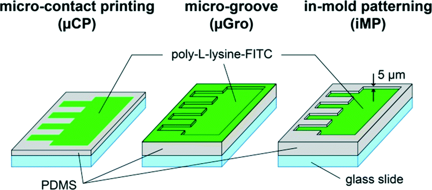 | ||
| Fig. 1 Scheme of the three different substrates for axon guidance. The micro-contact printing (μCP) substrate consists of a micro-pattern of poly-L-lysine-FITC (PLL-FITC) on a flat surface, which works as a chemical constraint for axons (left). The micro-groove (μGro) substrate consists of 5 μm-high micro-structures with homogeneous PLL-FITC coating, providing a topographical constraint for axons (middle). The in-mold patterning (iMP) substrate is a hybrid substrate with 5 μm-high micro-structures with PLL-FITC coating at the bottom of the structure only (right).The surface areas coated with PLL-FITC are indicated with green color. | ||
Materials and methods
All reagents were purchased from Sigma-Aldrich unless otherwise specified.Preparation of axon guiding substrates
![[thin space (1/6-em)]](https://www.rsc.org/images/entities/char_2009.gif) :1 (w/w) and degassed prior to use, on a glass cover slip (0.13–0.16 mm thick) by a spin-coater (SPIN150, SPS-Europe) at 3000 rpm for 60 s and incubating at 66 °C overnight. The thickness of the PDMS layer was measured to be 28 ± 1 μm by a profilometer (Wyko NT1100, Veeco). To better transfer PLL-FITC from the PDMS stamp to the substrate, which is hydrophobic by nature, the substrate surface was turned to a high energy surface by plasma treatment using an air plasma cleaner (Harrick) immediately before printing.
:1 (w/w) and degassed prior to use, on a glass cover slip (0.13–0.16 mm thick) by a spin-coater (SPIN150, SPS-Europe) at 3000 rpm for 60 s and incubating at 66 °C overnight. The thickness of the PDMS layer was measured to be 28 ± 1 μm by a profilometer (Wyko NT1100, Veeco). To better transfer PLL-FITC from the PDMS stamp to the substrate, which is hydrophobic by nature, the substrate surface was turned to a high energy surface by plasma treatment using an air plasma cleaner (Harrick) immediately before printing.
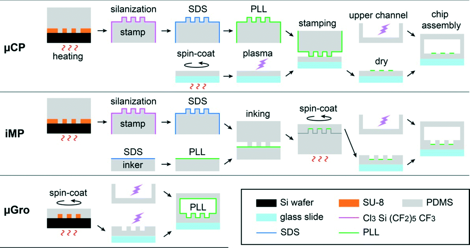 | ||
| Fig. 2 Scheme for the preparation of the three different substrates and microfluidic chip assembly. The thickness of all the SU-8 layers is 5 μm. | ||
The mold for the PDMS stamp was fabricated by photolithography as follows. A 5 μm-thick layer of SU-8 2005 (MicroChem) was formed on a 2 inch silicon wafer (Neyco) by spin-coating at 3000 rpm for 30 s. After a soft bake, the wafer was exposed to UV light (MJB4 Mask Aligner, SUSS MicroTec) through a hard chromium mask or a flexible transparency mask (Selba S. A.) depending on the required resolutions prior to a post exposure bake, and developed using SU-8 developer (MicroChem). The obtained mold was exposed to a vapor of trimethylchlorosilane (TMCS, ABCR GmbH & Co. KG) for 5 min once, and used repeatedly without further treatment. PDMS was mixed with its linker, poured onto the mold, degassed under vacuum, and reticulated at 66 °C for at least 4 h. A PDMS block, about 3 mm thick, was cut off from the mold and used as a stamp. The stamp was soaked in 96% ethanol for 24 h, dried at 66 °C overnight, and plasma treated prior to the exposure to a vapor of (tridecafluoro-1,1,2,2-tetrahydrooctyl)trichlorosilane (ABCR GmbH & Co. KG) in a depressurized desiccator for 20 min. This silanization step prevented the stamp surface from binding to the plasma treated substrate during the following stamping process. The stamp was incubated in 10% (w/v) sodium dodecyl sulfate (SDS, Euromedex) in MilliQ water for 20 min to decorate the hydrophobic stamp surface with negative charges and to enhance PLL-FITC transfer from the stamp to the substrate,31 rinsed 3 times with MilliQ water, and incubated with 0.01 mg mL−1 PLL-FITC in Dulbecco's phosphate buffered saline (DPBS) without CaCl2 and MgCl2 for 1 h at room temperature. After being rinsed with water and dried by pressurized air flow, the stamp was carefully laid down on the plasma treated substrate with its microstructured side down. A 30 g flat weight was put on the stamp for 3 min and removed. The substrate, together with the stamp on it, was aligned under the microscope on a printed paper reproducing the exact shape of a microfluidic channel (see below). The substrate was maintained with Scotch removable tapes (3M) on this paper template. This step was essential in order to have a reference in terms of positioning for the final mounting of the channel on the micro-printed substrate. The stamp was then removed from the substrate and discarded. The substrate was dried at room temperature overnight. The retention of the PLL-FITC micro-pattern was strongly improved by the drying process, while the non-covered substrate surface returned back to the hydrophobic state during drying. Indeed, we could not obtain a clear PLL-FITC micro-pattern when the substrate was immersed in a buffer immediately after printing. This implies that the drying process promotes the physisorption of PLL-FITC on the substrate.
Geometry of micro-patterns on the photomask
All the micro-patterns on the photomasks used for the mold preparation of μCP, iMP and μGro substrates contained a 900 μm × 8 mm rectangle, which resulted in a cell seeding area homogeneously coated with PLL-FITC on the final substrates. From one of the long sides of the rectangle, 1 mm-long, straight, and parallel lines with different widths (w = 5, 10, 20, 40, and 80 μm) and intervals (d = 5, 10, 20, 40, and 80 μm), which served as axon guiding tracks, projected out perpendicularly to the rectangle. The length of the rectangle was divided into several 700 μm-long blocks corresponding to a given pair of (w, d) values (see Fig. 3, bottom right). We used a chromium mask for the micro-patterns containing structures characterized by d or w equal to 5 μm, and a transparency mask with a resolution of 50800 dpi for the others. Importantly, for μCP and iMP, the background outside the micro-patterns was filled with 50 μm-diameter disks arranged at 100 μm pitch. These disks resulted in pillars on the PDMS stamps, which prevented the stamps from collapsing on the substrate.
 | ||
| Fig. 3 Scheme of the microfluidic chip for cell culture and axon guidance. An 80 μm-high microfluidic channel with 4 reservoirs, equipped with a removable partition made of a fishing line, was aligned and bound on an axon guiding substrate (left). Cells were settled on a cell seeding area next to axon guiding tracks, separated by the partition. The latter was removed 1 hour after cell seeding (right). | ||
Microfluidic chip preparation
Density of PLL coating according to the different types of substrates
As described above, PLL-FITC was directly incubated on μGro samples, while it was transferred between PDMS surfaces once and twice for μCP and iMP, respectively, during substrate preparation. These different protocols yielded different coating densities on the final chip, as displayed in ESI† Fig. S1a. The PLL-FITC density was the highest on μCP samples, and the lowest for the iMP technique with a reduction of a factor of 5 compared to μCP. The spatial distribution of PLL-FITC was also assessed for the three different techniques, showing that the finer, i.e. 5 μm wide micro-pattern separated by 5 μm interval was successfully obtained (ESI† Fig. S1b) and that the PLL-FITC layer was uniform in all techniques (ESI† Fig. S1c–e).Cell culture
The study was carried out in accordance with European Community guidelines on the care and use of laboratory animals: 86/609/EEC. Cortices were dissected under a microscope from E17 embryos of Oncins France 1 mouse (Charles River) in Gey's balanced salt solution supplemented with 0.1% glucose (w/v). After rinsing, the cortices were incubated for 15 min at 37 °C with 20 U mL−1 papain and 0.6 mg mL−1 cysteine in DMEM supplemented with 100 U mL−1 penicillin–streptomycin. After deactivating papain by adding one-tenth volume of FBS, followed by 5 min incubation at room temperature and rinsing with DMEM, cortical cells were mechanically dissociated by pipetting in DMEM containing 40 U mL−1 deoxyribonuclease I. The cells were rinsed twice with DMEM and suspended in complete culture medium (see above) at 3 × 10⁷ cells mL−1. After removal of the medium from the reservoirs of the microfluidic chip, 2 μL each of the cell suspension and complete medium were introduced simultaneously into the chip from one reservoir on the cell-seeding-area side and from the next one on the micro-patterned side, respectively. The chip was incubated in the CO2 incubator at 37 °C with 5% CO2 for 10 min to make the cells sediment and attach onto the substrate, and then each reservoir of the chip was filled with 40 μL of complete culture medium. The chip was enclosed in the plastic box described above to avoid evaporation, and placed in the CO2 incubator. One hour after cell seeding, one extremity of the fishing line was cut off at the exit from the PDMS block, and the line was removed from the chip by pulling the other extremity with tweezers. Cells were cultured for 6 or 11 days in the incubator, as previously described.26 For 11 days culture, complete medium was renewed on the 6th day.Immunofluorescence staining and imaging
After removal of the culture medium from the reservoirs of the chip, 4% paraformaldehyde (Electron Microscopy Sciences, v/v) in DPBS supplemented with 4% sucrose (w/v) was introduced into the channel for cell fixation, using a slight gradient of hydrostatic pressure in the longitudinal direction. For that purpose, 30 μL of solution was added to each upstream reservoir, and 20 μL to the downstream ones, using an automatic pipette (Finnpipette, Thermo Scientific). The chip was incubated for 10 min at room temperature and rinsed with DPBS. DPBS containing 1% bovine serum albumin (w/v) and 0.1% Triton-X (Life Technologies, v/v) was introduced into the chip with a hydrostatic pressure gradient as described above, and incubated for 45 min at room temperature. After rinsing with DPBS, a primary antibody solution containing anti-microtubule-associated protein 2 (MAP2) antibody (EMD Millipore, rabbit polyclonal, 1/300 volume fraction) and anti-Tau antibody (EMD Millipore, mouse monoclonal, 1/300) in DPBS was introduced into the channel with a gradient (20 μL each to the upstream reservoirs and 15 μL each to the downstream ones) and incubated overnight at 4 °C. After rinsing with DPBS, a secondary antibody solution containing Alexa Fluor 546-conjugated anti-rabbit IgG antibody (Life Technologies, goat polyclonal, 1/200), Alexa Fluor 647-conjugated anti-mouse IgG antibody (Life Technologies, goat polyclonal, 1/200), and 1 μg mL−1 Hoechst (Life Technologies) in DPBS was introduced in the same manner as the primary antibody solution, and incubated for 2 h at room temperature. After rinsing twice with DPBS, the sample was observed by a fluorescence microscope (Eclipse Ti, Nikon) equipped with a CCD camera (CoolSNAP HQ2, Photometrics) through a 4× objective or by a confocal microscope (LSM 510 Meta, Zeiss) through 40× and 63× objectives, with sealing the reservoirs with 10 μL each of mineral oil. Images were analyzed with ImageJ software.Results
All types of substrates yielded similar maximal axonal lengths integrated over 6 DIV (ESI† Fig. S2a, b), indicating that the growth rate is not compromised by the significant reduction in the density of PLL coating associated with iMP (ESI† Fig. S1a). Similarly, we did not observe any difference in the density of somas attached in the seeding areas of the different types of substrates (ESI† Fig. S2c). This suggests that even in iMP, the lower density of PLL is not detrimental to cell soma adhesion. However, the extent and the characteristics of the confinement differ from one constraint to the other, as revealed by different behaviors occurring (i) between the tracks, (ii) at the track ends and (iii) along the tracks. Qualitative and quantitative analyses of these differences in axonal confinement are provided below.Frequency of barrier crossing
The most dramatic difference between techniques is revealed quantitatively at 11 DIV (see Fig. 4a for immunofluorescence images of neurons at 11 DIV in the case of 5 μm-wide tracks with 5 μm intervals) by the variation in the number of barrier crossing events per unit length, nc, depending on the interval of stripes, d. To evaluate nc, the length of the part of a track filled with axons, i.e. L, was first measured. Then, for the simplicity of the measurement, the number of axons escaping from the track on both sides as ‘branches’, nb, was counted regardless of whether or not the axons were reaching the next track (see the scheme of this measurement in Fig. 4b). The parts of a track where crossing events were affected by extrinsic factors or finite-size effects were excluded from the measurement. This corresponds for instance to axons reflected at the end of a track (seen in μCP and μGro), or rare cases in which axons grew on a barrier directly from a soma positioned on the barrier (seen in μCP and μGro), or perturbation of axon growth by glial cells on the barrier (seen in μGro). The average number of crossings per length was finally defined as nc = ∑nb/(2∑L), since the number of crossings could be roughly estimated as nb/2 (e.g. an axon totally crossing the barrier, corresponding to nc = 1, has nb = 1 on one track and nb = 1 on the next track). The summation was taken over a large number of samples from the same dissection so that ∑nb became non-zero.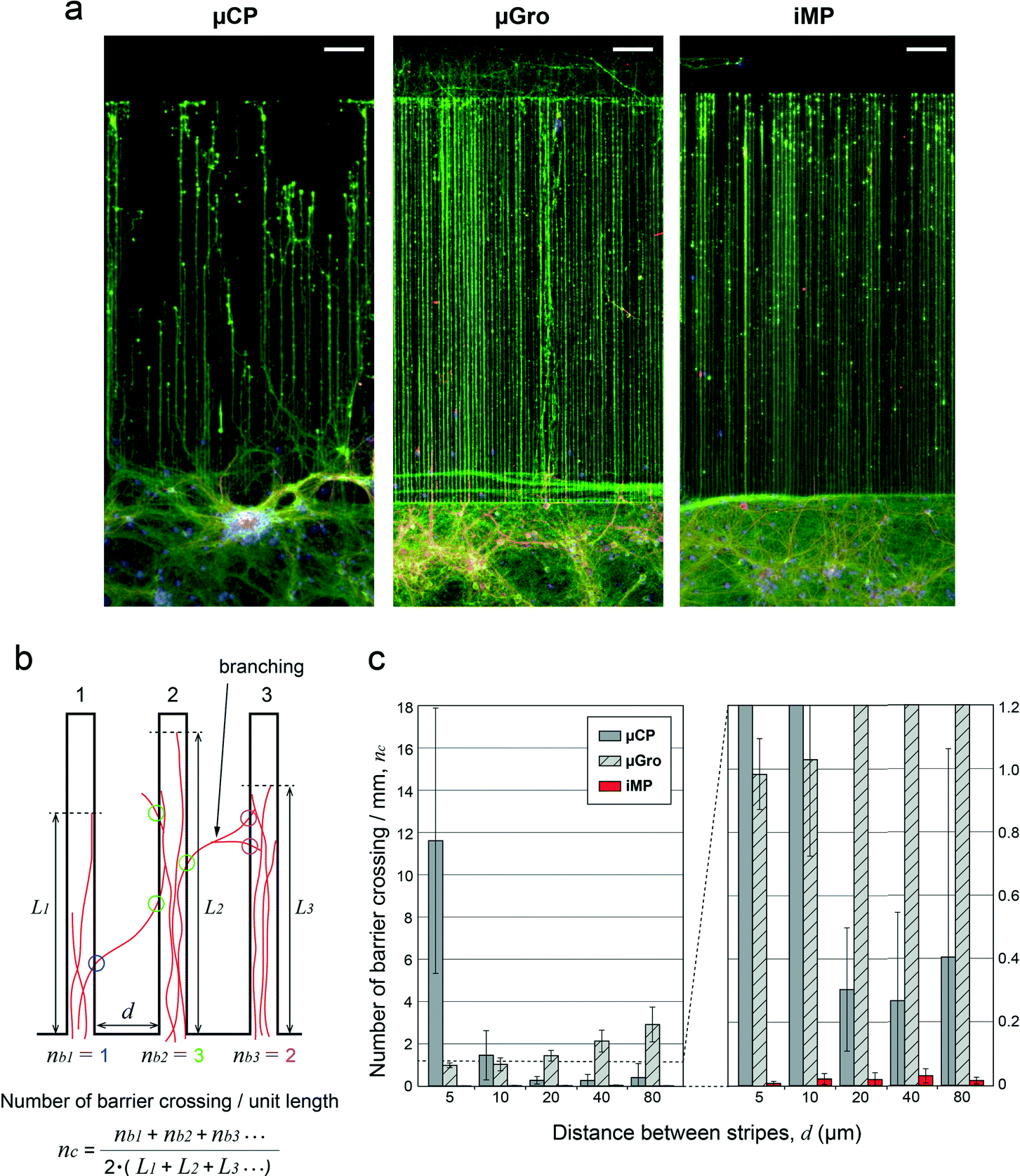 | ||
| Fig. 4 Efficiency of axon confinement in the tracks. (a) Immunofluorescence images of neurons at 11 DIV on different substrates with 5 μm-wide guiding tracks with 5 μm intervals. Axons (green), dendrites (red), and nuclei (blue) are stained by using anti-Tau, anti-MAP2 antibodies, and Hoechst, respectively. Scale bars, 100 μm. (b) Scheme of the counting of the number of barrier crossing events per unit length, nc (left). (c) nc is displayed against the track interval, d, for the different techniques. iMP shows a remarkably high efficiency of axon confinement. For d = 5, 10, 20, 40, and 80 μm, the number of samples are: n = 104, 319, 268, 153, and 92 (μCP); n = 463, 337, 259, 153, and 119 (μGro); n = 533, 476, 266, 167, and 120 (iMP), respectively. Error bars represent standard deviations. | ||
Fig. 4c shows the values of nc, averaged among 2 to 5 sample groups from independent dissections, depending on d for different substrates. The values of nc for iMP are 1 to 2 orders of magnitude smaller than those for the other techniques, proving that iMP has by far the highest efficiency of axon confinement among these substrates. In the case of μCP, nc is high relative to any other situations when the track interval, i.e. barrier length, d is 5 μm. It is still significant for d = 10 μm, and then drops for higher d values. We associate this poor efficiency at low spacing with the capability of filipodia to explore 2D areas even in the absence of PLL coating. This assumption is consistent with an earlier work that estimated a filipodia length around 5 μm.33 For μGro, nc is higher than that for iMP for all values of d, and becomes larger than that for μCP for d ≥ 10 μm. This limited confinement effect indicates that the 5 μm-high obstacle provided by the border is easily crossed by axons when the whole chip surface is adhesive, in agreement with previous results.34 The increase of nc with the increase of d in μGro can be simply explained by the fact that the larger is d, the higher is the probability that an axon branches before reaching the next track (as shown in the scheme of Fig. 4b). This last analysis also provides a measure of the characteristic length between axonal branching points, about 40 μm, also in agreement with previous observations.35
In the case of iMP, nc is remarkably small (nc = 0.009, 0.018, 0.022, 0.033, and 0.015 per mm for d = 5, 10, 20, 40, and 80 μm, respectively) and axons very rarely escape from tracks. Note that iMP at d = 5 μm gives nc values one order of magnitude smaller than those of μCP at d = 20 μm, whereas the cross-sectional contour length of the 5 μm-high barrier at d = 5 μm, i.e. 15 μm (representing the transverse length axons must cross in order to jump from one groove to the other), is smaller than 20 μm. This provides direct evidence that a non-coated topographical barrier strongly improves the confinement efficiency, and is more efficient in that respect than increasing the length of a flat, non-coated interval between tracks. Conversely, it has been shown that when only topographical barriers with cell adhesive surfaces, as in the μGro condition, are applied, 25 μm-high walls are necessary to achieve a high efficiency confinement in tracks.6,34 By combining both chemical and topographical constraints, we succeeded in drastically improving the guidance and confinement efficiency.
Fate of axons at the track ends
Typical behaviors associated with each type of constraints are observed when axons reach the track ends, as shown in Fig. 5a. In the case of μCP, axons tend to keep on growing by turning at a right angle and jumping from one neighboring track to the other. This phenomenon is associated with a relatively higher probability of crossing of the non-adhesive areas between PLL-coated stripes for μCP, as described in the previous section. In the case of μGro, axons are allowed to continue their growth out from the tracks due to the homogenous PLL-FITC coating. Interestingly, axons show a directional persistency outside the grooves. In contrast, in the condition of iMP, axons stop at the walls located at the end of the tracks. This is additional evidence of the strong confinement effect of iMP, since even axons impinging onto the wall in a head-on trajectory are unable to escape the groove, whereas some are able in μGro.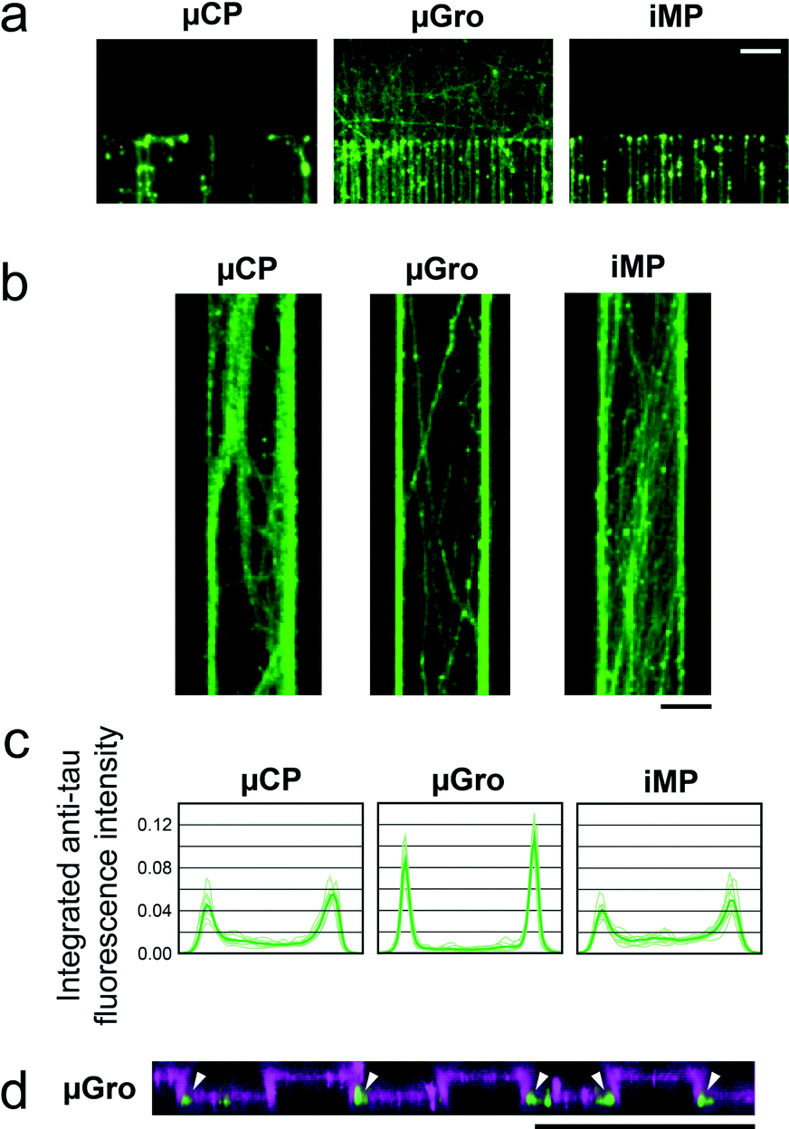 | ||
| Fig. 5 Axon behaviors at the end and within tracks. (a) Immunofluorescence of axons (green), stained by using anti-Tau antibody, at the end of the tracks on different techniques. (b) Immunofluorescence of axons (anti-Tau, green) guided on 80 μm-wide tracks in the direction from the bottom to the top of the images. (c) Normalized profiles of the integrated fluorescence intensity of axons across the tracks. Thin lines in each graph represent the profiles of 10 different samples and the thick line represents their average. (d) A projection of the cross-sectional images of PLL-FITC fluorescence (magenta) and immunofluorescence of axons (anti-Tau, green) on μGro 20 μm-wide tracks at 6 DIV, obtained from a three-dimensional reconstruction of a 18.5 μm-thick stack of 143 μm × 143 μm confocal microscopy images. The fluorescence of anti-Tau, reflecting the presence of axons, is accumulated at the corners of grooves (arrowheads). Scale bars, 50 μm. | ||
Axonal behavior inside the tracks
Axons adopt different types of trajectory according to the track widths, and most of all according to the nature of the substrate. We observed that when axons were guided on a track wider than 20 μm, i.e. a track of 40 μm or 80 μm width, the track surface was in general not totally covered by axons even at 11 DIV (Fig. 5b). A peak of the fluorescence intensity of Tau, i.e. a preferential positioning of axons along the edges of the tracks can be evidenced for the three types of guiding tracks. This phenomenon is however particularly pronounced for μGro (Fig. 5c). Confocal microscopy observation of PLL-FITC and axon immunofluorescence was performed on a fixed culture at 6 DIV on a μGro substrate, when axons are not highly bundled. The observation (Fig. 5d) revealed that axons preferably grow at the edges of the grooves on the bottom surface along the sidewalls, as indicated with arrowheads, and not on the groove walls, in agreement with a previous report.6Axon guidance from small independent populations containing several neurons by using iMP
We have shown above the interest in iMP for axonal confinement. We have further explored the potential of this hybrid constraint with the aim of compartmentalizing somas, thus dividing the seeding area into an array of small circular microchambers (Fig. 6). Different diameters, from 15 to 100 μm, were explored (data not shown). With the concentration of the cellular suspension used in this study, a diameter of 40 μm yielded a systematic filling by one cell at least, with a maximum of about 10. In this particular example, axons were guided by 5 μm-wide tracks separated by a distance of 80 μm connected to these small circular chambers (Fig. 6). Similar to what was done in larger chambers, a microfilament was placed at a distance of about 100 μm from the circles as indicated with a dotted line in Fig. 6a, and removed 1 h after cell seeding. The experiment demonstrates that the iMP technique allows a regular array of fully independent and organized neuronal compartments to be built. | ||
| Fig. 6 Axon guidance from small independent populations of neurons by using the iMP technique. (a) An immunofluorescence image of axons (anti-Tau, green), dendrites (anti-MAP2, red), and nuclei (Hoechst, blue) at 6 DIV (left) and a transmission image (right). Neurons were seeded and trapped in 40 μm-diameter circles by using the same system as the other experiments. A fishing line was placed at the distance of about 100 μm from the circles as indicated with a dashed line, and removed 1 hour after cell seeding. Axons were guided by 5 μm-wide tracks connected to the circles. (b) Transmission and immunofluorescence images corresponding to the area surrounded by rectangles in (a). Scale bars, 100 μm. | ||
Discussion
Among the three methods developed to guide axon growth in an open configuration tested here, the new approach by in-mold patterning presents strikingly superior performance, with typically 10 to 100 times less track escapes than uniformly coated microgrooves or micro-contact printing. The underlying strategy of adding chemical and physical guiding cues is thus a fruitful one. Interestingly, this difference is obtained without spectacular changes in other features of axon growth; the growth speed and the proportion of axons reaching the end of the track after 6 days are relatively similar, with a small advantage to μGro that is further discussed in ESI† text S1.Besides its superior guidance efficiency, iMP has several additional advantages over μGro and μCP. During imaging, in contrast to μCP, the position of adhesive patterns can be identified without the need for fluorescently labelled adhesive molecules that bring in a series of disadvantages: labelling may affect adhesion properties or yield some toxicity, the presence of a fluorescent background reduces the choice of fluorophores for cell imaging, and reduces the signal-to-noise ratio. Essentially, all uses of guiding patterns developed in the context of earlier guiding cues can be transposed to iMP with improved performance. For instance, neurite selection by the pattern width and shape16 is also transposable to iMP, with a stronger and longer lived confinement effect. Additionally, axons or cell bodies at the bottom of the microstructures are protected from shear stress in the microfluidic channel, if the microstructures have a significantly high aspect ratio (typically >1). Cells can be sensitive to shear stress, which can modify their phenotype or viability, and neurons are in this respect particularly fragile.36
Regarding neuron guidance, all the patterns developed within the microchannel paradigm,24–27 such as “axon diodes”,26 can be transposed to iMP, retaining the advantages of the above for neurite guidance, selectivity and/or polarization, while remaining in an open configuration.
iMP also opens new possibility for easy construction of complex, multilayer networks, out of reach of current patterning or microchannel devices. First, multilayer systems with embedded chemical patterns can be prepared much more easily than previously: the micro-pattern is visible in a simple microscope or binocular, without fluorescence. This property facilitates, during the assembly of a multilayer chip, the alignment between the substrate and features such as microfluidic channels, chambers, electrodes, etc. Since the bonding of the layers of the microfluidic chip does not occur on a plane occupied by axons, the chip can be assembled without plasma treatment and without the risk of disjoining of the two parts during growth of axons, as observed in microchannel systems in the absence of permanent bonding. The chip can thus be opened after axon growth without disturbing the neuronal array.28 Such an open configuration in turn allows direct access or addressing by chemical or physical means, such as mechanical or electrical sensing, microelectrodes, micropipettes, microlevers, patch-clamp, and the like.
“Hybrid” devices, combining guidance by iMP and fluidic insulation by microchannels, can be prepared easily, for instance by partially sealing the guiding tracks with a PDMS block with macro-chambers. This could be interesting for combining fluidic separation and axonal communication between macro-chambers, while retaining guidance in the macro-chambers. This can allow, for instance, following identical axons crossing macro-chambers containing different components, improving significantly the conventional on-chip neuron culture platforms.24–27 It is also possible to perform μCP on an iMP substrate, thus opening the route to multilayers guiding structures with overpasses and underpasses.
Finally, as demonstrated in Fig. 6, iMP can also be used for the positioning of cell somas within independent micro-chambers, with a very high selectivity. Combined with a gradient of active molecules in solution (see9 for example a combination of topographic constraints with a gradient of soluble cues), such an array of independent neuronal compartments would allow probing of independent cell responses to different concentrations of e.g. a drug on a single chip.
Regarding future possible developments, one should also remark that iMP as prepared here is patterned onto a thin layer of PDMS. Thin PDMS films without microstructures have been used in the past in stretching assays, to study mechanobiology of neurons37 or axonal injury.38 iMP structures might therefore increase the power of such studies, e.g. by imposing a predefined angle between the direction of the applied mechanical force and the direction of the axons in order to mimic some pathological situations.39 Moreover, iMP is not limited to the use of cell adhesive molecules such as PLL. For instance, carbon nanotube electrodes can be integrated into a PDMS layer by the iMP technique.40 Deformable micro-electrode arrays on a PDMS layer have also been proposed.41–43 By integrating such micro-electrodes into axon guiding tracks with high confinement efficiency, iMP could thus improve the specificity and efficiency of addressing in microelectrode array (MEA) devices.
Conclusions
In this work, we have studied the effect of three different types of cellular confinement on the growth of axons, i.e. topographical (micro-grooves), chemical (micro-contact printing), and a hybrid method combining topographical and chemical cues, called in-mold patterning. In this approach, an adhesive layer, here PLL, is deposited at the bottom of the microstructures only, leaving the walls of the structures and the upper surface non-adhesive. The potential of these different approaches for guiding and confining axons was studied using linear patterns with sizes and spacing ranging from 5 to 80 μm. Overall, in-mold patterning, applied here for the first time to neurons, provides a confinement in guiding structures 10 to 100 times higher than the two other techniques, and is also able to accurately position cell bodies in microwells. This technology was advantageously combined for initial seeding with a transient partitioning technique allowing the confinement of somas and the extension of axons in separate areas of a microfluidic chip.On the microfabrication side, in-mold patterning does not involve more complex microfabrication technologies than already needed for micro-grooves, micro-contact printing, or enclosed microchannels, or significantly longer manufacturing time as compared to μCP. The iMP technique will thus be available to numerous laboratories. It simplifies the alignment of multilayer structures with chemical micro-patterns, thus opening the route to the easy fabrication of three-dimensional arrays with overpasses and underpasses. Overall, it offers the same potential for cell positioning, confinement, and guidance as systems based on enclosed microchannels, but in an open environment giving access to a number of new experimental approaches, such as microelectrodes, micropipettes, local sensors or actuators, or chemical addressing by movable fluidic boundaries. We thus believe that it will constitute a new and important component of the growing toolbox for cell positioning, manipulation and addressing, and more generally for experimental neurosciences.
Acknowledgements
We thank Céline Braïni and the Nanofab platform in Institut Néel (Grenoble) for their help with our experiments. We thank Ivan Ferrante, Andreas Offenhäuser, Bernhard Wolfrum, Bastian Haberkorn, Philippe Tixador, Bérangère Deleglise, Anselme Perrier, and Simona Gribaudo for fruitful discussions and their technical advice. This work was performed in part in the UMR 168 microfabrication cleanroom and in the BioImaging Cell and Tissue Core Facility of the Institut Curie (PICT-IBiSA). This work was supported by ANR project Neuroscreen, grants from the European Commission: MicroDEG, ERA-NET Neuron JTC2012 “Novel Methods”, http://www.neuron-eranet.eu/en/317.php, and European research Council Advanced Grant no: 321107 “CellO”. BV acknowledges support from DGA.Notes and references
- C. Tomba and C. Villard, Microelectron. Eng., 2015, 132, 176–191 CrossRef CAS.
- Y. Xia and G. M. Whitesides, Angew. Chem., Int. Ed., 1998, 37, 550–575 CrossRef CAS.
- D. W. Branch, J. M. Corey, J. A. Weyhenmeyer, G. J. Brewer and B. C. Wheeler, Med. Biol. Eng. Comput., 1998, 36, 135–141 CAS.
- A. Offenhäusser, S. Böcker-Meffert, T. Decker, R. Helpenstein, P. Gasteier, J. Groll, M. Möller, A. Reska, S. Schäfer, P. Schulte and A. Vogt-Eisele, Soft Matter, 2007, 3, 290–298 RSC.
- T. L. Lien, J. Ban, M. Tormen, E. Migliorini, G. Grenci, A. Pozzato and V. Torre, PLoS One, 2013, 8, e73966 CAS.
- A. Beduer, I. Gonzales-Calvo, C. Vieu, I. Loubinoux and L. Vaysse, Macromol. Biosci., 2013, 13, 1546–1555 CrossRef CAS PubMed.
- J. Park, S. Kim, S. I. Park, Y. Choe, J. Li and A. Han, J. Neurosci. Methods, 2014, 221, 166–174 CrossRef PubMed.
- N. M. Dowell-Mesfin, M. A. Abdul-Karim, A. M. Turner, S. Schanz, H. G. Craighead, B. Roysam, J. N. Turner and W. Shain, J Neural Eng, 2004, 1, 78–90 CrossRef CAS PubMed.
- A. Kundu, L. Micholt, S. Friedrich, D. R. Rand, C. Bartic, D. Braeken and A. Levchenko, Lab Chip, 2013, 13, 3070–3081 RSC.
- M. J. Jang and Y. Nam, J Neural Eng, 2012, 9, 046019 CrossRef PubMed.
- E. Marconi, T. Nieus, A. Maccione, P. Valente, A. Simi, M. Messa, S. Dante, P. Baldelli, L. Berdondini and F. Benfenati, PLoS One, 2012, 7, e34648 CAS.
- J. Zhang, S. Venkataramani, H. Xu, Y. K. Song, H. K. Song, G. T. Palmore, J. Fallon and A. V. Nurmikko, Biomaterials, 2006, 27, 5734–5739 CrossRef CAS PubMed.
- S. B. N. Biancardo, H. J. Pranov and N. B. Larsen, Adv. Mater., 2008, 20, 1825–1829 CrossRef CAS.
- M. Hakanson, S. Kobel, M. P. Lutolf, M. Textor, E. Cukierman and M. Charnley, PLoS One, 2012, 7, e40141 CAS.
- S. Roth, G. Bugnicourt, M. Bisbal, S. Gory-Faure, J. Brocard and C. Villard, Small, 2012, 8, 671–675 CrossRef CAS PubMed.
- C. Tomba, C. Braini, B. Wu, N. S. Gov and C. Villard, Soft Matter, 2014, 10, 2381–2387 RSC.
- R. Fricke, P. D. Zentis, L. T. Rajappa, B. Hofmann, M. Banzet, A. Offenhausser and S. H. Meffert, Biomaterials, 2011, 32, 2070–2076 CrossRef CAS PubMed.
- H. Hardelauf, J. Sisnaiske, A. A. Taghipour-Anvari, P. Jacob, E. Drabiniok, U. Marggraf, J. P. Frimat, J. G. Hengstler, A. Neyer, C. van Thriel and J. West, Lab Chip, 2011, 11, 2763–2771 RSC.
- J. P. Frimat, J. Sisnaiske, S. Subbiah, H. Menne, P. Godoy, P. Lampen, M. Leist, J. Franzke, J. G. Hengstler, C. van Thriel and J. West, Lab Chip, 2010, 10, 701–709 RSC.
- I. Suzuki, Y. Sugio, Y. Jimbo and K. Yasuda, Lab Chip, 2005, 5, 241–247 RSC.
- W. Li, Z. Xu, J. Huang, X. Lin, R. Luo, C.-H. Chen and P. Shi, Sci. Rep., 2014, 4, 4784 Search PubMed.
- A. Kunze, M. Giugliano, A. Valero and P. Renaud, Biomaterials, 2011, 32, 2088–2098 CrossRef CAS PubMed.
- L. J. Millet and M. U. Gillette, Trends Neurosci., 2012, 35, 752–761 CrossRef CAS PubMed.
- A. M. Taylor, M. Blurton-Jones, S. W. Rhee, D. H. Cribbs, C. W. Cotman and N. L. Jeon, Nat. Methods, 2005, 2, 599–605 CrossRef CAS PubMed.
- J. W. Park, B. Vahidi, A. M. Taylor, S. W. Rhee and N. L. Jeon, Nat. Protoc., 2006, 1, 2128–2136 CrossRef CAS PubMed.
- J. M. Peyrin, B. Deleglise, L. Saias, M. Vignes, P. Gougis, S. Magnifico, S. Betuing, M. Pietri, J. Caboche, P. Vanhoutte, J. L. Viovy and B. Brugg, Lab Chip, 2011, 11, 3663–3673 RSC.
- N. D. Dinh, Y. Y. Chiang, H. Hardelauf, J. Baumann, E. Jackson, S. Waide, J. Sisnaiske, J. P. Frimat, C. van Thriel, D. Janasek, J. M. Peyrin and J. West, Lab Chip, 2013, 13, 1402–1412 RSC.
- A. Yamada, B. Venzac, I. Pereiro, S. Coscoy, M. Verhulsel, M. C. Parrini, J.-L. Viovy and S. Descroix, Submitted.
- A. C. v. Philipsborn, S. Lang, A. Bernard, J. Loeschinger, C. David, D. Lehnert, M. Bastmeyer and F. Bonhoeffer, Nat. Protoc., 2006, 1, 1322–1328 CrossRef PubMed.
- W. R. Kim, M. J. Jang, S. Joo, W. Sun and Y. Nam, Lab Chip, 2014, 14, 799–805 RSC.
- J. C. Chang, G. J. Brewer and B. C. Wheeler, Biomaterials, 2003, 24, 2863–2870 CrossRef CAS PubMed.
- T. Hamkins-Indik, S. Lam, M. E. Dueck and L. P. Lee, Chips and Tips, 17 August 2011, http://blogs.rsc.org/chipsandtips/2011/08/17/a-novel-technique-for-aligning-multiple-microfluidic-devices/ Search PubMed.
- A. Valerio, V. Ghisi, M. Dossena, C. Tonello, A. Giordano, A. Frontini, M. Ferrario, M. Pizzi, P. Spano, M. O. Carruba and E. Nisoli, J. Biol. Chem., 2006, 281, 12950–12958 CrossRef CAS PubMed.
- N. Li and A. Folch, Exp. Cell Res., 2005, 311, 307–316 CrossRef CAS PubMed.
- A. R. Kriegstein and M. A. Dichter, J. Neurosci., 1983, 3, 1634–1647 CAS.
- M. Morel, V. Shynkar, J. C. Galas, I. Dupin, C. Bouzigues, V. Studer and M. Dahan, Biophys. J., 2012, 103, 1648–1656 CrossRef CAS PubMed.
- J. Chetta, C. Kye and S. B. Shah, Cytoskeleton, 2010, 67, 650–665 CrossRef PubMed.
- B. J. Pfister, T. P. Weihs, M. Betenbaugh and G. Bao, Ann. Biomed. Eng., 2003, 31, 589–598 CrossRef PubMed.
- R. J. Cloots, J. A. van Dommelen, T. Nyberg, S. Kleiven and M. G. Geers, Biomech. Model. Mechanobiol., 2011, 10, 413–422 CrossRef CAS PubMed.
- Y. Hanein, Phys. Status Solidi B, 2010, 247, 2635–2640 CrossRef CAS.
- L. Guo, G. S. Guvanasen, X. Liu, C. Tuthill, T. R. Nichols and S. P. DeWeerth, IEEE Trans. Biomed. Circuits Syst., 2013, 7, 1–10 CrossRef PubMed.
- L. Bareket-Keren and Y. Hanein, Front. Neural Circuits, 2013, 6, 122 Search PubMed.
- S. P. Lacour, S. Benmerah, E. Tarte, J. FitzGerald, J. Serra, S. McMahon, J. Fawcett, O. Graudejus, Z. Yu and B. Morrison, 3rd, Med. Biol. Eng. Comput., 2010, 48, 945–954 Search PubMed.
Footnotes |
| † Electronic supplementary information (ESI) available: Fig. S1–S4 and text S1. See DOI: 10.1039/c6lc00414h |
| ‡ Equal contribution. |
| This journal is © The Royal Society of Chemistry 2016 |