
 Open Access Article
 This Open Access Article is licensed under a Creative Commons Attribution-Non Commercial 3.0 Unported Licence
3D printed microfluidic devices: enablers and barriers
Sidra
Waheed
ab,
Joan M.
Cabot
ab,
Niall P.
Macdonald
ab,
Trevor
Lewis
b,
Rosanne M.
Guijt
c,
Brett
Paull
ab and
Michael C.
Breadmore
*ab
aAustralian Centre for Research on Separation Sciences (ACROSS), School of Physical Sciences, University of Tasmania, Hobart, 7001, TAS, Australia. E-mail: mcb@utas.edu.au; Fax: +61 3 6226 2858; Tel: +61 3 6226 2154
bARC Centre of Excellence for Electromaterials Science (ACES), School of Physical Sciences, University of Tasmania, Hobart, 7001, TAS, Australia
cAustralian Centre for Research on Separation Sciences (ACROSS), Pharmacy School of Medicine, University of Tasmania, Hobart, 7001, TAS, Australia
First published on 25th April 2016
Abstract
3D printing has the potential to significantly change the field of microfluidics. The ability to fabricate a complete microfluidic device in a single step from a computer model has obvious attractions, but it is the ability to create truly three dimensional structures that will provide new microfluidic capability that is challenging, if not impossible to make with existing approaches. This critical review covers the current state of 3D printing for microfluidics, focusing on the four most frequently used printing approaches: inkjet (i3DP), stereolithography (SLA), two photon polymerisation (2PP) and extrusion printing (focusing on fused deposition modeling). It discusses current achievements and limitations, and opportunities for advancement to reach 3D printing's full potential.
Introduction
In recent years additive manufacturing, or 3D printing as it is more commonly known, has gained significant interest and has been spoken of as a third industrial revolution.1 Developed in the early 1980s, 3D printing converts computer-assisted design (CAD) into a physical object in a single process (Fig. 1).2 It remained a technology with relatively restricted use until the expiration of a key patent in 2009, but since then there has been a significant increase within the manufacturing industry as well the consumer market because of the ability to easily create unique bespoke one-off objects.3 The market for additive manufacturing has grown by 35.2% to $4.1 billion in 2014 and is expected to become a $20.2 billion global industry by the end of the decade.4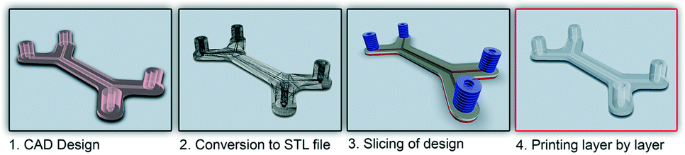 | ||
| Fig. 1 The additive manufacturing process. The CAD file is converted into a standard triangulation language (STL) file. The STL file is digitally sliced into individual layers that are sequentially realised to build an object in a layer-by-layer manner. | ||
Commercial 3D printers capable of producing structures ranging from few microns to several centimetres are beginning to challenge soft lithography as the research prototyping approach to micro-fabrication. The significance of PDMS and soft-lithography to the microfluidic community is high as it enabled a new generation of researchers to undertake research in the field due to the low infrastructure costs and ease of manufacture.5 However, it has many limitations, including the material properties of PDMS and the fact that this material does not translate well to a commercial scale. Nor are the properties similar to mass-production manufacturing, such as etching (glass and silicon) or embossing and injection moulding (thermoplastics).6,7 Furthermore, all of these fabrication approaches are limited by the range of features that can be created, with a move from 2.5D (structures with varying width but identical depth) to 3D structures significantly increasing processing cost and reducing success rates.
The attraction of 3D printers is twofold. First is the unprecedented ability to fabricate in three dimensions in a way that has not been previously possible. This presents new opportunities in the field of microfluidics as researchers begin to imagine what might be possible when manipulating surfaces and fluids in three dimensions. The second feature – the ability to rapidly realise a model – enables researchers to adopt a “fail fast and often” strategy. A simple cross fluidic microchip can be printed in 10–15 min, while more complex ones may take hours. This is in a material that is more similar to thermoplastics than PDMS (and with some printers, may actually be the same thermopolymer) suggesting translation into commercial outcomes may be simpler.
Despite of all these benefits, 3D printed structures cannot currently compete with the resolution of structures produced by conventional lithography in a build space that is useful. There are also concerns regarding dimensional fidelity, shape conformity, surface quality, biocompatibility, optical transparency and material availability.
To date, Waldbaur et al.8 and Vaezi et al.9 have reviewed technical aspects of all current 3D printing technologies, including other approaches that have had some preliminary reports on printing microfluidic devices (such as selective laser sintering).10 Recently, Au et al. published a comprehensive review highlighting the impact of 3D printing in the field of microfluidics.11
This review focuses on progress made towards the use of 3D printing for the fabrication of polymer microfluidic devices. Suitable approaches that have been used successfully include inkjet 3D printing (i3DP), fused deposition modelling (FDM), stereolithography (SLA) and two photon polymerisation (2PP). A practical overview of the range of materials that can be processed and the parameters influencing printing performance are listed together with the printing accuracies realised for various printers. This present review discusses how the current state of the art for 3D printing has fabricated microfluidic devices for various applications, where the barriers reside and how the technology can develop into achieving its full potential.
Inkjet 3D printing (i3DP)
Fundamentals of i3DP
The i3DP process is based on inkjet technology which either operates in continuous or drop on demand (DoD) mode.12 Continuous mode operates with ink of a lower viscosity with higher drop velocity than DoD.13 The DoD mode is the method of choice for 3D microfibrication as it generates smaller droplets with higher placement accuracy which should translate to finer and more repeatable microfluidic structures.14 In the DoD technique, a pulse is generated either thermally or piezoelectrically as shown in Fig. 2. In a thermal DoD, ink is heated locally to form vapour bubbles that eject as an ink droplet. In piezoelectric DoD, acoustic pulses, generated by the deformation of piezoelectric element, push the droplet of ink from the nozzle. Piezoelectric DoD is suited to variety of solvents whereas in thermal DoD solvent must be volatile.15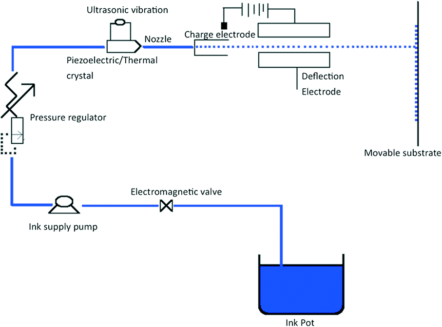 | ||
| Fig. 2 Schematic illustration of DoD printing process. | ||
There are four critical elements for the high accuracy performance of inkjet printing as shown in Fig. 3. Each element involves different technical considerations, which have been discussed in detail by Chen.16
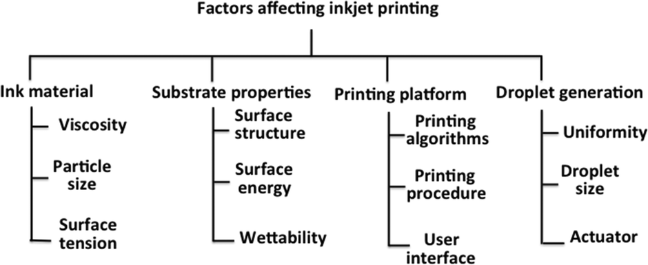 | ||
| Fig. 3 Key factors affecting inkjet process. | ||
i3DP can be further divided into two categories: powder-based and photopolymer based. In powder-based i3DP, solid powder particles are bonded with polymeric adhesive solution delivered by an inkjet print head. The process begins with the deposition of a layer of powder spread uniformly on the building stage by a roller. The multi-channel printer head sprays droplets of adhesive onto the powder bed at the targeted area. After the first layer is completed, the building platform drops and second powder layer is distributed and bound by the next layer of adhesive. This process is repeated slice after slice until 3D object is formed (Fig. 4).17 The loose supporting powder surrounding the printed object can easily be brushed away (except from a fully enclosed structure where the powder remains) and does not require any significant post-processing step. The unused powder is continuously recycled which lowers the costs of printed objects. The powders are a combination of gypsum, polymer and silica particles with adhesives that are composed of glycerol and water-soluble acrylates. The powder size is approximately 50–100 μm, and with 2–4 particles forming a layer the Z-resolution is limited to 200 μm. The particle size, shape and packing density determine the resolution of the printers.18 The non-bound particles can increase the surface roughness and reduce the transparency of printed object because of light scattering by the particles in the bulk, hindering microscopy studies desirable for many microfluidic applications.19
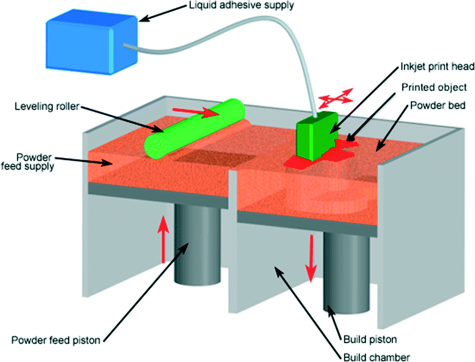 | ||
| Fig. 4 Powder inkjet printing process: the roller spreads powder over the bed, with the excess powder providing a support to the printing object. Photopolymerisable ink is then deposited onto the powder to bind the particles together.20 (Copyright 2008 Custom Part Net). | ||
Photopolymer based inkjet printers use an array of inkjet print heads to deposit tiny drops of the build- and support-material to form the object in a layer-by-layer fashion. The build material is typically an acrylate-based photopolymer and includes monomers, oligomers, and a photo-initiator to cure each layer with a UV source (Fig. 5). Despite being limited to photopolymers there are over 100 commercial composite materials available based on 17 primary photopolymers. The multi-material printing allows up to 14 materials to be printed simultaneously on the same tray with a wide range of physical properties, including color and surface morphology. The composite material includes varying ratios of acrylonitrile butadiene styrene (ABS), polystyrene (PS), polypropylene (PP), polymethylmethacrylate (PMMA), polycarbonate (PC), ethylene propylene diene monomer (EPDM) and high impact polystryrene (HIPS).21
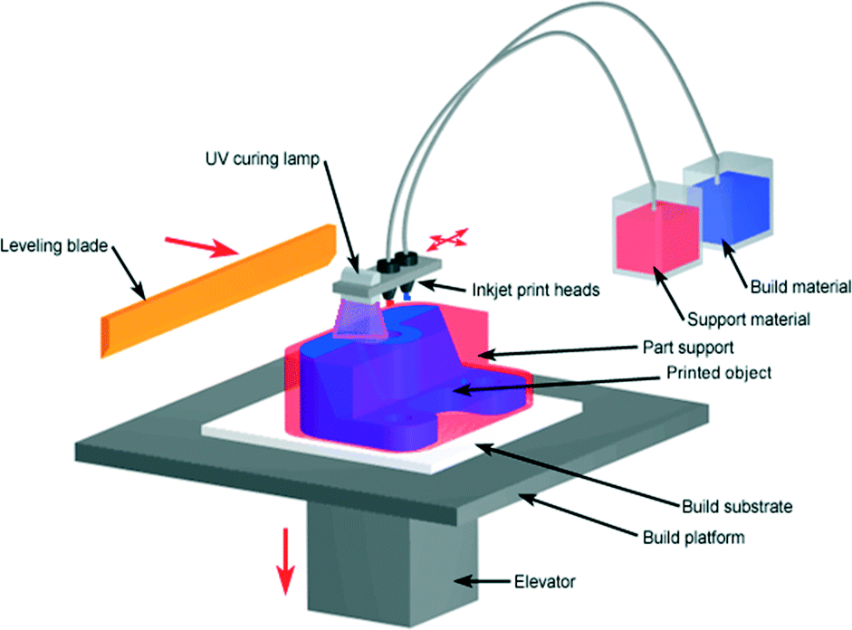 | ||
| Fig. 5 Photopolymer based inkjet printer.20 (Copyright 2008 Custom Part Net). | ||
Commercial manufacturers, such as Objet Geometries Ltd and Stratasys use DoD technology, termed poly jet modelling (PJM), while 3D Systems use multijet modelling (MJM). In both cases, the print head has many small holes that jets droplets of build material and support material simultaneously, to build 3D structure.
In PJM, the support structure is a mixture of propylene, polyethylene, acrylic monomer and glycerin. This can be removed by high pressure water jetting followed by washing in a chemical bath (2% NaOH) to remove residue of support material. High pressure water jetting may damage delicate parts. With MJM, the support material is made up of paraffin wax and is removed using heat to melt the paraffin, with additional steps, like soaking in an ultrasonic bath of oil to remove wax from crevices, performed if required. One of the major impediments to the use i3DP for microfluidics is the need to remove the support material, which is impossible for fully enclosed structures and difficult through narrow channels. The clogging of holes in a print head due to dry ink reduces the performance efficiency of the printer and thus, to maintain good performance, i3DP needs to be used regularly. There is also considerable cost (up to several hundred dollars) in changing from one material to another as the system needs to be flushed with the new propriety material.
Bonyár et al. moved closer to this ideal by directly printing 1000 × 2000 μm open microchannels using an Eden 250 inkjet system.23 The microgrooves were then sealed with a thin transparent foil to create a sealed microchannel. Whilst this streamlined the process by directly printing the channels, sealing adds an additional step involving a different material. It must also be noted that the feature size of the microchannels is significantly larger than is commonly used in the field.
In subsequent work, Bonyár et al. critically compared the printing accuracy and quality of the matt and glossy printing modes of the Objet Geometries Eden 250 3D inkjet printer.24 Test pieces were designed with 6 structural zones. The dimensional series were categorised into two groups: one with dimensions that were an even integer multiple ranging from 2 to 8 of the printers X, Y, Z resolution (42, 84, 16 μm) and the second an even integer multiple (2–8) of 50, 80 and 20 μm. More accurate prints were obtained when the channel depth was designed as an integer multiple of the Z-resolution (16 μm). The average deviation from theoretical depth value was 7.3% for the matt mode and 9.9% for the glossy mode, with even multiple integer of Z-resolution. In glossy mode, the minimum channel width was 400 μm due to sagging of the walls as a result of the absence of support material, with a high average deviation from the theoretical width value of 33.5% in X and 51.2% in Y for channels with a width above 250 μm. In matt mode, deformation was observed for dimensions above 150 μm for the Y direction (13.9% error) and for the X direction (18.7% error), with the minimum channel width of 200 μm. It was concluded that matt mode was more suitable for microfluidic purposes because of its higher accuracy and resolution, but glossy printing provided better transparency.
Walczak et al. compared dimensional fidelity, shape conformity and surface roughness of open and embedded rectangular and semi circular microchannels printed using four different inkjet printers (two Stratasys printers and two 3D System printers).25 The minimum dimension for printed microfluidic channels was approximately 200 μm, with smaller structures not printed or deformed. Generally, less deformation was observed in structures printed by 3D Systems, and deformation was more prominent along the x-axis than in the y-axis. Significant deformation was observed in Stratasys printers working in glossy mode. Moreover, Stratasys devices were blocked by support material, as the water jet could not penetrate into microchannels. The surface roughness of the structures printed by 3D Systems was 0.38–0.61 μm. This is slightly poorer than micromilling26 and much poorer in comparison to 2PP (4–11 nm),27 though better than 3.24–42.9 μm reported by FDM.28 Only the highest nominal resolution printer (ProJet 3000 HD+) had identical surface roughness values in both horizontal and vertical printing direction, due to a specifically constructed printer head and reflow of support material. For the other printers surface roughness was almost double when printing vertically. The source of print error in the inkjet printers was related with volume and deposition mechanism of a droplet. The authors proposed a simple method of correction for this error, which decreased the difference between designed and real dimensions to less than 5%.
Hwang et al. printed periodic pillars with constant diameter of 250 μm with variable pitch (Fig. 6(A–F)).29 They found the resolution of the printer depended on the droplet size, printer nozzle spacing and reflow of material prior to UV curing. These factors affected the droplet spreading which ultimately changed the final dimensions of printed devices.
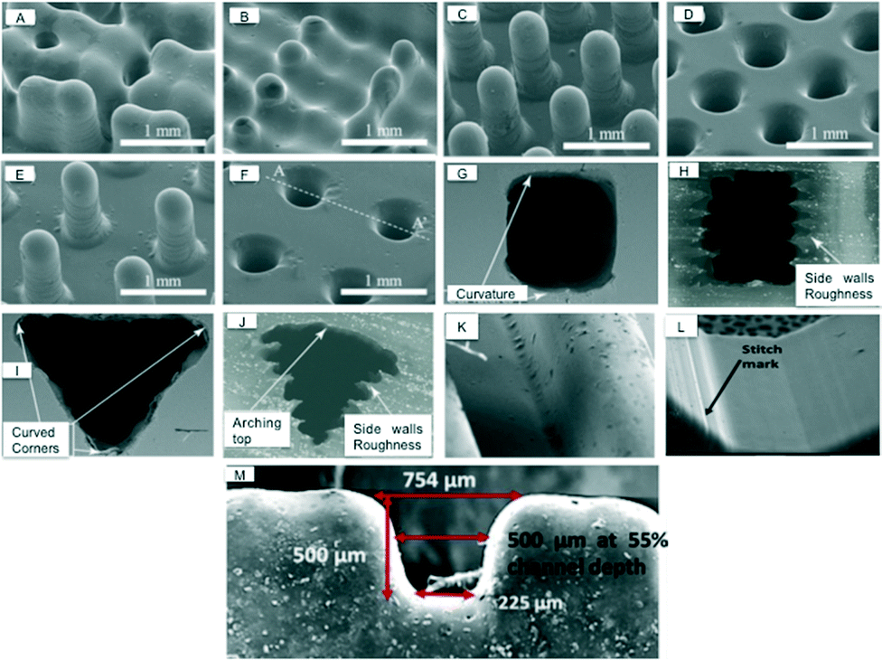 | ||
| Fig. 6 Scanning electron micrograph (SEM) of channels printed by different inkjet printers. (A–F) Pillars with 250 μm diameters and 1500 μm heights were printed (A), (C) and (E) and imprinted in PDMS (B), (D) and (F). The pitch was (A–B) 500 μm, (C–D) 750 μm and (E–F) 1000 μm. The final printed pillar diameters were 378 μm, resulting in structures with multiple pillars bleeding into one another when the pitch was not large enough (A–B).29 (Copyright 2015 Elsevier) (G) Cross-section of the vertically and (H) horizontally printed rectangular microchannels. (I) Cross-section of the vertically and (J) horizontally printed trapezoidal microchannels. The vertical 3D printed channel produced good shape conformity while the inferior shape conformity of horizontal channels was due to side wall roughness.30 (Copyright 2015 IOP Publishing) (K–L) The stitch marks increased surface roughness. (M) Distribution of width within printed channels (500 × 500) μm due to leaning walls.28 (Copyright 2015 Springer). | ||
Connor et al. quantified a dimensional fidelity and precision of embedded channels using ProJet HD 3500 inkjet printer.30 Rectangular and trapezoidal channel arrays were printed in the vertical (perpendicular to XY-axis) and horizontal directions (parallel to XY-axis), to determine the influence of print orientation. The vertical 3D printed channel produced good shape conformity when compared to horizontal printing approach as shown in Fig. 6(G–J). The inferior shape conformity of horizontal channels was due to side wall roughness. They concluded that for microfluidics, vertically 3D-printed channels yield better shape conformity and dimensional fidelity with variances from two to four times larger than conventional deep reactive ion etching (DRIE) techniques, but the significance of the individual layers along the length of the microchannel and the associated roughness was not discussed.
Lee et al. evaluated microfluidic features using an Objet Eden 350 V printer and found an average deviation of 25.2 μm between actual and printed diameter.28 The surface roughness was increased with increased side wall angle due to the formation of stitch marks, as shown in Fig. 6(L). The surface roughness ranged between 0.47 to 8.44 μm for angles between 0° to 60° and at 90° the roughness decreased to 1.7 μm. The Fullcure 720 built material was found to be hydrophilic in nature, having a contact angle of 81.0°.
Lee et al. determined the operating range of ProJet HD 3500 printer, by printing open microchannels of 100–1000 μm in width and 50–500 μm in height.31 It was observed that channels with less than 100 μm width and 50 μm height collapsed. The microchannel width varied by ∼35 μm between the CAD and printed device and the height difference was less than 11 μm. They also concluded that better accuracy was obtained when printing in a vertical direction.
Gowers et al. printed microfluidic devices using two different 3D printers.32 First, a microfluidic chip was fabricated using an ULTRA 3SP printer and ABS 3SP resin – a white build material that allows printing of dimensionally and mechanically stable components. The set of three channels having variable dimensions of (i) 520 × 520 μm (ii) 750 × 550 μm (iii) 1000 × 550 μm were printed. However, the printed device had almost 100 μm smaller dimensions than those specified in the design. This decrease was attributed to shrinkage of material during printing process. Objet260 Connex printer was used to print needle holders. The main advantage of using this printer compared to the ULTRA 3SP is the possibility to print rigid and soft material simultaneously on the same component. VeroWhitePlus (RGD835) and TangoBlack (FLX973) were employed for the printing of the rigid and soft parts, respectively. The 3D printed microfluidic device coupled with novel 3D printed holders incorporates removable needle type integrated biosensors, for glucose and lactate detection.
Paydar et al. explored multi-material 3D printing for microfluidic interconnects.33 They fabricated an interconnect consisting of a flexible elastomer (Tangoblack) O-ring co-printed with rigid plastic (VeroBlack) barbed clips for mechanical clamping onto a microfluidic chip. The clamp and gasket were printed in a single step, eliminating the need for adhesives and additional assembly. The low manufacturing cost made this interconnect a competitive alternative to other available interconnect technology. The interconnect tolerated a sealing pressure up to 416 kPa. However subsequent tests with similar interconnect had a lower maximum sealing pressure due to material fatigue. Breakage of the interconnect under stress was observed due to grains deposited during printing. Robustness of the interconnect could be increased by avoiding grains along the axes of stress concentration.
Sochol et al. used MJM approach for the design and construction of integrated microfluidic circuits (IFC) including diodes, capacitors and transistors.34 The smallest dimension of fluidic circuit was 200 μm and minimum fluidic component thickness was 150 μm. The 3D printed IFC exhibited operational characteristics consistent with their electrical analogues, both independently and as part of integrated networks. By modifying geometric parameters of the 3D fluidic components, one can readily customise core component functionalities. In addition, the 3D component models can be assembled as desired to achieve a diverse array of integrated fluidic processors and networks.
Coating 3D printed channels with polydimethylsiloxane (PDMS) and polystyrene (PS) was used by the Spence group to overcome the limitation of unknown surface chemistry of proprietary resin and also to make it transparent and amenable to cell adhesion.35 The printed channels were at the millimeter scale and therefore support material was easily removed, but it was difficult to remove support material for channels with dimensions less than 500 μm.36 Using successive coatings of PDMS or PS, the microchannel dimensions were reduced to 100 μm, which is an elegant and functional way to improve the channel size from 3D printing, although it requires additional steps.
Macdonald et al. investigated the biocompatibility of inkjet resin (VisiJet Crystal EX200) against zebrafish embryo.37 This resin is categorised as a class VI certified material by United States Pharmacopeia (USP) for plastic biocompatibility. The result revealed that the untreated commercial resin was incompatible for the growth of zebrafish embryos. However, biocompatibility was improved by treating it with ethanol. Similar results were found for Fullcure 720 build material which was declared to have similar biocompatibility when treated with ethanol.28
i3DP capabilities have been showcased by making devices with different microfluidic functionality by a number of groups, which has been mentioned in Table 1.
| Printing technology | Model (manufacturer) | Material | Resolution (x, y, z) μm | Advantages reported | Disadvantages reported | Application |
|---|---|---|---|---|---|---|
| a Resolution in 2PP is very high compared with the other 3D printer techniques explained here (<1 μm). Resolution of the printer is normally not reported. b XY resolution was based on the nozzle diameter of the FDM printers. M.O. mail order; n.r. not reported. | ||||||
| Inkjet 3D printing (i3DP) | ||||||
| MJM (3D Systems) | ProJet 3500 HD | Acrylonitrile | 39 × 39 × 29 | Vertically printed channels have dimensional stability and smooth surface | Features printed along Y-axis show rough surfaces and low dimensional accuracy | Study of printing performance for microfluidic features30 |
| 39 × 39 × 16 | Solve alignment problem and cost effective | n.r. | Droplet production through T-junction123 | |||
| ProJet 3500 HDPlus | VisiJet Crystal | 50 × 50 × 32 | Repeatable production of models for biocompatibility studies with zebrafish | Photopolymers are not biocompatible with fish embryo test | Evaluation of biocompatibility of inkjet, SLA and FDM 3D printers37 | |
| VisiJet S300 | 25 × 25 × 29 | |||||
| VisiJet M3 Crystal | 34 × 34 × 16 | Module like assembly, Recyclable, easy access for non-expect user | Channels less than 100 μm in width and 50 μm cannot be printed. | Fabrication of liver cancer diagnostic device31 | ||
| ProJet 3000 HD | VisiJet M3 Crystal | 38 × 38 × 32 | Modular approach. Fluidic components for static and dynamic physical elements. Develop integrated microfluidic circuits. | Observed residual flow through closed interactions. Material exhibits limited optical characteristics and biocompatibility. | Fabrication of fluidic circuit components including capacitors, diodes and transistors34 | |
| ProJet 3000 HD+ | VisiJet M3 polymer | 38 × 38 × 16 | Better nominal resolution and accuracy achieved. Identical surface roughness in both axis. No manual work is required to remove support material for printer. 200 μm open channels achieved | Deformation is prominent while printing in X-axis. Microchannels slightly smaller. | Evaluation of printing performance of four inkjet printer for microfluidic features25 | |
| ProJet 3510 HD | ABS | 68 × 68 × 32 | Reusable, reduce waste, reduced set-up time | n.r. | Micro-capillary device for double emulsion generation124 | |
| ProJet 3510 SD | VisiJet M3 polymer | 67 × 67 × 32 | Better nominal resolution and accuracy achieved. No manual work is required to remove support material for printer. 200 μm open channels achieved | Deformation is prominent while printing in X-axis. Microchannels slightly smaller. | Evaluation of printing performance of four inkjet printer for microfluidic features25 | |
| ThermoJet | ThermoJet 2000 | 85 × 64 × 42 | Rapid process, Multi-level features, Non-toxic | Channels below 250 μm were not achieved and surface roughness effect optical performance | Fabrication of molds and microfluidic mixers22 | |
| PJM (Stratasys) | Objet24 | VeroWhitePlus RGD-835 | 42 × 42 × 28 | 200 μm open channels achieved | Deformation is prominent while printing in X-axis. The surface roughness of parallel and perpendicular directions was almost double. Default printing patter. Microchannels slightly bigger. | Evaluation of printing performance of four inkjet printer for microfluidic features25 |
| Easy fabrication of multi-level and helical molds | Limitation in printing resolution | Fabrication of complex microfluidics molds29 | ||||
| Objet30 Pro | VeroWhitePlus RGD-835 | 42 × 42 × 16 | Lower surface roughness founded than other i3DP tested when printed in glossy mode. 200 μm open channels achieved | Deformation is prominent while printing in X-axis. The surface roughness of parallel and perpendicular directions was almost double. Microchannels slightly bigger. Significant shape deformations when working in glossy mode. | Evaluation of printing performance of four inkjet printer for microfluidic features25 | |
| Objet Eden350V | FullCure 720 | 42 × 42 × 16 | Biocompatibility increases with treatment with ethanol | Surface roughness varies with printing angle for i3DP | Evaluation of printing performance for microfluidic features28 | |
| Objet Eden250 | FullCure 720 | 42 × 82 × 16 | Matt mode is more accurate, Glossy mode give transparency | Glossy mode showed high deviation from designed dimensions | Study of printing accuracy of two modes for microfluidic device24 | |
| Direct printing of microfluidic prototypes, Cost effective process | Sealing of device makes it multistep process | Storage of gynaecological cervical sample23 | ||||
| Objet Connex 350 | VeroClear | 42 × 42 × 16 | Modular device | Difficulty in removing support material | Study of drug transport, cell viability and electrochemical sensing36 | |
| Rugged, robust, reusable, user friendly device | Difficulty in removing support material below 250 μm | Study of electrical cell lysis in polymer coated 3D printed devices35 | ||||
| Modular device | Difficulty in removing support material below 250 μm | Electrochemical detection of ATP and RBC purification in integrated microfluidics devices125 | ||||
| VeroWhitePlus | 42 × 42 × 16 | Biocompatible, Reusable, modular device | n.r. | Study of drug transport and cell viability126 | ||
| Objet260 Connex | TangoBlack FLX973 | 42 × 42 × 16 | Modular device. Possibility to print rigid and soft material simultaneously on the same component | n.r. | Microfluidic device for subcutaneous monitoring of tissue glucose and lactate32 | |
| VeroWhitePlus RGD-835 | ||||||
| n.r. (Quickparts M.O.) | TangoBlack | n.r. | Multi-material fabrication of low cost interconnects | Printing services do not mention model number of printer | Fabrication of interconnects for microfluidics33 | |
| VeroBlack | ||||||
| 3SP (scan, spin and selectively photocure) | ||||||
| EnvisionTEC ULTRA 3SP | ABS 3SP White | 100 × 100 × 25 | Modular device. Easily removable partially cured perforated supports and a single material is used for both build and support | Limitation in printing resolution | Microfluidic device for subcutaneous monitoring of tissue glucose and lactate32 | |
| Stereolithography (SLA) | ||||||
| DP-SLA | Miicraft | Acrylate based resin | 56 × 56 × 50 | Low cost and transparent microfluidic chip | Improvement in resin property and hardware is required | Development of mixer, gradient generation, Droplet extraction and determination of nitrate in tapwater53 |
| Accept 40% methanol water mixtures and pH between 2–10 at concentration of 50 mM | n.r. | Achieve mixing from 4 channels for acid/base reactions and methanol water mixtures127 | ||||
| Modification in resin and cost effective process | n.r. | Tunable surface properties62 | ||||
| Multi-level sealed channels with varying thickness from 50 to 500 μm were achieved | Coating of template is required | Fabrication of template, Determination of micromixer performance and glucose sensing50 | ||||
| Direct printing of multi-level microfluidic chip | n.r. | Determination of H2O2 and glucose sensing52 | ||||
| Rapid, cost effective process | Limitation in resolution, post treatment is required | Fabrication of chaotic advective mixer, peristaltic valve and injection on demand microfluidic devices51 | ||||
| Sensitive method | n.r. | Fabrication of solid phase extraction preconcentrator for selective extraction of trace elements and removal of unwanted salt55 | ||||
| Autonomous LOC sensing on cell phones. Possibility to operate on cell phones of diverse brands | Quantitative glucose detection via 3D printed, disposable unibody LOC, configured on cell phone59 | |||||
| B9Creator 3D printer v1.1 | Modified resin (Irgacure 819 and Sudan I) | 50 × 50 × 50 | Horizontal channels with 350 × 250 μm were 100% accurate | Modification in resin caused bulk fluorescence | Fabrication of microfluidic device with valves56 | |
| n.r. (Shapeways Frosted Ultra Detail M.O.) | Clear acrylic polymer | 100 × 100 × 50 | Cost effective, fast delivery, inexpensive and clear photoactive resin. | Limitation in printing resolution. | Golden gate DNA assembly in 3D microfluidics. Co-laminar mixer61 | |
| UV-LED | PicoPlus 27 (Asiga) | PlasCLEAR | 27 × 27 × 0.25 | Simple, accuracy, biocompatible | n.r. | Microfluidic chip coupled with light addressable potentiometric sensor was printed for cell culturing54 |
| PlasCLEAR | 27 × 27 × 1 | Higher resolution. Microfluidic channels with less than 100 μm can be printed | n.r. | Formulation of a new resin for 3D printing microfluidic channels. Comparison with other commercial resins66 | ||
| FSL Clear | ||||||
| PR48 | ||||||
| Modified resin (PEGDA, Irgacure 819, Sudan I) | ||||||
| Laser | Viper SL System (3D Systems) | Water-Shed XC11122 | 100 × 100 × 50 | Low cost, biocompatible skill-less technique | Limitation in resolution, and post treatment is required to decrease surface roughness and increase optical clarity | Evaluation of printing performance of SLA printer60 |
| User friendly, low cost, biocompatible | Limited printing resolution, Performance of valve was inferior than traditional PDMS | Integration of microfluidic chip via 3D printed valves and pumps57 | ||||
| Effective detection of pathogen | n.r. | Detection of pathogenic bacteria in food sample128 | ||||
| Viper pro (3D Systems) | WaterShed 11122XC | 25 × 25 × 50 | Post treatment process make Fototec SLA 7150 more biocompatible | Resins are not biocompatible with fish embryo test | Evaluation of biocompatibility of inkjet, SLA and FDM 3D printers37 | |
| Dreve Fototec 7150 clear | ||||||
| Agilista-3000 | AR-M2 | 39 × 61 × 15 | Effective as a mold for rapid production of PDMS microfluidic chips | Lack printing accuracy | Study of concentration gradient of soluble factors within PDMS microfluidic channels and their effect on human cell129 | |
| Form1+ | Clear photopolymer (FLGPCL02) | 300 × 300 × 25 | Cost effective, rapid fabrication and clear photoactive resin. | Limitation in printing resolution. | Golden gate DNA assembly in 3D microfluidics. Co-laminar mixer and 3D micromixer61 | |
| n.r. (FineLine Prototyping M.O.) | Somos WaterShed 11122 XC | n.r. | Modular and reconfigurable fluidic components | n.r. | A sample library of standardised microfluidic component and connector67 | |
| EnVisionTEC (180 W Hg Lamp) | Own formulation (PDMS based) | 30 × 30 × 100 | Orange dye increases resolution. Effective direct printing of gas permeable PDMS membranes. | Optical clarity is sacrificed | PDMS CO2 permeable membrane65 | |
| Two-photon polymerisation (2PP)a | ||||||
| Femtosecond Laser | Ti:sapphire laser (Coherent Mira 900-F) | Modified resin (SU-8 2150 based) | n.r. | Fabrication speed was increased from 200 μm s−1 to 1 cm s−1 | Preparation of resin is time consuming | Fabrication of template86 |
| Ti:sapphire laser (Kapteyn-Murnane Laboratories Inc., CO) | SU-8 2025, negative photoresist | n.r. | Fabrication time was 45 min | Time consuming process for the complicated structures | Fabrication of template for trapping yeast cell87 | |
| n.r. | SU-8 negative photoresist | n.r. | Does not require mask | n.r. | Fabrication of mirochannel88 | |
| n.r. | Modified positive photoresist | n.r. | Hollow microstructure occupies small portion of microfluidic chip | Positive resist involve subtractive type of fabrication | Fabrication of mirochannel89 | |
| n.r. | SU-8 negative photoresist, NOA 61 | n.r. | Surface profile scanning reduces fabrication time | Not effective for thin and porous structure, Additional UV exposure is required | Fabrication of free standing and mechanical microvalves, levers, nanoshell90 | |
| n.r. | PDMS | n.r | High resolution microfluidic structure | n.r. | Fabrication of microchannels91 | |
| Fused deposition modelling (FDM)b | ||||||
| Extrusion | Fab@Home Version 0.24 RC6 freeform | Acetoxysilicone polymer (LOCTITE 5366) | n.r. | Reusable, inbuilt and self-healing bespoke reactionware. Low-cost, reconfigurable and highly accessible format | Poor resolution | Fabrication of reactionware for organic synthesis and analysis111 |
| 3DTouch | Polypropylene | 125 × 125 × 200 | Inert and low cost material, time and cost-effectiveness | Suitable for 3D-printed milli-devices. Blockage may occur due to formation of precipitate | Miniaturised fluidic reactionware fabrication for chemical syntheses112 | |
| Dimension Elite | ABSplus-P430 | 178 × 178 × 178 | Biocompatibility increases with treatment with ethanol | High surface roughness for FDM | Evaluation of printing performance for microfluidic features28 | |
| Dimension SST 768 | ABS-P400 | 254 × 254 × 254 | Variable widths were achieved in single device at low cost | Surface roughness effect laminar flow, Choice of polymer is limited | Characterisation of capillary valves in centrifugal microfluidics devices114 | |
| n.r. (modified desktop 3D printer) | Sugars PDMS | 100 × 100 × n.r. | Biocompatible, cost effective microfluidic devices with acceptable printing accuracy | Nozzle blockage may happen with sugar purity lower than 95%. | 3D sugar printing of microfluidic chip116 | |
| MakerBot Replicator 2X | PLA | 400 × 400 × 200 | Low cost and portable device | Detection limits are lower, sequential task must be completed by operator | Electrochemiluminescent immunoassay for the detection of cancer biomarker proteins117 | |
| PET ABS | 400 × 400 × 200 | Reusable, mechanically stable devices with reproducible detections | Semi-transparent devices | Low cost 3D-printed fluidic mixer for H2O2 sensing via flow-injection amperometry using Prussian blue nanoparticles119 | ||
| Easy3DMaker | PLA | 100 × 100 × 80 | Rapid, sensitive, specific detection of influenza virus | Optimization steps needed | Electrochemical detection of influenza hemagglutinin for infectious diseases121 | |
| Profi3Dmaker | ABS | 100 × 100 × 80 | Rapid and sensitive detection of pathogens | n.r. | Detection of pathogens in food120 | |
| Airwolf3D HD2x | PLA | 350 × 350 × 60 | Low cost versatile mixers | n.r. | Different mixer channel were designed, coupled with three different spectroscopic pro be118 | |
However in order to truly penetrate the microfluidic field there remain a number of significant challenges. At present, i3DP can work with over 100 different raw materials. This is insignificant when compared with the enormous range of raw materials used in traditional manufacturing. Transparent and highly biocompatible materials are required for application in biomedical devices. New support materials with different removal processes are necessary if fully enclosed microchannels in the 10–100 μm range are to be printed. Promising steps for optimisation of droplet formation and reflow of drops prior to UV curing are also required. This must be accompanied by an increase in resolution in both XY and Z planes in order to realise this, which will likely come at the expense of build space and print time.
Stereolithography
Fundamentals of SLA printing
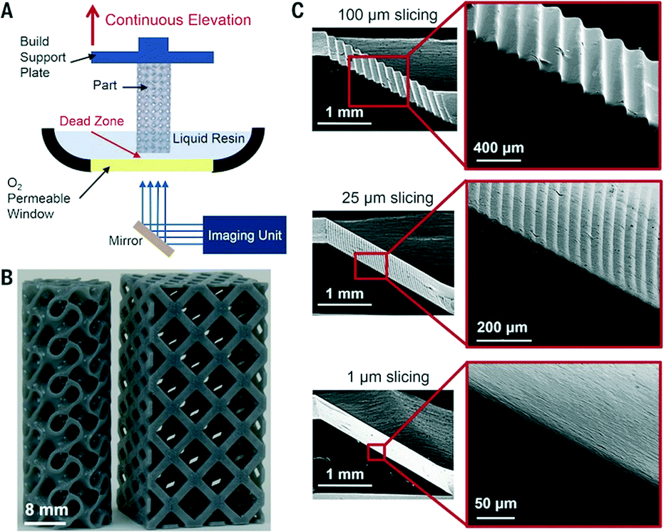
Stereolithography (SLA) was developed by Chuck Hull in 1986 and commercialised at 3D Systems in 1988.2 He defined it as “a method and apparatus for making solid objects by successively “printing” thin layers of a curable material, e.g., a UV curable material, one on top of the other”. There are two important configurations: free surface approach (bath configuration) and constrained surface approach (bat configuration).38In both configurations objects are built in a layer-by-layer manner by spatially controlled photopolymerisation of a liquid resin which is performed with either a scanning laser or a digital light projector (DLP).39 The bath configuration is the classical setup for SLA in which a UV beam traces a 2D cross section onto a substrate submerged in a tank of photoactive resin that polymerises upon illumination as shown in Fig. 7A. After completion of the 2D cross section, the substrate is lowered further into the resin by a predefined distance, and the UV beam begins the addition of the next layer, which is polymerised on top of the previous layer. In between layers, a blade loaded with resin levels the surface of the resin to ensure a uniform layer of liquid prior to another round of UV light exposure. In this configuration the height of the printed object is restricted to the tank size. Chemical reactions with ambient air, resin waste and extensive cleaning procedures are serious concern of bottom-up approach.
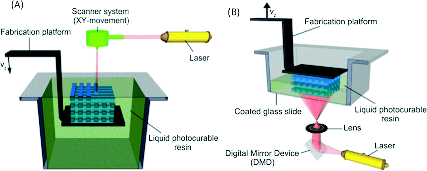 | ||
| Fig. 7 Two SLA printing configurations. (A) Laser-scanning SL with the free surface/bath configuration. (B) DLP SLA with the constrained-surface/“bat” configuration.43 (Copyright 2015 Elsevier). | ||
The constrained surface approach is also called ‘bat’ configuration due to the fact that the object is created hanging from the movable substrate like a bat from a ceiling as shown in Fig. 7B. The movable substrate is suspended above the resin reservoir. The light source is located beneath the tank which has an optically clear bottom, and a non-stick layer so that the printed structure does not adhere to the substrate. The constrained surface approach has several advantages over the bath systems and is increasingly being applied in stereolithography.40 The surface of resin being illuminated is smoothed and refreshed through gravity and by letting the surface rest over a given settling time. Only small amounts of resin with low viscosity are required as the object is pulled out of the resin, rather then submersed in it. The illuminated layer is not exposed to the atmosphere, so oxygen inhibition is limited. The height of printed object is not restricted and it requires minimum cleaning steps as compared to bath configuration.39,41 However, a cured layer is sandwiched between the previous layer and the resin vat. The solidified material may adhere strongly to the bottom of vat causing the object to break or deform when the build platform moves up from the vat during the building process.42
Exposure with a DLP has emerged as a promising source for illuminating the resin. A digital mirror device (DMD) with an array of several million mirrors is used and is essentially a digital projector modified to only emit UV light. The attraction in using a DLP is that by projecting a 2D pixel-pattern onto resin, a complete layer of resin can be cured at the same time. This means that build times are quicker when compared to a rastering laser, as they only depend on the layer thickness and on the required exposure time, and not the XY build size of the model.44 They are also mechanically simpler, only requiring accurate Z-control and a number of low cost printers (<$5000) have been released by various manufacturers.
Waldbaur et al. established a DLP lithography system coupled to a high-pressure mercury lamp equipped with custom-made demagnifying projection optics.45 The projection optics consisted of thousands of individually addressable micro mirrors which can be tilted to an on- or off-state. In order to have maximum flexibility the system was equipped with high-pressure mercury lamp as the light source, filtered to the required wavelength. This technique illuminates an area of 2.0 × 2.5 mm. This was combined with a controllable XY-stage to increase the XY build space to 40 × 30 mm. The projected resolution was 2.5 μm in the XY with a 10 s of exposure time.46 While this approach provides excellent resolution over a reasonable build time, stitching images increase the print time considerably.
One of the restrictions of using SLA, similar to that of the inkjet printers, is that the resin must be photopolymerisable. The stereolithography resins are typically proprietary epoxides and acrylate–epoxy hybrids, although there are a few reports of published recipes for home made resins appearing. The first resins used for the stereolithography process were acrylate-based and involved photopolymerisation of acrylate monomers by the free radical mechanism. However, since then, epoxy-based resins were developed and are now widely used.39
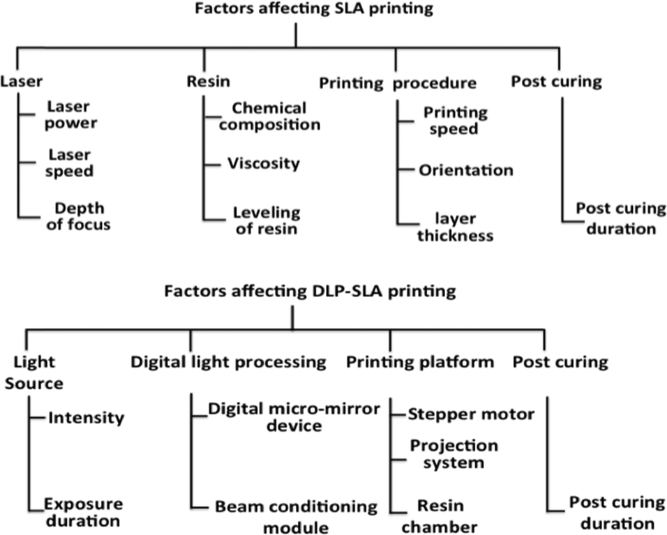
The performance of laser and DLP-SLA printers can be judged by the dimensional accuracy and surface roughness of the printed object. Both these factors are dependent on object orientation, layer thickness, resin properties and building style as mentioned in Fig. 8.47,48
 | ||
| Fig. 8 Parameters affecting laser and DLP-SLA print process. | ||
Comina et al. used a low cost consumer grade 3D printer (Miicraft, Taiwan) to print a reusable template for casting PDMS.50 The templates had multiple thickness structures ranging from 50 μm to several millimetres in a single print. In order to properly cast the PDMS, the printed resin template needed to be manually coated with a protective ink. Chan et al. used the same printer and demonstrated a three step treatment (heating-plasma-salinisation) of the printed template to facilitate the curing of PDMS.51 They developed a single step molding method from a 3D printed template to generate true 3D PDMS base microfluidic system. Moreover, a novel injection-on-demand microfluidic device was developed, by taking advantages of the cracks formed during the single step molding process.
There has also been considerable work focused on printing open microfluidic channels. These are harder to print than templates, but easier to print than enclosed channels because it is easier to remove the uncrosslinked resin. Comina et al. again used the Miicraft printer to print a complex open microfluidic channel which was then sealed with an adhesive tape.52 The device was printed in XY-plane instead of Z, which reduced the surface roughness and printing time. This printing direction also exploited the resolution limit of the printer.
Shallan et al. demonstrated the first use of the Miicraft printer for the direct fabrication of transparent microfluidic devices having enclosed channels with a dimension of 250 μm.53 The printer accuracy was determined by printing positive and negative features of varying shape and dimensions (Fig. 9). The dimension of printed channels was 50 or 100 μm greater/smaller than original design due to positioning of the sliced image over the pixels. The roof of the sealing channel was rough because of back side effect – i.e., the penetration of light into resin to a depth greater than the layer thickness. This could be improved by changing curing depth, intensity, exposure wavelength, time and the resin itself. The transparent propriety resin exhibits 60% transmission from 430–620 nm for a 50 μm thick layer. The Miicraft was presented as a good compromise between price, resolution and printing time for microfluidics, printing a range of microfluidic functional units including droplet generators, gradient generators, and a complex microchip that had variable detection path lengths and could also perform standard addition for the quantitation of nitrate in water.
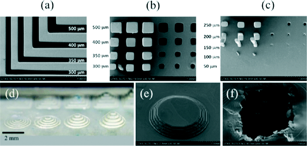 | ||
| Fig. 9 (a–c) SEM images of basic positive and negative 3D printed structures printed with an exposure time of 3.5 s and at a 45° angle with respect to the pixels. (a) L-shaped trenches designed with x or y dimensions of 300, 350, 400, and 500 μm. Resulting structures are 50 or 100 μm narrower than the original design. (b) Rows with three columns and three holes (same x and y dimensions in each row). The x and y dimensions from top to bottom were designed to be 500, 400, 350, and 300 μm with a fixed z dimension of 2000 μm. (c) Rows with three columns and three holes (same x and y dimensions in each row). The x and y dimensions from top to bottom were designed to be 250, 200, and 150 μm, while the 100 and 50 μm columns were not printed, with a fixed z dimension at 2000 μm. A size error of 50 or 100 μm, corresponding to one or two pixels, respectively, was adversely introduced by the slicing software. (d) Photo of five concentric circular steps with varying heights of 50, 100, 150 and 200 μm (from left to right, respectively). (e) SEM image of steps that are 100 μm high each printed with an exposure time of 3.5 s. (f) SEM image of a transverse section of a closed channel designed to be 250 μm wide and deep. The model was printed upside down.53 (Copyright 2014 ACS). | ||
The microfluidic assembly shown in Fig. 10 was directly fabricated by a 3D printer (Asiga, Picoplus 27). It consists of two independent open channels with an additional glass slip that enables the observation of cells under a microscope, assembled on a light addressable potentiometric sensor (LAPS) chip.54 The biocompatibility of the printed microfluidic chip was determined by comparing the cell growth curve obtained from culturing cells within printed microfluidics and in a cell culture flask. The identical growth curve showed that both had similar biocompatibility. The demonstrated process simplicity and biocompatibility make this a promising achievement in rapid prototyping manufacturing for microfluidics.
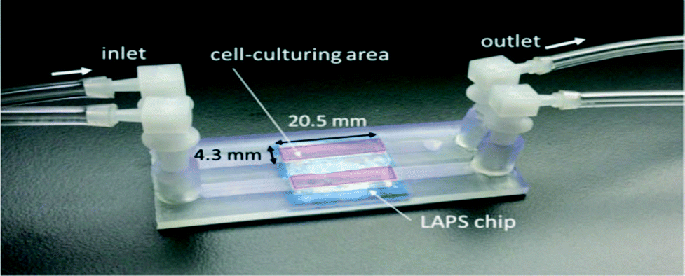 | ||
| Fig. 10 LAPS chip with attached microfluidic channels.54 (Copyright 2015 WILEY). | ||
Miicraft was used to fabricate a solid phase extraction (SPE) pre-concentrator consisting of two extraction channels, micromixer and fittings for connectors.55 Each extraction channel was filled with 29 layers of ordered cuboids (0.4 × 0.4 × 0.2 mm), including 526 cuboids in total. The fabrication time of each preconcentrator was around 38 min. The acrylate base resin (electron donor group) within the printed device was capable of extracting trace elements. The specific polymer-metal ion interactions (electron donor–electron acceptor interactions) provided the selectivity for the extraction of trace metals ions from samples in high salt solution.
Rogers et al. fabricated microfluidic devices with integrated membrane base valves.56 The device was directly printed on a glass substrate. The resin was modified to print the smallest channel (350 × 250 μm) with 100% accuracy. Due to modification of the resin, the printed device was not fully transparent and showed bulk fluorescence, but this was the first demonstration of a 3D printed fluidic device with an integrated pneumatic valve. Au et al. printed fluidic valves and pumps for the automation of microfluidic devices using the Viper SLA printer.57 The valves were added into a digital design as a module to form multi-way switches and pumps. These fluid automation devices were user-friendly. Printing resolution and material choices were still the critical constraints and made the performance of these printed valves inferior to PDMS. Recently Comina et al. has introduced the integration of check valves for a unibody lab on chip (ULOC) fabricated through Miicraft.58 In another work, Comina et al. printed a ULOC consisting of two modules, a microfluidic level and the optics.59 The device manually commands the preparatory sequence of mixing two reagents and three analyte concentrations with minimal user intervention, limited to finger actuation at a single point. The focusing optics created with the same 3D printer, was conceived to image the ULOC detection region on different cell phone cameras. They demonstrated a sensible combination of technologies to enable practical autonomous LOC sensing on cell phones.
Au et al. evaluated the resolution limit of laser-rastering SLA printer (Viper SL system) in optically clear printed devices using a mail-order facility.60 The CAD file was sent to an external manufacturer with printed devices received a few days later. They found that microchannels between 50 to 200 μm sealed during post curing, while channels having a dimension above 400 μm exhibited a deviation from the expected width of less than 30 μm each (Fig. 11). The optical clarity of the devices was improved by coating the outer surface with a silicon oil. The Watershed XC material met biocompatibility standards but it had poor gas permeability, which prohibited long term cell study on a chip.
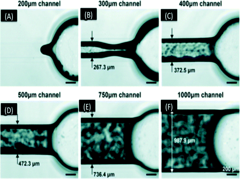 | ||
| Fig. 11 (A–F) Micrographs of 500 μm tall channels built in a range of widths. The actual width of each channels showed deviation of almost 30 μm from design. The 300 μm wide channel could only be partially cleared of resin, while the smaller channels did not clear at all and larger channels were fully cleared.60 (Copyright 2015 RSC). | ||
Patrick et al. printed fluidic open channel devices using consumer-grade laser-rastering SLA 3D printer (Form1+ Formlabs) and compared this to a i3DP on-demand 3D printing service (Frosted Ultra Detail, Shapeways, New York).61 It was observed that the smallest circular channel that the Form+1 printer could print had a diameter 900 μm and the smallest square was 650 μm. The smallest circular channel with the Shapeways printer was 300 μm and the smallest square was 250 μm. The surface roughness was compared through SEM images as shown in Fig. 12. Striation was clearly visible with the Form1+ as seen in Fig. 14A and B which increased the surface roughness. Each fluidic design cost less than $6. This work demonstrates the care that must be taken when selecting the right SLA printer to use.
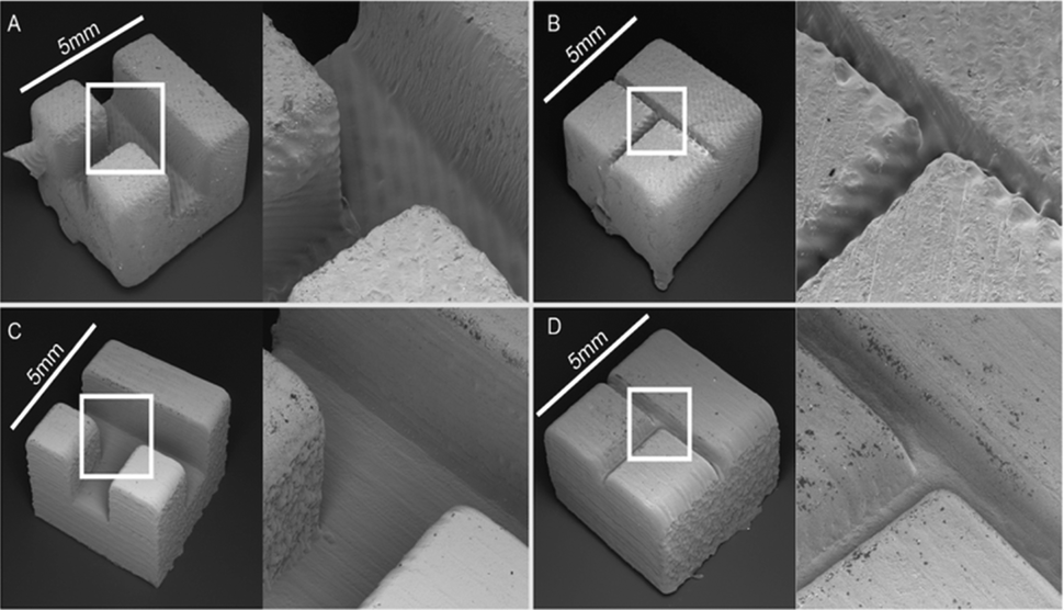 | ||
| Fig. 12 SEM images of open channels printed using the Form1+ (A and B) and Shapeways Frosted Ultra Detail (C and D). Each piece was designed to be 5 mm on a side. Channels were designed to be 1500 microns wide in A & C and 300 microns wide in B & D.61 (Copyright 2015 Patrick et al.) | ||
Materials for SLA are typically proprietary often with poorly characterised surface properties. Wang et al. demonstrated a facile and effective approach to fabricate structural devices by 3D printing.62 An initiator monomer was added into the Miicraft resin to allow simple modification of the surface. This could produce material with any desired surface properties such as from extremely hydrophobic properties to extremely hydrophilic properties. This method made 3D printing technology more practical in the field of microfluidics.
Recently, Macdonald et al. assessed the biocompatibility of various resins, including Watershed 11122XC and Fototec SLA 7150 Clear, against zebrafish embryos.37 The results showed that all of the photopolymers were highly toxic to the embryos, resulting in fatality. While the exact composition of the resin was a trade secret, the material safety data sheet (MSDS) indicated that these resins contain acrylate and methacrylate which are toxic.63 However, the post-printing treatment of Fototec 7150 with ethanol increased the biocompatibility and made it suitable for zebrafish culture.64
Due to some attractive features of PDMS, such as its gas permeability and flexibility, a PDMS resin has been developed.65 Such direct 3D printing of PDMS enabled rapid production of novel chip geometries for a lab on a chip applications. However addition of orange dye in the resin, necessary to print PDMS with an acceptable resolution, sacrificed the optical clear nature of PDMS. This is due to the photoblocker used (Sudan I) and with a different blocker, this could potentially yield optically transparent PDMS.
Recently, Gong et al. determined the effect of optical property of resin on channel size and formulated custom resin containing poly(ethylene glycol) diacrylate (PEGDA), 1% Igracure 819 and varying concentrations of photoblocking agent Sudan I.66 It was demonstrated that there is fundamental trade-off between the homogeneity of the optical dose within individual layers and the critical dose that penetrates into a flow channel during fabrication. The minimum channel size 60 μm × 108 μm for 10 μm build layers was achieved by increasing resin absorbance and increasing x–y plane resolution of the projected image from the DLP micro-mirror array. It was consistently printed with PEGDA by addition of 0.6% Sudan I. This work is significant in the push towards printing microfluidic features less than 100 μm.
A sample library of standardised microfluidic components and connectors was manufactured by using stereolithography by Lee et al.31 and also Bhargava et al.67 These were used to create a number of modular, reconfigurable microfluidic units containing fluidic and sensor elements, adaptable to many different microfluidic circuits. This system can make discrete microfluidics; a valuable development vehicle for complex designs. With a wider library of passive and active components, this system can replace monolithically integrated devices for many microfluidic applications. In addition, this system will benefit significantly from additive manufacturing technologies, allowing for the further miniaturisation of elements and development of a larger selection of elements and materials.
Despite its attraction for microfluidics, there are still a number of issues that need to be resolved. First the resolution is limited by both the physical resolution of the DLP/Laser and also the properties of the resin. It is important to note that hardware resolution isn’t the main limitation at the moment, but achieving this with a usable build space for microfluidics within a reasonable timeframe. Using the 2PP nanoscribe system, it is possible to create objects with sub μm structures and voids, albeit over a few mm, at a very high price. Continued development will see this improve, as well the advent of continuous liquid interface printing (CLIP) which demonstrated print speeds 10× quicker than all current SLA printers.68 This translates to a 30 × 40 × 5 mm microchip being printed in 2–3 min. Continued development of this type of printing with improved resolution will see 3D printers emerge as a low-cost and useful fabrication technique for microfluidics, however this can only be done with a concurrent improvement in resin chemistry. The main challenge with printing enclosed microfluidic structures is to remove the uncured resin. This is easier than i3DP because the resin is a liquid, but it is still challenging for small structures. Lower viscosity resins are required, with the improved ability to constrain light to only the exposed region (and depth) being critical to be able to realise any future improvements in hardware.
As yet unknown, is the influence on the surface roughness of the fabricated part resulting from the movement of the stepper motor. This is again addressed with CLIP printing (Fig. 13), although the impact of the steps and rough surfaces on microfluidic performance has yet to be clearly understood, it nevertheless allows a level of control over surface roughness that is unprecedented.
 | ||
| Fig. 13 (A) Schematic illustration of CLIP printer. (B–C) CLIP enables fast print speeds and layerless part construction.68 (Copyright 2015 AAAS). | ||
Although the stereolithography process was introduced almost 25 years ago, there is still enough room for further enhancement in the process. Recently, novel microdiamond based composite resin was used by Miicraft to print thermally conducting prototype.69 It indicates that proprietary resin can be exploited according to the particular application. One of the major limitations of all current SLA printers is that they are restricted to a single print material at a time. Choi et al. have developed a prototype multimaterial SLA printer which uses four different resin baths, but the process is complex and each layer requires multiple exposures in each resin, making it inefficient.70 Continued development in this area is required for SLA to be the ideal method of choice for microfluidics.
Two-photon polymerisation (2PP)
Fundamentals of 2PP printing
Two-photon polymerisation (2PP) is a laser based technique which uses a near-infrared femtosecond laser. The transparent photocurable epoxy resin enables the direct creation of 3 dimensional structures. 2PP was first described theoretically by Maria Göppert-Mayer in 1931 (ref. 71) and first demonstrated practically in 1961 by Kaiser and Garrett.72 The fully focused femtosecond laser pulses scanned the photosensitive resin from the bottom slice to the upside slice. The two photons are absorbed simultaneously by the molecule which induces photochemical reaction between photo-initiator and monomers.73 The synergic effect of optical, chemical and material non-linearities makes it possible to achieve reproducible resolution of tens of nanometers.74 The fundamental difference between SLA and 2PP is that in SLA a single photon is used to build 3D structure. Furthermore, in 2PP solid resist can replace epoxy resin for the direct fabrication of micro and nano-structures.The schematic illustration of 2PP is given in Fig. 14, which consists of a laser source, beam direction system (left column), in situ monitoring system (middle column), beam steering and motion stage (right column).
 | ||
| Fig. 14 Schematic femtosecond laser direct writing system. The femtosecond laser focused by a lens (1.4, oil immersion used here). The laser scanning path was precisely controlled by computer according to the pre-programmed structures from the bottom slice to the upside slice until the entire 3D structure is achieved. The imaging system using a charge couple device (CCD) is useful both for optical adjustment and for in situ fabrication monitoring. PBS: polarization beam splitter; OL: objective lens; PZT: piezoelectric transducer.75 (Copyright 2015 Elsevier). | ||
Most of the materials used for 2PP are designed for conventional lithographic applications and both negative and positive photoresists. In the case of negative photoresists, the two-photon exposure results in the crosslinking of polymer chains through radical polymerisation, making the exposed area insoluble in the solvent and writing the structure directly in the sample. With positive photoresists, the opposite occurs; two-photon absorption causes the photoresist polymeric chains to break and become soluble in the development solvent, so the reverse structure is written in the sample. Negative photoresists containing acrylic oligomers or epoxy resins are the most popular photoresists for 2PP. Their fundamental ingredients contain photo-initiators used for radical generation, and monomers and cross-linkers constituting the main skeleton of micro or nanostructures. Commercially available resins have the disadvantage that they cannot be easily modified or combined with active components for added functionality. However new, organic/inorganic hybrid sol–gel materials are specifically designed for 2PP applications. These materials have high optical quality, post-processing chemical and electrochemical inertness, and good mechanical and chemical stability.76,77
In 2PP fabrication, microstructures are built from voxel (unit volume of a material) that can overlap each other. The fabrication accuracy of 2PP is determined by the voxel size. The high spatial resolution, precision and accuracy of 2PP can improved by considering the factors mentioned in Fig. 15.
 | ||
| Fig. 15 Parameters affecting 2PP print process. | ||
Until now considerable work has been done on improving the resolution of 2PP by optimising different parameters. Kawata et al.78 achieved a milestone with a resolution of 120 nm. Other attempts include the use of new photoinitiators,79,80 continuous scanning mode,81 shorter wavelength,82 longer exposure time,83 and confining the polymerization phenomenon using a quencher molecule in the photopolymerisable system.27,84 Sugioka et al. comprehensively reviewed fundamentals and the fabrication of 3D micro and nanocomponents based on 2PP.85
 | ||
| Fig. 16 (a–b) Schematic illustration of a 3D microchannel structure fabricated by two-photon using positive photoresists. Microfluidic structure consists of two rectangular cavities (width, 100 μm; length, 20 μm; depth, 20 μm) and a sloped side wall that are connected by 12 microchannels. (b) Scanning electron micrograph of the final structure, viewed normal to the substrate and two-photon fluorescence images of the final structure at and below the surface.89 (Copyright 2002 AAAS) (c–d) A conceptual microfluidic device fabricated by 2PP of SU-8. SEM view of the 3D microfluidic systems with 100 μm diameter disk and 15 μm height. Here, the internal portion of the background volume is solidified by additional ultraviolet exposure.90 (Copyright 2009 RSC). | ||
Despite the fact that commercial negative photoresists have better modeling and conformal capacities, they are not frequently used for fabrication of microfluidic structure as prolonged processing time is required due to additive type fabrication. However, Wu et al. proposed a profile scanning method for the prototyping of a microfluidic chip (Fig. 16c and d) using negative-tone photoresists.90 The surface profile scanning followed by additional UV irradiation reduces the processing time for formation of structures with large interior volumes, but this process is not effective for high porosity or thin structures. Ober et al. presented a very interesting approach utilising PDMS base resin instead of classical photoresist for microfluidic channels having dimensions of few tens of microns.91
2PP technologies used by different researchers for direct fabrication of microfluidic chips or masters are mentioned in Table 1.
2PP has been used for the formation of micro or nano-devices which can be integrated into open or closed microfluidic channels prepared by other techniques. The typical example of the integration of various functional units includes micro-sieves,92 micro-over-passes,93 micro-mixers,94–96 micro-heaters,97 optofluidic devices,98 surface enhanced Raman scattering (SERS) monitors99 and catalytic micro-reactors.100 The hybrid approach that involves the combination of other techniques for making a single microfluidic is not the focus of this article. Xu et al.101 and Sugioka et al.102 critically review the integration of functional micro-devices within a microfluidic chip.
Despite these unique capabilities of 2PP and its potential applications in microfluidics, it is not viewed as the best fabrication tool at this stage, unless it is for its outstanding resolution. This is due to a number of factors: first, it is extensively time consuming process, with for instance, the time required to fabricate a 1 mm3 volume microfluidic structure exceeding 104 days.85 Several methods like surface profile scanning, multifocal scanning and use of parallel multi beams have been developed for increasing the speed but are not widely available. Second, the high costs of femtosecond lasers, positioning systems and optics is another hindering factors. Furthermore, it needs absolute clean room conditions. Finally, as with SLA, multi-material print capability is difficult. These barriers have prevented the use of 2PP in the field of microfluidics outside of niche applications that require the construction of nm–μm sized structures.
Extrusion printing
Fundamentals of extrusion printing
In 1989, Scott Crump filed a patent for a technology called fused deposition modeling (FDM).103 He co-founded the company Stratasys Ltd to commercialise the technology. Currently it is one of the most widely used additive manufacturing technologies. In FDM a thermoplastic material is extruded through a high temperature nozzle to build a 3D model layer-by-layer.104 The nozzle contains a temperature control unit that maintains the temperature of thermoplastic material just above its melting point so that it can flow easily through the nozzle. The molten material, after flowing from the nozzle, immediately solidifies in the desired area. Once a layer is built, the platform lowers, and the extrusion nozzle deposits another layer. This process continues until the whole object is formed (Fig. 17). The layer thickness and vertical dimensional accuracy is determined by the extruder die diameter. While FDM is the most popular extrusion type printer, it is also important to recognise that since its original inception, there have also been other extrusion printers developed that can print gels and other biocompatible structures, although these will not be discussed in detail here.105,106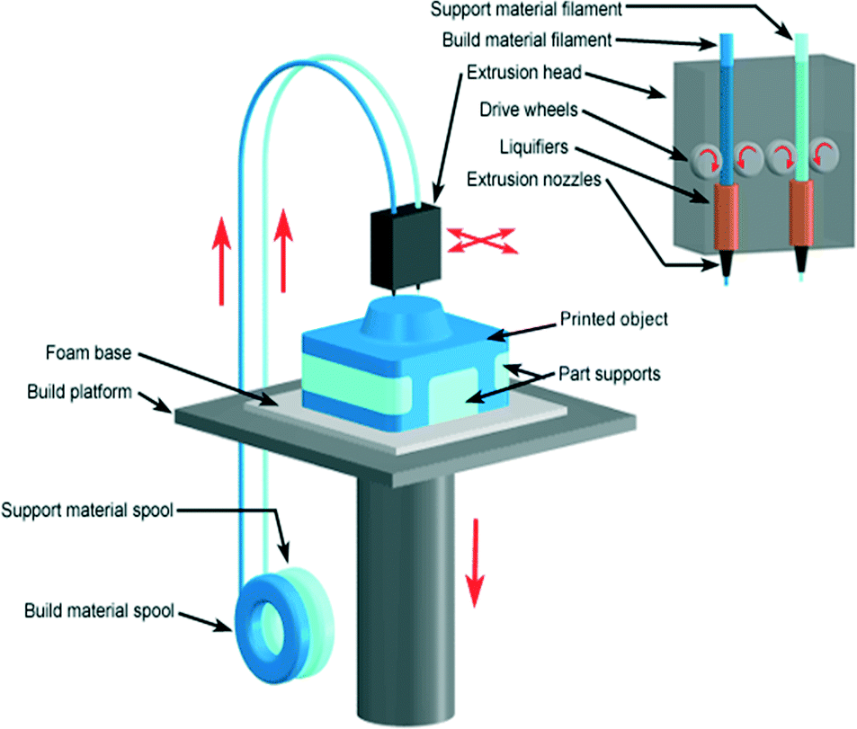 | ||
| Fig. 17 Schematic illustration of FDM 3D printer. The feedstock filament of thermoplastic material is drawn from a spool into the FDM extrusion head, in which it is heated into a semiliquid state and then by drive wheels it is extruded out through nozzle on a built platform.20 (Copyright 2008 Custom Part Net). | ||
A notable advantage of FDM is that it can process almost all types of thermoplastic polymers. This is important because thermoplastics are used for mass replication fabrication with hot embossing or injection molding. This means that FDM chips can be made in materials that are compatible with mass production techniques. Acrylonitrile butadiene styrene (ABS), polystyrene (PS) and polycarbonate (PC) are commonly used materials107 and there is a wide range of biocompatible polymers including polycarpolactone (PCL), polylactic acid (PLA), polybutylene terephthalate (PBT) and polyglycolic acid (PGA).108 Beside these conventional materials, access to composite materials such as reinforced polymer composites109 and nano composites make FDM an attractive choice for the fabrication of objects for different applications.
FDM machines offer a number of process parameters (Fig. 18), which allow the user to fabricate devices ranging from solid to honeycomb structures with varying strength, surface quality, accuracy, and mechanical properties. These are also capable of printing multi-materials, traditionally equipped with multiple heads to accommodate the different polymer based materials, but more recently several early stage nozzle designs have been published enabling material switching inside the nozzle. While it is common that one of the materials is a support material (and most software assumes that this is the case), it is possible to print multi-material devices without a support opening the way to integrated functional fluidic devices.
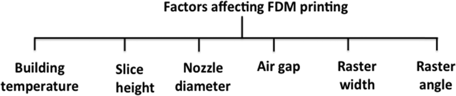 | ||
| Fig. 18 Parameters affecting FDM process. | ||
The simplicity, low cost and availability of a wide range of materials, encourages researchers to use FDM technology in the field of microfluidics. Lee et al., performed an extensive study by printing microfluidic features via FDM printer (Dimension Elite, Stratasys) for evaluating printing resolution, accuracy, surface roughness and biocompatibility of ABS plus-P430 filament.28 It was observed that the accuracy of printed features had an average deviation of 60.8 μm and 71.5 μm along the Y and X axis, respectively. The printed channels had a rough surface with protruding filament strands (Fig. 19).
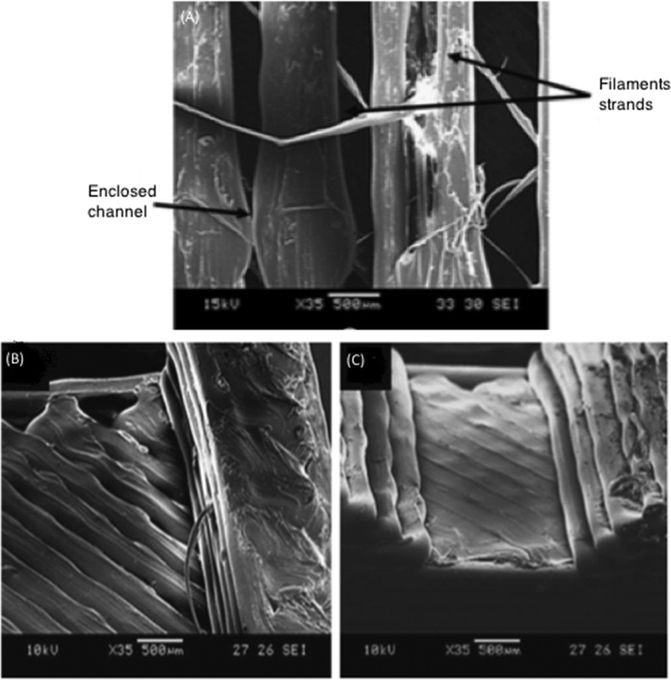 | ||
| Fig. 19 (A) Channels printed by FDM, (B–C) Staircase effect causing roughness in channels.28 (Copyright 2015 Springer). | ||
Symes et al. demonstrated the production of reusable, robust and self-healing bespoke reactionware through Fab@Home extrusion printer using acetoxysilicone polymer.111 The reactionware, with built-in catalyst, enabled the reaction to be monitored in situ and was used for organic and inorganic synthesis. In another study, Kitson et al. fabricated polypropylene based reactionware, having cylindrical channels 0.8 mm in diameter and a total reaction volume of 60 μL.112 A benefit to these organic reactionware devices was that they can be fabricated in a few hours and, due to the millimeter scale of the devices, can avoid blockages due to the formation of precipitates. Furthermore, the potential of 3D manufacturing was demonstrated by stopping mid-print to deposit solid reagents into a chamber which was then sealed with the printer, something not easily done with i3DP or STL. Fabrication of such miniaturised reactionware provides an alternate to the traditional passive-vessel approaches.113
FDM was used for the fabrication of capillary valves in centrifugal microfluidic disc.114 Microfluidic structures containing valve channels with different widths, heights and radial distances from the center of rotation were compared with the capillary valve theories.115 Trapezoidal modules each containing one microfluidic architecture having widths of 254 μm and 508 μm with variable heights of 254, 408, 762 and 1016 μm were printed. Due to the printing process, the produced valve channels possessed a ridged pattern. It was concluded that as the height of the valve channel was reduced, the critical rpm was found to become progressively more width-dependent. Operable centrifugal valves with ridged surfaces could be printed for complex fluid handling.
He et al. demonstrated a simple, low cost microfluidic chip with a novel 3D sugar printer.116 A desktop extrusion printer was modified with a redesigned extruder that extruded melted sugar (maltitol) with pneumatic force. Sugar lines were printed on PDMS base layer followed by casting PDMS onto the sugar layer. This process was repeated and microchannels were sealed. The sacrificial sugar was removed by placing the chip in boiling water; printed structure size was 25 × 25 × 2.2 mm having microchannels with a diameter of 200 μm. The printing quality was dependent on printing speed, and impressively small channels a few microns wide could be achieved using a very small sized nozzle. With a nozzle size of 0.3 mm, a minimum microchannel diameter was 40 μm. The 3D printed microfluidic chip was used for cell culturing.
A low cost and sensitive microfluidic immunosensor for multiple protein detection was printed through MakerBot Replicator 2X.117 The device was composed of PLA, with 40 mm length × 30 mm width at the base, having three reagent chambers connected to a microfluidic channel with a height of 200 μm and a volume of 160 μL. The device had could detect three prostrate cancer biomarkers simultaneously in 35 min.
Kise et al. fabricated a sandwich-format mixer having three different designs with 3D printed spacer using FDM technology, coupled with three different spectroscopic probes.118 A polymer spacer was sandwiched between two transparent windows, which created a closed microfluidic system. The channels of the mixer were defined by regions in the polymer spacer that lacked material. Each mixer design had a diameter of 25 mm and layer thickness was 200–250 μm. Two optically transparent windows sandwiched a spacer for the assembly of the mixer. The sandwich format alleviated the requirement of optical transparency of mixer material. This device offered versatility in microfluidic mixing.
Bishop et al. reported semi transparent fluidic device using poly(ethyleneterephthalate) with threaded ports which enable the integration of commercially available tubing as well as specially designed 3D printed fittings.119 These devices included channels having dimensions of 800 × 800 μm square cross sections and were semi-transparent to allow visualization of the solution-filled channel. A low cost replicator 2X desktop 3D printer (MakerBot) was used for fabrication of the device. Prussian blue nanoparticles were prepared in a 3D printed mixing channel and applied to electrode surfaces for H2O2 sensing via flow-injection amperometry.
Chips printed by FDM were used to rapidly monitor the presence of pathogen microorganisms. Chudobova et al. utilised ABS polymer and printed a chip via a Profi3Dmaker printer. The 3D-printed chip was suitable for bacterial cultivation, DNA isolation, PCR, and detection of amplified gene using gold nanoparticle (AuNP) probes from 10–500 μL of sample. A specific interaction between mecA gene with the AuNP probes was used for detection of pathogen.120 Krejcova et al. printed a chip with dimensions 42.64 × 14.95 × 4.87 mm for the detection of influenza virus.121 The principle of microfluidic chip was based on a two-step procedure that includes isolation based on magnetic beads and electrochemical detection. Such fabrication provided a promising and powerful platform for the diagnostic purposes.
Dolomite has recently launched the fluidic factory that offers the first microfluidic targeted FDM 3D printer. An innovative printer head design allows reliable printing of cyclic olefin copolymer (COC) while new software has changed the focus to producing finished surfaces on the inside, while all other 3D printing approaches at this stage focus on the external surface being the best.122 The potential and success of the printer will be determined over the next few years, but it has the potential to replace PDMS as the method of choice for in-house fabrication of polymer devices.
While showing great promise for microfluidics, dimensional accuracy and surface finish is often compromised during FDM printing, and the minimum channel dimensions are still quite large by microfluidic standards. As the stage must move linearly throughout the XY plane, before moving to the next Z layer, print time is dependent on the build size, and is quite slow in comparison to i3DP and SLA. Despite these limitations, it is currently the only 3D printing approach in which materials can be placed inside the half-printed structure prior to finishing the print run.
Conclusions
The last 2–3 years have shown a phenomenal growth and interest in 3D printing in general and this has echoed within the microfluidic community. The unprecedented ease in fabrication of complex microfluidic devices, and the low price tag of consumer-focused desktop printers combined with a rapidly increasing number of 3D printing service providers makes 3D printing affordable for many researchers around the world. Despite the enthusiasm of the early uptakers, its applicability is limited in part by the technical inability to reliably print microfluidic channels with dimensions less than several hundred microns in a reasonable sized device. No printer type is perfect with i3DP, SLA, 2PP and FDM having unique capabilities and features when it comes to printing microfluidic devices. i3DP allows for printing channels as small as 25 μm in a range of materials, but is hindered by the difficulties in the removal of the support material from small fluidic features as well as by a relatively wasteful print process. SLA enables similar feature sizes without the need for a support material, but the materials are limited to UV curable resins. 2PP currently can achieve the smallest enclosed channels and features in the nano range however, the limited build volume and infrastructure required for operation restrict the practicality of using it for microfluidic devices. Lastly, FDM printing allows for the use of a wide range of thermopolymers and provides therefore a material compatibility with mass manufacturing. Unfortunately, the resolution that can be obtained with FDM is 100 μm with rough channel surfaces, reducing its appeal for microfluidics. To secure a future in microfluidics, printer specifications will need to improve to enable the fabrication of enclosed microchannels down to 10 μm, in a range of materials with varying physical and chemical properties, and allow for the printing of integrated multifunctional and multi-material devices. Whether this can be done at a cost and speed that will make it a viable manufacturing approach has yet to be seen, but 3D printing certainly has the potential to replace soft lithography in PDMS as rapid prototyping technique because of the material compatibility with commercial production.Acknowledgements
This study is supported by ARC Centre of Excellence for electromaterials Science (ACES) (Grant CE140100012). MCB would like to thank the ARC for a Future Fellowship (FT130100101).References
- H. Becker, Lab Chip, 2009, 9, 2119–2122 RSC.
- C. W. Hull, US Pat., 06/638905, 1986 Search PubMed.
- J. Harrop and R. Gordon, 3D Printing 2015-2025: Technolgies, Markets, Players. Current usage future application and market forecasts IDTechEX, 2014 Search PubMed.
- 3D printing market to grow to 16.2 billion USD in 2018, Met. Powder Rep., 2014, vol. 69, p. 42, Available at: http://www.sciencedirect.com/science/article/pii/S0026065714701389 Search PubMed.
- P. Kim, K. W. Kwon, M. C. Park, S. H. Lee, S. M. Kim and K. Y. Suh, BioChip J., 2008, 2, 1–11 Search PubMed.
- H. Becker and L. E. Locascio, Talanta, 2002, 56, 267–287 CrossRef CAS PubMed.
- M. Focke, D. Kosse, C. Muller, H. Reinecke, R. Zengerle and F. von Stetten, Lab Chip, 2010, 10, 1365–1386 RSC.
- A. Waldbaur, H. Rapp, K. Länge and B. E. Rapp, Anal. Methods, 2011, 3, 2681–2716 RSC.
- M. Vaezi, H. Seitz and S. Yang, Int. J. Adv. Des. Manuf. Technol., 2013, 67, 1721–1754 CrossRef.
- V. Gupta, M. Talebi, J. Deverell, S. Sandron, P. N. Nesterenko, B. Heery, F. Thompson, S. Beirne, G. G. Wallace and B. Paull, Anal. Chim. Acta, 2016, 910, 84–94 CrossRef CAS PubMed.
- A. K. Au, W. Huynh, L. F. Horowitz and A. Folch, Angew. Chem., Int. Ed., 2016, 55, 3862–3881 CrossRef CAS PubMed.
- M. Singh, H. M. Haverinen, P. Dhagat and G. E. Jabbour, Adv. Mater., 2010, 22, 673 CrossRef CAS PubMed.
- http://www.custompartnet.com/wu/jetted-photopolymer, (accessed November, 2015).
- B.-J. De Gans, P. C. Duineveld and U. S. Schubert, Adv. Mater., 2004, 16, 203–213 CrossRef CAS.
- K. K. B. Hon, L. Li and I. M. Hutchings, CIRP Ann., 2008, 57, 601–620 CrossRef.
- C.-T. Chen, ch. Inkjet printing of microcomponents: theory, design, characteristics and applications, in Features of Liquid Crystal Display Materials and Processes, ed. N. Kamanina, InTech, 2011, pp. 43–60 Search PubMed.
- A. Pfister, R. Landers, A. Laib, U. Hübner, R. Schmelzeisen and R. Mülhaupt, J. Polym. Sci., Part A: Polym. Chem., 2004, 42, 624–638 CrossRef CAS.
- E. Sachs, M. Cima, P. Williams, D. Brancazio and J. Cornie, J. Eng. Ind., 1992, 114, 481–488 CrossRef.
- T. Femmer, I. Flack and M. Wessling, Chem. Ing. Tech., 2016, 535–552 CrossRef CAS.
- http://www.custompartnet.com/wu/3d-printing, (accessed November, 2015).
- http://www.stratasys.com/materials/polyjet/digital-materials, (accessed November 2015).
- J. C. McDonald, M. L. Chabinyc, S. J. Metallo, J. R. Anderson, A. D. Stroock and G. M. Whitesides, Anal. Chem., 2002, 74, 1537–1545 CrossRef CAS PubMed.
- A. Bonyár, H. Sántha, B. Ring, M. Varga, J. G. Kovács and G. Harsányi, Protein Eng., 2010, 5, 291–294 Search PubMed.
- A. Bonyár, H. Sántha, M. Varga, B. Ring, A. Vitéz and G. Harsányi, Int. J. Mater. Form., 2014, 7, 189–196 CrossRef.
- R. Walczak and K. Adamski, J. Micromech. Microeng., 2015, 25, 085013 CrossRef.
- G. D. Hoople, D. A. Rolfe, K. C. McKinstry, J. R. Noble, D. A. Dornfeld and A. P. Pisano, Comparison of Microscale Rapid Prototyping Techniques for Microfluidic Applications, American Society of Mechanical Engineers, 2014 Search PubMed.
- K. Takada, H.-B. Sun and S. Kawata, Appl. Phys. Lett., 2005, 86, 071122 CrossRef.
- J. M. Lee, M. Zhang and W. Y. Yeong, Microfluid. Nanofluid., 2016, 20, 1–15 CrossRef CAS.
- Y. Hwang, O. H. Paydar and R. N. Candler, Sens. Actuators, A, 2015, 226, 137–142 CrossRef CAS.
- J. O'Connor, J. Punch, N. Jeffers and J. Stafford, J. Phys.: Conf. Ser., 2014, 525, 012009 CrossRef.
- K. G. Lee, K. J. Park, S. Seok, S. Shin, J. Y. Park, Y. S. Heo, S. J. Lee and T. J. Lee, RSC Adv., 2014, 4, 32876–32880 RSC.
- S. A. Gowers, V. F. Curto, C. A. Seneci, C. Wang, S. Anastasova, P. Vadgama, G.-Z. Yang and M. G. Boutelle, Anal. Chem., 2015, 87, 7763–7770 CrossRef CAS PubMed.
- O. Paydar, C. Paredes, Y. Hwang, J. Paz, N. Shah and R. Candler, Sens. Actuators, A, 2014, 205, 199–203 CrossRef CAS.
- R. D. Sochol, E. Sweet, C. C. Glick, S. Venkatesh, A. Avetisyan, K. F. Ekman, A. Raulinaitis, A. Tsai, A. Wienkers, K. Korner, K. Hanson, A. Long, B. J. Hightower, G. Slatton, D. C. Burnett, T. L. Massey, K. Iwai, L. P. Lee, K. S. J. Pisterbi and L. Lin§, Lab Chip, 2016, 16, 668–678 RSC.
- B. C. Gross, K. B. Anderson, J. E. Meisel, M. I. McNitt and D. M. Spence, Anal. Chem., 2015, 87, 6335–6341 CrossRef CAS PubMed.
- J. L. Erkal, A. Selimovic, B. C. Gross, S. Y. Lockwood, E. L. Walton, S. McNamara, R. S. Martin and D. M. Spence, Lab Chip, 2014, 14, 2023–2032 RSC.
- N. P. Macdonald, F. Zhu, C. J. Hall, J. Reboud, P. S. Crosier, E. E. Patton, D. Wlodkowic and J. M. Cooper, Lab Chip, 2016, 291–297 RSC.
- P. J. Bártolo, Stereolithography: Materials, Processes and Applications, Springer, 2011 Search PubMed.
- F. P. Melchels, J. Feijen and D. W. Grijpma, Biomaterials, 2010, 31, 6121–6130 CrossRef CAS PubMed.
- Y. M. Huang, S. Kuriyama and C. P. Jiang, Int. J. Adv. Des. Manuf. Technol., 2004, 24, 361–369 CrossRef.
- X. Zheng, J. Deotte, M. P. Alonso, G. R. Farquar, T. H. Weisgraber, S. Gemberling, H. Lee, N. Fang and C. M. Spadaccini, Rev. Sci. Instrum., 2012, 83, 125001 CrossRef PubMed.
- Y. Pan, C. Zhou and Y. Chen, J. Manuf. Sci. Prod., 2012, 134, 051011 CrossRef.
- T. Billiet, M. Vandenhaute, J. Schelfhout, S. Van Vlierberghe and P. Dubruel, Biomaterials, 2012, 33, 6020–6041 CrossRef CAS PubMed.
- C. Sun, N. Fang, D. Wu and X. Zhang, Sens. Actuators, A, 2005, 121, 113–120 CrossRef CAS.
- A. Waldbaur, B. Carneiro, P. Hettich and B. E. Rapp, Computer aided microfluidics (CAMF)–High-resolution projection lithography for the rapid creation of large-scale microfluidic structures, Japan, 2012 Search PubMed.
- A. Waldbaur, B. Waterkotte, K. Schmitz and B. E. Rapp, Small, 2012, 8, 1570–1578 CrossRef CAS PubMed.
- L. Lu, J. Fuh, A. Nee, E. Kang, T. Miyazawa and C. Cheah, Mater. Res. Bull., 1995, 30, 1561–1569 CrossRef CAS.
- T. H. Pang, 3D Systems Inc, 1994 Search PubMed.
- http://www.peachyprinter.com, (accessed February, 2016).
- G. Comina, A. Suska and D. Filippini, Lab Chip, 2014, 14, 424–430 RSC.
- H. N. Chan, Y. Chen, Y. Shu, Y. Chen, Q. Tian and H. Wu, Microfluid. Nanofluid., 2015, 19, 9–18 CrossRef CAS.
- G. Comina, A. Suska and D. Filippini, Lab Chip, 2014, 14, 2978–2982 RSC.
- A. I. Shallan, P. Smejkal, M. Corban, R. M. Guijt and M. C. Breadmore, Anal. Chem., 2014, 86, 3124–3130 CrossRef CAS PubMed.
- S. Takenaga, B. Schneider, E. Erbay, M. Biselli, T. Schnitzler, M. Schöning and T. Wagner, Phys. Status Solidi A, 2015, 212, 1347–1352 CrossRef CAS.
- C.-K. Su, P.-J. Peng and Y.-C. Sun, Anal. Chem., 2015, 87, 6945–6950 CrossRef CAS PubMed.
- C. I. Rogers, K. Qaderi, A. T. Woolley and G. P. Nordin, Biomicrofluidics, 2015, 9, 016501 CrossRef PubMed.
- A. K. Au, N. Bhattacharjee, L. F. Horowitz, T. C. Chang and A. Folch, Lab Chip, 2015, 15, 1934–1941 RSC.
- G. Comina, A. Suska and D. Filippini, Micromachines, 2015, 6, 437–451 CrossRef.
- G. Comina, A. Suska and D. Filippini, Angew. Chem., Int. Ed., 2015, 54, 8708–8712 CrossRef CAS PubMed.
- A. K. Au, W. Lee and A. Folch, Lab Chip, 2014, 14, 1294–1301 RSC.
- W. G. Patrick, A. A. Nielsen, S. J. Keating, T. J. Levy, C.-W. Wang, J. J. Rivera, O. Mondragón-Palomino, P. A. Carr, C. A. Voigt and N. Oxman, PLoS One, 2015, 10, 1–18 Search PubMed.
- X. Wang, X. Cai, Q. Guo, T. Zhang, B. Kobe and J. Yang, Chem. Commun., 2013, 49, 10064–10066 RSC.
- S. M. Oskui, G. Diamante, C. Liao, W. Shi, J. Gan, D. Schlenk and W. H. Grover, Environ. Sci. Technol. Lett., 2015, 3, 1–6 CrossRef.
- F. Zhu, N. P. Macdonald, J. M. Cooper and D. Wlodkowic, Additive manufacturing of lab-on-a-chip devices: promises and challenges, Society of Photo-Optical Instrumentation Engineers (SPIE), 2013 Search PubMed.
- T. Femmer, A. J. Kuehne and M. Wessling, Lab Chip, 2014, 14, 2610–2613 RSC.
- H. Gong, M. Beauchamp, S. Perry, A. T. Woolley and G. Nordin, RSC Adv., 2015, 5, 106621–106632 RSC.
- K. C. Bhargava, B. Thompson and N. Malmstadt, Discrete elements for 3D microfluidics, PNAS, California, 2014 Search PubMed.
- J. R. Tumbleston, D. Shirvanyants, N. Ermoshkin, R. Janusziewicz, A. R. Johnson, D. Kelly, K. Chen, R. Pinschmidt, J. P. Rolland and A. Ermoshkin, Science, 2015, 347, 1349–1352 CrossRef CAS PubMed.
- U. Kalsoom, A. Peristyy, P. N. Nesterenko and B. Paull, RSC Adv., 2016, 6, 38140–38147 RSC.
- J.-W. Choi, H.-C. Kim and R. Wicker, J. Mater. Process. Technol., 2011, 211, 318–328 CrossRef CAS.
- M. Göppert-Mayer, Ann. Phys., 1931, 401, 273–294 CrossRef.
- W. Kaiser and C. Garrett, Phys. Rev. Lett., 1961, 7, 229 CrossRef CAS.
- S. Maruo and S. Kawata, Two-photon-absorbed photopolymerization for three-dimensional microfabrication, IEEE, 1997 Search PubMed.
- J.-F. Xing, M.-L. Zheng and X.-M. Duan, Chem. Soc. Rev., 2015, 44, 5031–5039 RSC.
- Y.-L. Zhang, Q.-D. Chen, H. Xia and H.-B. Sun, Nano Today, 2010, 5, 435–448 CrossRef CAS.
- M. Farsari and B. N. Chichkov, Nat. Photonics, 2009, 3, 450–452 CrossRef CAS.
- R. J. Narayan, A. Doraiswamy, D. B. Chrisey and B. N. Chichkov, Mater. Today, 2010, 13, 42–48 CrossRef CAS.
- S. Kawata, H.-B. Sun, T. Tanaka and K. Takada, Nature, 2001, 412, 697–698 CrossRef CAS PubMed.
- J.-F. Xing, X.-Z. Dong, W.-Q. Chen, X.-M. Duan, N. Takeyasu, T. Tanaka and S. Kawata, Appl. Phys. Lett., 2007, 90, 131106–131106 CrossRef.
- B. H. Cumpston, S. P. Ananthavel, S. Barlow, D. L. Dyer, J. E. Ehrlich, L. L. Erskine, A. A. Heikal, S. M. Kuebler, I.-Y. S. Lee and D. McCord-Maughon, Nature, 1999, 398, 51–54 CrossRef CAS.
- X.-Z. Dong, Z.-S. Zhao and X.-M. Duan, Appl. Phys. Lett., 2008, 92, 091113 CrossRef.
- W. Haske, V. W. Chen, J. M. Hales, W. Dong, S. Barlow, S. R. Marder and J. W. Perry, Opt. Express, 2007, 15, 3426–3436 CrossRef CAS PubMed.
- S. H. Park, T. W. Lim, D.-Y. Yang, N. C. Cho and K.-S. Lee, Appl. Phys. Lett., 2006, 89, 173133 CrossRef.
- I. Sakellari, E. Kabouraki, D. Gray, V. Purlys, C. Fotakis, A. Pikulin, N. Bityurin, M. Vamvakaki and M. Farsari, ACS Nano, 2012, 6, 2302–2311 CrossRef CAS PubMed.
- K. Sugioka and Y. Cheng, Appl. Phys. Rev., 2014, 1, 041303 Search PubMed.
- G. Kumi, C. O. Yanez, K. D. Belfield and J. T. Fourkas, Lab Chip, 2010, 10, 1057–1060 RSC.
- M. Stoneman, M. Fox, C. Zeng and V. Raicu, Lab Chip, 2009, 9, 819–827 RSC.
- K. Venkatakrishnan, S. Jariwala and B. Tan, Opt. Express, 2009, 17, 2756–2762 CrossRef CAS PubMed.
- W. Zhou, S. M. Kuebler, K. L. Braun, T. Yu, J. K. Cammack, C. K. Ober, J. W. Perry and S. R. Marder, Science, 2002, 296, 1106–1109 CrossRef CAS PubMed.
- D. Wu, Q.-D. Chen, L.-G. Niu, J.-N. Wang, J. Wang, R. Wang, H. Xia and H.-B. Sun, Lab Chip, 2009, 9, 2391–2394 RSC.
- C. A. Coenjarts and C. K. Ober, Chem. Mater., 2004, 16, 5556–5558 CrossRef CAS.
- J. Wang, Y. He, H. Xia, L.-G. Niu, R. Zhang, Q.-D. Chen, Y.-L. Zhang, Y.-F. Li, S.-J. Zeng and J.-H. Qin, Lab Chip, 2010, 10, 1993–1996 RSC.
- Y. He, B.-L. Huang, D.-X. Lu, J. Zhao, B.-B. Xu, R. Zhang, X.-F. Lin, Q.-D. Chen, J. Wang and Y.-L. Zhang, Lab Chip, 2012, 12, 3866–3869 RSC.
- H. Xia, J. Wang, Y. Tian, Q. D. Chen, X. B. Du, Y. L. Zhang, Y. He and H. B. Sun, Adv. Mater., 2010, 22, 3204–3207 CrossRef CAS PubMed.
- Y. Tian, Y.-L. Zhang, J.-F. Ku, Y. He, B.-B. Xu, Q.-D. Chen, H. Xia and H.-B. Sun, Lab Chip, 2010, 10, 2902–2905 RSC.
- T. W. Lim, Y. Son, Y. J. Jeong, D.-Y. Yang, H.-J. Kong, K.-S. Lee and D.-P. Kim, Lab Chip, 2011, 11, 100–103 RSC.
- B. B. Xu, H. Xia, L. G. Niu, Y. L. Zhang, K. Sun, Q. D. Chen, Y. Xu, Z. Q. Lv, Z. H. Li and H. Misawa, Small, 2010, 6, 1762–1766 CrossRef CAS PubMed.
- Y. Hanada, K. Sugioka, I. Shihira-Ishikawa, H. Kawano, A. Miyawaki and K. Midorikawa, Lab Chip, 2011, 11, 2109–2115 RSC.
- B.-B. Xu, Z.-C. Ma, L. Wang, R. Zhang, L.-G. Niu, Z. Yang, Y.-L. Zhang, W.-H. Zheng, B. Zhao and Y. Xu, Lab Chip, 2011, 11, 3347–3351 RSC.
- B.-B. Xu, R. Zhang, X.-Q. Liu, H. Wang, Y.-L. Zhang, H.-B. Jiang, L. Wang, Z.-C. Ma, J.-F. Ku and F.-S. Xiao, Chem. Commun., 2012, 48, 1680–1682 RSC.
- B.-B. Xu, Y.-L. Zhang, H. Xia, W.-F. Dong, H. Ding and H.-B. Sun, Lab Chip, 2013, 13, 1677–1690 RSC.
- K. Sugioka, J. Xu, D. Wu, Y. Hanada, Z. Wang, Y. Cheng and K. Midorikawa, Lab Chip, 2014, 14, 3447–3458 RSC.
- S. S. Crump, US Pat., 07/429012, 1992 Search PubMed.
- D. T. Pham and R. S. Gault, Int. J. Mach. Tool Manu., 1998, 38, 1257–1287 CrossRef.
- B. R. Ringeisen, R. K. Pirlo, P. K. Wu, T. Boland, Y. Huang, W. Sun, Q. Hamid and D. B. Chrisey, MRS Bull., 2013, 38, 834–843 CrossRef.
- A. L. Rutz, K. E. Hyland, A. E. Jakus, W. R. Burghardt and R. N. Shah, Adv. Mater., 2015, 27, 1607–1614 CrossRef CAS PubMed.
- L. Novakova-Marcincinova and I. Kuric, Manuf. and Ind. Eng., 2012, 11, 24–27 Search PubMed.
- H. N. Chia and B. M. Wu, J. Biol. Eng., 2015, 9, 4 CrossRef PubMed.
- W. Zhong, F. Li, Z. Zhang, L. Song and Z. Li, Mater. Sci. Eng., A, 2001, 301, 125–130 CrossRef.
- C. Ziemian and P. Crawn III, Rapid Prototyp. J., 2001, 7, 138–147 CrossRef.
- M. D. Symes, P. J. Kitson, J. Yan, C. J. Richmond, G. J. Cooper, R. W. Bowman, T. Vilbrandt and L. Cronin, Nat. Chem., 2012, 4, 349–354 CrossRef CAS PubMed.
- P. J. Kitson, M. H. Rosnes, V. Sans, V. Dragone and L. Cronin, Lab Chip, 2012, 12, 3267–3271 RSC.
- P. J. Kitson, M. D. Symes, V. Dragone and L. Cronin, Chem. Sci., 2013, 4, 3099–3103 RSC.
- J. L. Moore, A. McCuiston, I. Mittendorf, R. Ottway and R. D. Johnson, Microfluid. Nanofluid., 2011, 10, 877–888 CrossRef.
- J. M. Chen, P.-C. Huang and M.-G. Lin, Microfluid. Nanofluid., 2007, 4, 427–437 CrossRef.
- Y. He, J. Qiu, J. Fu, J. Zhang, Y. Ren and A. Liu, Microfluid. Nanofluid., 2015, 19, 447–456 CrossRef CAS.
- Karteek Kadimisetty, Islam M. Mosa, Spundana Malla, Jennifer E. Satterwhite-Warden, Tyler M. Kuhns, R. C. Faria, N. H. Lee and J. F. Rusling, Biosens. Bioelectron., 2016, 77, 188–193 CrossRef CAS PubMed.
- D. P. Kise, M. J. Reddish and R. B. Dyer, J. Micromech. Microeng., 2015, 25, 124002 CrossRef PubMed.
- G. W. Bishop, J. Satterwhite, S. Bhakta, K. Kadimisetty, K. M. Gillette, E. Chen and J. F. Rusling, Anal. Chem., 2015, 87, 5437–5443 CrossRef CAS PubMed.
- D. Chudobova, K. Cihalova, S. Skalickova, J. Zitka, M. A. M. Rodrigo, V. Milosavljevic, D. Hynek, P. Kopel, R. Vesely and V. Adam, Electrophoresis, 2015, 36, 457–466 CrossRef CAS PubMed.
- L. Krejcova, L. Nejdl, M. A. M. Rodrigo, M. Zurek, M. Matousek, D. Hynek, O. Zitka, P. Kopel, V. Adam and R. Kizek, Biosens. Bioelectron., 2014, 54, 421–427 CrossRef CAS PubMed.
- D. Sher, Dolomite's Fluidic Factory 3D Prints $1 Microfluidic Chips, http://3dprintingindustry.com/2015/10/27/dolomites-fluidic-factory-3d-prints-1-microfluidic-chips/, (accessed November, 2015) Search PubMed.
- L. Donvito, L. Galluccio, A. Lombardo, G. Morabito, A. Nicolosi and M. Reno, J. Micromech. Microeng., 2015, 25, 035013 CrossRef.
- C. Martino, S. Berger and R. C. Wootton, Lab Chip, 2014, 14, 4178–4182 RSC.
- C. Chen, Y. Wang, S. Y. Lockwood and D. M. Spence, Analyst, 2014, 139, 3219–3226 RSC.
- K. B. Anderson, S. Y. Lockwood, R. S. Martin and D. M. Spence, Anal. Chem., 2013, 85, 5622–5626 CrossRef CAS PubMed.
- J. M. Cabot, E. Fuguet, M. Rosés, P. Smejkal and M. C. Breadmore, Anal. Chem., 2015, 87, 6165–6172 CrossRef CAS PubMed.
- W. Lee, D. Kwon, W. Choi, G. Y. Jung, A. K. Au, A. Folch and S. Jeon, Sci. Rep., 2015, 5, 7717 CrossRef CAS PubMed.
- K.-I. Kamei, Y. Mashimo, Y. Koyama, C. Fockenberg, M. Nakashima, M. Nakajima, J. Li and Y. Chen, Biomed. Microdevices, 2015, 17, 1–8 CrossRef CAS PubMed.
| This journal is © The Royal Society of Chemistry 2016 |