
 Open Access Article
 This Open Access Article is licensed under a
 Creative Commons Attribution 3.0 Unported Licence
An all-glass 12 μm ultra-thin and flexible micro-fluidic chip fabricated by femtosecond laser processing†
Yaxiaer
Yalikun
a,
Yoichiroh
Hosokawa
b,
Takanori
Iino
b and
Yo
Tanaka
*a
aLaboratory for Integrated Biodevice, Quantitative Biology Center, RIKEN, Suita, Osaka, Japan. E-mail: yo.tanaka@riken.jp
bGraduate School of Materials Science, Nara Institute of Science and Technology, Ikoma, Nara, Japan
First published on 26th May 2016
Abstract
This study investigated and established a method, using femtosecond laser processing, to fabricate a 100%-glass-based 12 μm ultra-thin and flexible micro-fluidic chip. First we investigated the suitable pulse energy of the laser to fabricate ultra-thin glass sheets and then we fabricated a prototype glass micro-fluidic chip. Two 1 mm-in-diameter orifices for facilitating alignment in the bonding step and one channel with a width of 20 μm and a length of 25 mm were fabricated in a 4 μm thickness ultra-thin glass sheet using the femtosecond laser; this forms layer 2 in the completed device. Next, the glass sheet with the channel was sandwiched between another glass sheet having an inlet hole and an outlet hole (layer 1) and a base glass sheet (layer 3); the three sheets were bonded to each other, resulting in a flexible, 100%-glass micro-fluidic chip with a thickness of approximately 12 μm and a weight of 3.6 mg. The basic function of the glass micro-fluidic chip was confirmed by flowing 1 and 2 μm in-diameter bead particles through the channel. The fabrication method clearly scales down the thickness limitation of flexible glass devices and offers a possible element technology for fabricating ultra-thin glass devices that can be applied to convection-enhanced delivery, implantable medical devices, wearable devices, and high-resolution imaging of small biological objects such as bacteria and proteins in the channel.
Introduction
With the development of micro-miniaturized systems for chemistry and life science technology, numerous researchers have developed methods for fabricating and using micro-fluidic devices for chemical, clinical and biochemical analyses and syntheses.1–3 Differing from conventional methods using micro-fluidic devices, micro-fluidic devices used for various applications such as convection-enhanced delivery,4 implantable medical devices,5 and wearable devices6,7 should be thin, lightweight, and flexible. In addition, thin fluidic devices offer an extra working distance for high-resolution imaging of small biological objects such as bacteria and proteins in the channel.8,9At present, most of these thin and flexible devices are fabricated using paper,10,11 hydrogels,12 polymers4 (plastics13 or polydimethylsiloxane (PDMS)5). PDMS has become a popular material for conventional studies because of its low cost and easy use in device fabrication (e.g., no need for acid reagents) and high fabrication accuracy. However, PDMS has several disadvantages including chemical and physical instability,14 and degraded detection capability due to the its fluorescence.15 On the other hand, micro-fluidic devices made from glass are chemically stable against organic solvents and gases, and promise stable quality of the fabricated products. Glass devices can be used repeatedly and can be easily cleaned at high temperatures, and there are many suitable cleaning agents. Moreover, glass devices have a high electrical-conducting character and good thermal conductivity. In addition, the transparent spectrum range of glass devices is wider than the ranges of other device materials, which makes them suitable for high-resolution imaging. These advantages of glass have led to the development of numerous applications and devices.16–20 However, because of its fragility and heavier weight compared to other flexible materials, glass is considered unsuitable for applications such as convection-enhanced delivery, wearable devices, and implantable medical devices.
To exploit the advantages of glass in the fields described above, fundamental fabrication technology of an extremely thin, lightweight, and flexible all-glass multiple layer structure is required. For this purpose, this study focused on an ultra-thin glass sheet, which was fabricated via an overflow fusion downdraw process21 allowing the minimum thickness to be a few micrometers. Although thin glass is generally difficult to handle, the ultra-thin glass sheet is extremely flexible, and the handing problem can be solved by using a partial polymer coating or using a supportive structure design. The bonded ultra-thin glass sheets are extremely flexible and require no mechanical polishing process in the fabrication.
In our previous studies, we partially fabricated various types of glass micro-fluidic devices having structures of valves and pumps22–24 by using ultra-thin and flexible glass sheets. However, there are no reports of ultra-thin, flexible and functionalized all-glass devices. We think that the reason for this is that the conventional methods for fabricating ultra-thin glass sheet devices are complex and involve difficult procedures. Ultra-thin glass sheets can be manipulated by home-made jigs when cleaning their surfaces and depositing mask layers, but the use of jig may cause significant deformation due to tensile stress,25 resulting in a poor deposition mask layer. The deformation and other issues such as the formation of pinholes and notching defects of the mask layer make subsequent fabrication processes more difficult, while wet and dry etching methods decrease the flexibility of the glass sheets.26 Conventional fabrication methods for preparing hard glass materials are unsuitable for ultra-thin glass sheets.
Recently, there have been reports on using a femtosecond laser to fabricate, bond and cut glass of ordinary thicknesses.27–29 We considered that the laser technology could be applied to ultra-thin and flexible glass devices having several micrometer channels by optimizing the laser irradiation conditions. Therefore, for this study, we used a femtosecond laser to cut an ultra-thin glass sheet and bond it with a non-fabricated glass sheet as an effective process to fabricate a glass micro-fluidic chip with high surface quality. Although the femtosecond laser process is not cost effective, we selected it for the stated reasons.
This paper describes a method for fabricating an ultra-thin and flexible glass device (Fig. 1A) by cutting an ultra-thin glass sheet to make a square shaped channel and sandwiching the sheet with the channel between two other glass sheets (Fig. 1B), each having a non-fabricated surface. Then, the paper demonstrates the feasibility of the method by fabricating a prototype 12 μm thick ultra-thin and flexible all-glass micro-fluidic device.
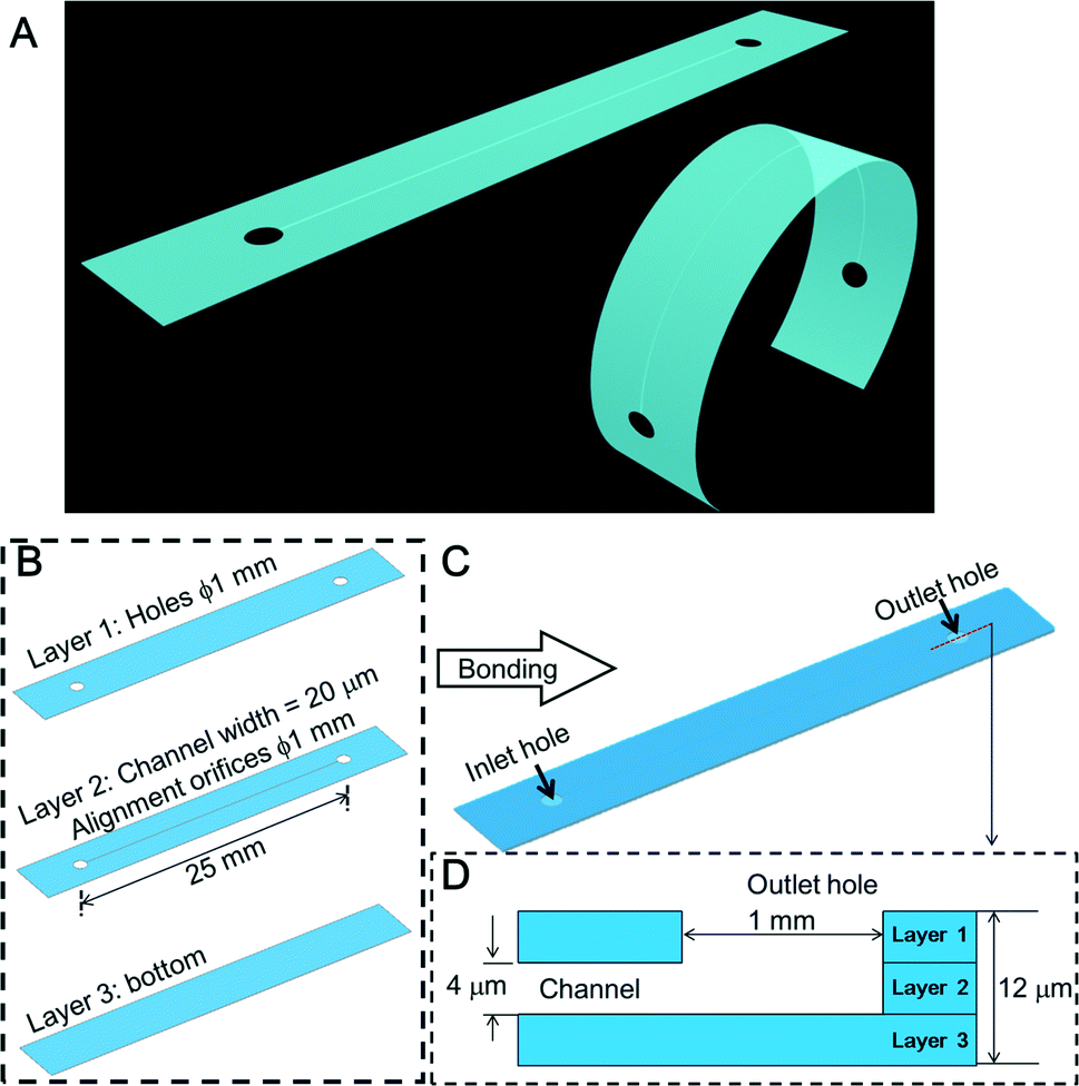 | ||
| Fig. 1 Schematic diagrams of ultra-thin glass microchip devices. (A) Concept image of the ultra-thin and flexible glass microchip device in extended and curled geometries. The total thickness is approximately 12 μm. (B) Design details of the three layers. (C) Bonding step to obtain the ultra-thin glass micro-fluidic device. (D) Cross-sectional view of the bonded device near the outlet. The thickness of each layer is 4 μm. | ||
Experimental
1. Preparation of materials
Ultra-thin glass sheets (size: 4 × 100 mm, 4 μm in thickness) were cut from a roll of ultra-thin glass sheet (OA-10G; available on rolls to 40 m length) (Nippon Electric Glass, Otsu, Japan). To prevent the glass sheets from sticking together, polymer sheets were placed between them, and the cut glass sheets were carefully stored.2. Micro-fabrication of glass sheets
The design of the ultra-thin glass chip is shown in Fig. 1B. The prototype chip consisted of three layers, each with an individual thickness of 4 μm. A micrometer-scale channel was fabricated in layer 2. Two orifices with a diameter of 1 mm were fabricated in both layers 1 and 2 for convenience of alignment. In layer 1, these orifices also served as the inlet and outlet. Layers 1, 2 and 3 were bonded together to form the prototype (Fig. 1C).The total thickness of the fully assembled prototype was estimated to be 12 μm (Fig. 1D). The fabrication process of layers 1 and 2 was done with a femtosecond laser (Solstice Ace100F; Spectra Physics, Santa Clara, CA). The laser wavelength was 800 nm, the pulse width was 100 fs, and the repetition rate was 1 kHz. Unlike other femtosecond laser processes for ordinary hard glass substrates, in the ultra-thin glass sheet process, focusing loss of the femtosecond laser was frequently observed, because the glass sheet was highly flexible and tended to curl slightly. To solve this problem, we forced the glass sheets for layers 1 and 2 into an extended and flat state by using silicone rubber on two sides and a simple homemade jig with a window (Fig. S1A†) when we were working on the sheets. The silicone rubber provided a handling zone for us to manipulate the glass sheets.
As another issue, much nano-debris was generated on the surface of the glass sheet after the femtosecond laser process (Fig. 2). Conventional laser micro-fabrication methods for glass substrates are done in a liquid medium to suppress the generation of nano-debris. However, in this study, we could not carry out the process in any liquid medium, because the shock wave due to the laser-induced breakdown can damage the glass sheets and the precise movement of the laser on the sheets is extremely difficult in liquid medium.30 Moreover, the debris generated from carrying out the laser fabrication in air might affect the quality of bonding. Therefore, to reduce the generation of nano-debris for obtaining a better surface condition, we investigated the optimal conditions of the laser pulse energy using two different objective lenses: a 20× lens (NA: 0.46) and a 40× lens (NA: 0.9). The energy of the beam was adjusted by a neutral density filter. The relationship between the width of the fabricated channel and the intensity of the laser pulse power is shown in Fig. 2. The widths at 10 points on a femtosecond laser-fabricated channel for different energy intensities were measured. The minimum laser pulse power to cut through the ultra-thin glass sheets with the minimum generation of nano-debris was selected to fabricate the prototype. The minimum width of the channel fabricated by a single cutting process with the optimized pulse energy was found to be approximately 0.7 μm.
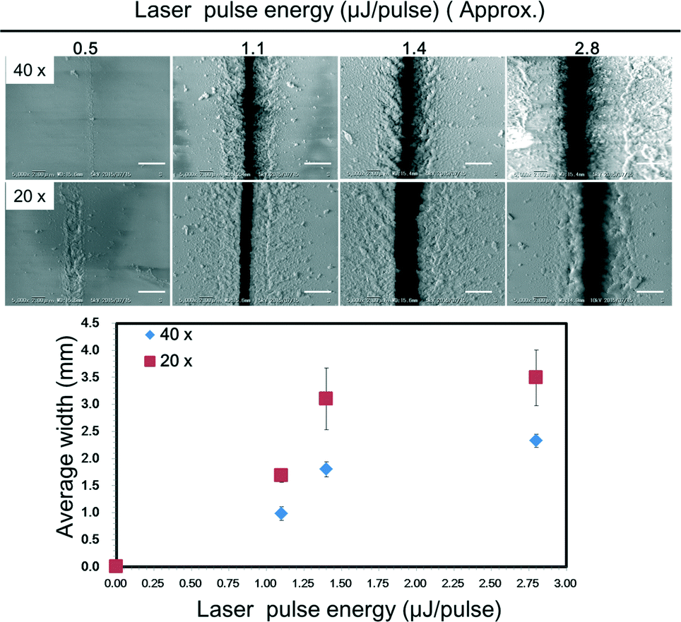 | ||
| Fig. 2 Laser pulse energy dependency of the fabricated channel width of the ultra-thin glass sheet obtained by femtosecond laser processing. The microphotographs show the microchannels made by the femtosecond laser on the ultra-thin glass sheet. They were obtained through a 40× or a 20× lens as a function of the laser pulse energy (0.5, 1.1, 1.4, and 2.8 μJ per pulse from left to right). Scale bars are 4 μm. The graph indicates the average widths of the channels as seen through the objective lens with magnifications of 40× (◆) and 20× (■). | ||
Then, using a programmable electromotive stage (BIOS-206T; Sigmakoki, Tokyo), a microscope (Olympus IX71; Olympus Inc. Tokyo), and the 40× objective lens, we fabricated the microchannel with a width of approximately 20 μm and a length of 25 mm in layer 2 as shown in Fig. S1B.† Details of the inlet are shown in Fig. S1C and D.† The inlet and outlet were fabricated in layer 1 by the same process. Making the orifices and channel of layers 1 and 2 took about 30 min. No fabrications were made in layer 3. Then, the ultra-thin glass sheets were released from the jig used to hold them in place during work.
Next, the ultra-thin glass sheets were chemically cleaned. In the cleaning process, a newly designed jig with a magnet fixture was used to hold each ultra-thin glass sheet (Fig. S2†). The jig was made of Teflon and glass and had several weak magnets. The silicone rubber with the ultra-thin glass was sandwiched by the magnet fixture on the jig. It was possible to chemically clean the three glass sheets at the same time.
The chemical cleaning process used piranha solution containing sulfuric acid and hydrogen peroxide at a ratio of 3![[thin space (1/6-em)]](https://www.rsc.org/images/entities/char_2009.gif) :1. Since highly cleaned surfaces are known to require no adhesive agent to bond to each other, we expected to be able to prepare an all-glass microchip with good flexibility and transparency of the channel. After 20 min of chemical cleaning, the glass sheets were slowly removed from the solution and rinsed with ultra-pure water for 10 min.
:1. Since highly cleaned surfaces are known to require no adhesive agent to bond to each other, we expected to be able to prepare an all-glass microchip with good flexibility and transparency of the channel. After 20 min of chemical cleaning, the glass sheets were slowly removed from the solution and rinsed with ultra-pure water for 10 min.
Next, the glass sheets were thoroughly dried with a nitrogen air gun (5 min) in a draft chamber. Layers 1 and 2 were exactly aligned by using a homemade jig (Fig. S3†). Careful cleaning ensured that they had no air or dust contamination. After that, the aligned layers 1–2 were manually placed on top of layer 3 and this was ready for fusion bonding.
For thermal fusion, the temporarily assembled chip was set in a programmable vacuum furnace (KDF-900GL; Denken, Kyoto, Japan). The chip was put on an alumina plate (40 × 80 × 5 mm) to prevent fusion to the bottom of the furnace, and 3 alumina plates as weights (75 × 65 × 5 mm; 300 g) were placed on the microchip to keep it flat before putting it into the furnace.
To prevent strain during cooling, which could degrade the flexibility of the ultra-thin glass, we used an optimized slow cooling process for the fusion bonding of the glass sheets.21 The conditions were: heating from 25 °C to 750 °C for 1.5 h; maintaining at 750 °C for 5 h; cooling from 750 °C to 700 °C for 2 h; maintaining at 700 °C for 30 min; cooling from 750 °C to 700 °C for 2 h; cooling from 700 °C to 650 °C for 1 h; cooling from 650 °C to 600 °C for 30 min; and finally cooling naturally by turning off the furnace. Then, we removed the alumina plate weights, took out the bonded ultra-thin glass chip, and carefully stored it between two polymer films (Fig. S4†).
3. Experimental setup
For investigating the basic functions of the ultra-thin and flexible glass micro-fluidic chip, a simple experimental system consisting of a pump and a microscope was prepared (Fig. S5A†). A flow rate programmable syringe pump (Fusion 200; Chemyx, Stafford, TX) was used. The inlet of the chip was connected to the pump with a silicon tube and a homemade metal jig31 (Fig. S5B†). The outlet was kept open. For monitoring the flow in the channel, fluorescent spherical polystyrene bead particles (Fluoro Spheres, 1 and 2 μm in diameter; Molecular Probes, Invitrogen, Carlsbad, CA) were dispersed into distilled water at a dilution of 1000×, and the water was used as the flow fluid. The flow was observed with a digital microscope (VHX-5000; Keyence, Osaka, Japan) and a lens (VH-Z100UR; Keyence); the lens was focused on the center of the microchannel (Fig. S5C†) and the flow images were recorded. The experiment was carried out at room temperature in a clean room.Results and discussion
1. Prototype of the ultra-thin glass micro-fluidic chip
We obtained the prototype ultra-thin and flexible glass chip shown in Fig. 3A. The fusion bonding process yielded a chip that was approximately 12 μm thick. To confirm the chip flexibility, the chip was bent more than 180 deg by pressing it with fingers; this is shown in the photographs of Fig. 3A–D and S6A,† which were taken from different viewpoints. The thickness profile of the chip at the channel was carefully inspected (Fig. 3E). The cross section of the channel was observed with a scanning electron microscope (SEM) (Fig. 3F), which showed that the thickness of the three layers was approximately 12 μm. Although Newton rings appeared in the glass micro-fluidic chip due to contaminating particles produced during fabrication, an unattached area or interference reflection of the three layers, bonding of the channel was confirmed from the SEM image (Fig. 3F) and also from the leakage test result in the following section. The three layers were firmly bonded at least in the areas near the channel. Bonding the three layers in an even cleaner environment or improving the method of applying a larger pressure could solve this problem.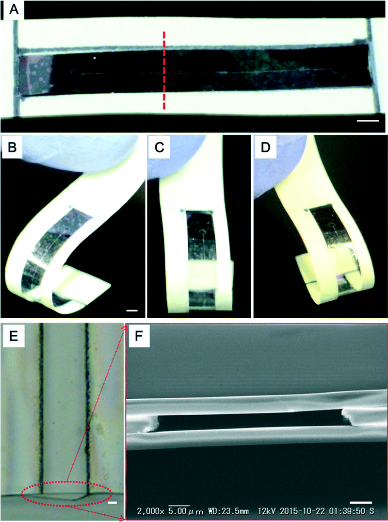 | ||
| Fig. 3 Prototype of the micro-fluidic chip. (A) Prototype micro-fluidic chip held on both sides by a paper holder. (B–D) The micro-fluidic chip with the holder could be bent by a finger while applying a slight pressure (blue) without breaking, indicating that the microchip had sufficient flexibility for handling. (E) Optical image of the cross-sectional area from the top side. (F) The SEM cross-sectional image of the glass micro-fluidic chip at the channel. Scale bars are 2 mm in (A) and (B) and 5 μm in (E) and (F). | ||
Although we saw no obvious influence from nano-debris near the channel, it would be desirable to have less nano-debris generation, and we suggest the use of a microscope system with an autofocusing function and conducting the fabrication process in a shallow solution environment as ways to do this.
The channel width was measured to be about 20 μm at various locations. In the area for laser focusing, the channel width was approximately 20 μm ± 10 μm. The reason for the deviation was that the glass sheet tended to curl slightly, which caused the laser to over-cut or under-cut the channel in the glass sheet.
The final weight calculated from the volume of the prototype chip (size: 30 mm × 4 mm × 12 μm) and the density (2.46 g cm−3)32 was approximately 3.6 mg.
2. Investigation of the function of the glass microchip
As a fluidic device, it is important to investigate the capacity of the microchannel of the chip to resist pressure.First, the microchannel was filled with water, and air was fed into it to inspect for possible leakage (Fig. 4A1–3) (Video S2†). As a result, no significant leakage was observed from the channel. Then, fluid containing 1 or 2 μm bead particles was fed into the channel, and their flow was observed at a flow rate of 30 μL min−1 (Fig. 4B1–3 and C1–3) (Videos S3 and S4†). The velocities of the beads clearly differed with the location in the channel and were from 67.32 to 167.11 μm s−1 (1 μm), and from 13.15 to 21.41 μm s−1 (2 μm). An increase in the flow rate over approximately 40 μL min−1 was found to break the bonding near the channel inlet area between layer 2 and layer 1. Because fluid leakage from the syringe and connectors was significant, the actual applied pressure to the channel was calculated to be 247.17–614.32 Pa from the motion data of the bead particles. The equations (Hagen–Poiseuille equation) were as follows.33
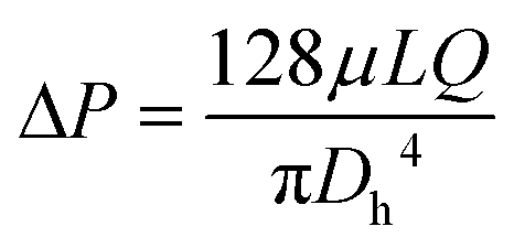
| (1) |

| (2) |
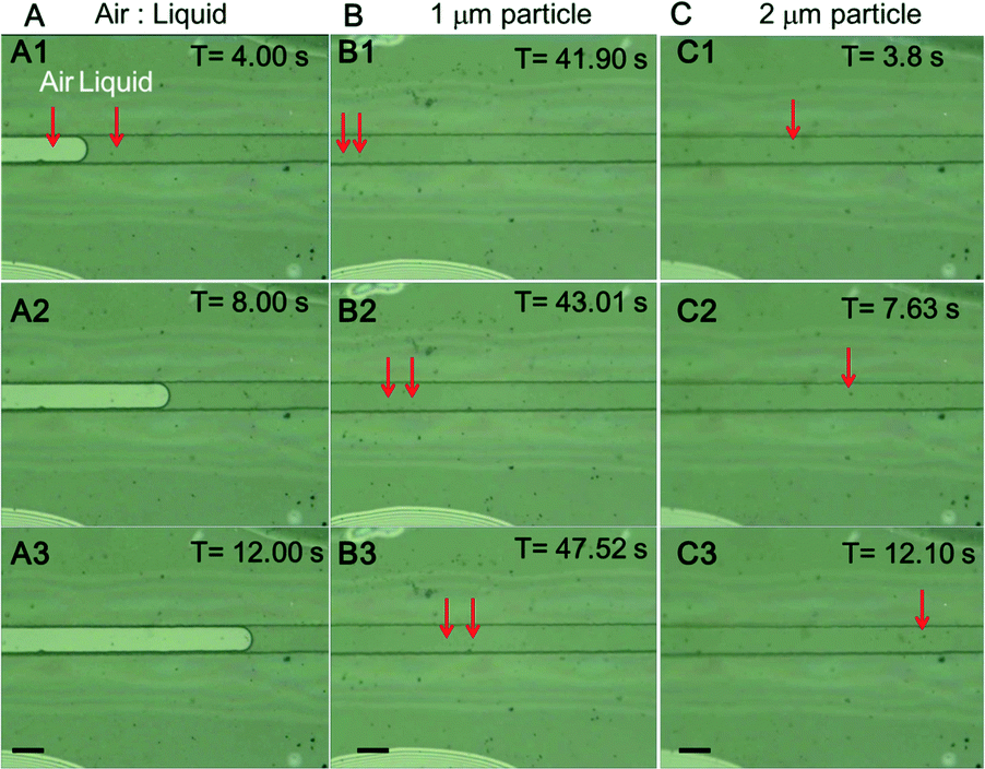 | ||
| Fig. 4 Fluid flow in the channel of the micro-fluidic chip. To investigate the chip function, the flow characteristics of the channel were observed. Photographs (A1–3) in the left column show the movement of the air and liquid interface. Photographs (B1–3) and (C1–3) in the middle and right columns show the movements of fluids containing particles with diameters of 1 and 2 μm, respectively. The black scale bars are 20 μm. | ||
In addition, a convenient connection of the ultra-thin glass chip was achieved by sandwiching it between a PDMS block with a reservoir and a thick glass plate (Fig. 5A and B). A solution of red dye was introduced into the channel to demonstrate the connection induced by capillary action (Fig. 5C). The flow of the solution was observed at the outlet (Fig. 5D1–3).
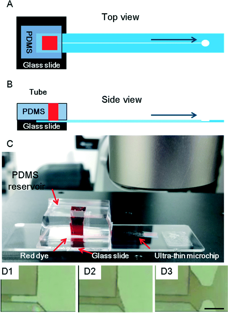 | ||
| Fig. 5 The interface for the ultra-thin glass connection. (A) and (B) are designs of the connecting interface. (C) The prototype ultra-thin glass micro-fluidic chip was connected with a PDMS reservoir filled with red dye. (D1–D3) The flow of the solution induced by capillary action was confirmed. The scale bar is 50 μm. | ||
3. The size of the microchip
For the purpose of drug delivery to a specifically small area, such as small-sized organs, a delivery device having a small size, good strength and chemical stability is required.For wearable and implantable medical devices, a lightweight and small-sized flexible substrate is useful. The sizes of the ultra-thin devices used in the above applications are from several tens of micrometers7,34 to several hundreds of micrometers.4 For high-resolution imaging, the cover glass with a thickness of 0.17 mm is generally used. Compared with the devices above, we were able to fabricate all-glass fluidic devices of approximately 12 μm thickness.
4. Comparison of the flexibility our chip with chips made with other materials
In this study, the bending curvature of the ultra-thin glass sheet was 0.5 mm, and the fracture toughness was over 400 MPa.32 We practically clarified the fragility of the three-layer micro-fluidic chip by a flexibility experiment in which we bent and twisted our chip in different directions (Fig. 6A). The bending curvature was less than 2 mm in the Y-direction (long axis) and 3 mm in the X-direction. The maximum twist degree was approximately 40° (Fig. 6B; Video S5†).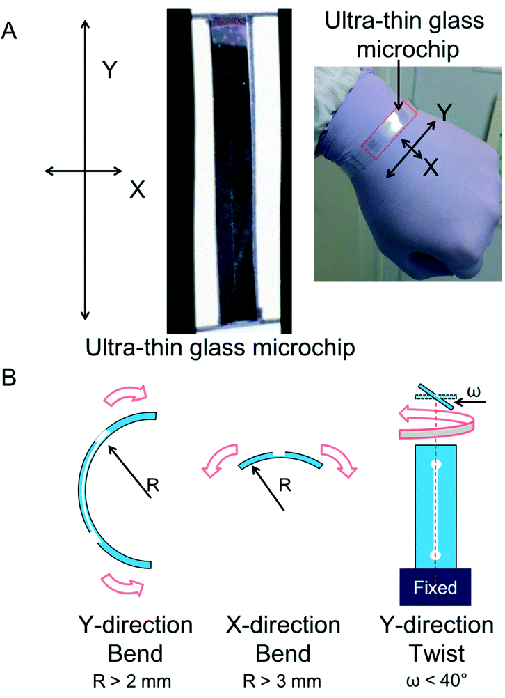 | ||
| Fig. 6 Confirmation of the flexibility. (A) For the Y-direction, the bending was along the long axis of the ultra-thin glass chip. For the X direction, the bending was along the short axis of the ultra-thin glass chip. (B) The bending curvature limit without breaking the chip was approximately 2 mm and 3 mm in the Y- and X-directions, respectively. The maximum degree of twisting was approximately 40° in the Y-direction. | ||
On the other hand, the most commonly found thin-glass devices are made from cover glasses. The thinnest flexible cover glasses, which are custom-made, have a minimum thickness of approximately 30 μm (NEO microscope cover glass; Matsunami Glass, Kishiwada, Osaka), and their bending curvature is 8 mm.
For further comparison, we also fabricated a thin PDMS chip by a conventional method (Fig. S3A†). According to the literature, the theoretical thickness limitation of pure PDMS is approximately 5 μm,35 and in that case, manually peeling off the PDMS from a substrate and handling the thin PDMS are extremely difficult tasks. The thickness of 100 μm is empirically suitable for manual handling. Therefore, we fabricated a PDMS chip consisting of two layers with a total thickness of 200 μm (Fig. S3B†). The flexibility (bending curvature: 1 mm) of PDMS with a thickness of 200 μm was better than that of the ultra-thin and flexible microchip. However, when fluid was fed into the 20 μm channel of the PDMS flexible chip, leakage was immediately found at the inlet at a flow rate of approximately 17 μL min−1, suggesting that the bonding strength between PDMS sheets36 was lower than that of thermal fusion-bonded glass sheets.37 In addition, most of the other flexible materials cannot be used for fabricating fluidic devices of less than 25 μm thickness such as polymers4 (>100 μm), paper10,11 (>70 μm), and plastics13,38 (>25 μm).
5. Investigation of the surface roughness of our microchip by optical measurement
Although normally wet etching methods for glass offer a higher fabricated surface quality, differences in the components of the etching solution and in target glasses mean the roughness of the fabricated glass material can become several tens of nanometers,26 although using post-processing treatments, such as oxygen/hydrogen flame polishing,39 annealing,40 and CO2 laser reflow,41 can reduce the roughness of the surface down to several nanometers. On the other hand, the roughness of the top and bottom surfaces of our microchip made by the thermal fusion bonding method was 0.5 nm.32 The quality of the surface ensures the transparency of the glass microchip.Moreover, because the thickness of the microchip from the surface to the channel is 4 μm, an extra working distance is available for optical research indicating a new possibility to design other useful devices. We also fabricated other flexible glass microchips with a different bonding method as a negative control. An ultra-thin glass sheet was coated with UV adhesive (GL-4007, 23 cp; Gluelabo, Kuwana, Mie) using a spin coater at 8000 rpm; the estimated layer thickness was <0.7 μm, as calculated from the density. The surface condition of the microchip made by the UV-adhesive bonding (Fig. S7A and B†) was rougher than that of the microchip made by the fusion bonding method (Fig. S7C and D†). The surface roughness was measured by using a 3-dimensional laser-scanning microscope (VK-8710, Keyence). The surface roughnesses of eight fusion-bonding samples and four UV-adhesive bonding samples were measured. The results indicated that the surface roughnesses clearly decreased from approximately 0.51 to 16.8 nm (Fig. S7E†). The UV-adhesive bonding method was judged to be unsuitable for fabricating ultra-thin microchips.
6. Investigation of the performance of the ultra-thin microchips for possible conventional applications
As a device made for convection-enhanced delivery, the thickness and weight of our fabricated micro-fluidic chip were thinner and lighter than those of microchips made using other methods. In addition, because the ultra-thin glass sheet is available on rolls at lengths up to 40 m, the tube, injector, and delivery structure can be integrated together with no dead volume in the flow line.Recently, in the field of wearable devices, flexible organic-based sensors and power devices have become popular. Most organic-based sensors and power devices have a low output power density due to several limitations of the materials used such as a low power factor, high contact resistance with a metal electrode, and low thickness for conduction materials.7 However, organic-based materials such as polymers are widely used for making flexible wearable devices that can be placed in contact with human skin safely. On the other hand, inorganic materials that can output a high power density are inflexible, and the device structure has to be carefully designed to obtain sufficient flexibility.7 With the method we described above, flexible and thin glass wearable devices, which have a high electrical-conducting character, good thermal conductivity,20 flexibility with a curvature of less than 2 mm, good chemical/physical stability, good transparency, and a long operating life, could be fabricated.
As an example, the use of a thin glass sheet is advantageous regarding the energy conversion efficiency for wearable power generators such as a thermoelectric (TE) power generator. A previous report used glass fabric (thickness of 20 μm) for a wearable TE power generator7 and it exhibited a higher output power density than other polymer materials. Also, the glass fabric layer with a 20 μm thickness has provided a TE device that is thin (<500 μm), lightweight (<0.13 g cm−2), and flexible. Our technology will provide wearable TE devices that are even thinner, lighter and more flexible.
Furthermore, methods for manual manipulation, handling, fabrication, cleaning, and bonding a 12 μm total glass device were also proved. Although we only fabricated a microchip with a simple design, the fabrication method was established and the potential of the ultra-thin glass microchip was confirmed. By simply changing or adding to the design and the fabrication process, various kinds of sensors, actuators, and structures can be fabricated.
Conclusions
This study investigated and established a method for fabricating an ultra-thin and flexible multi-layer glass micro-fluidic chip that was lightweight (3.6 mg) and thin (12 μm thick), and had a smooth surface (surface roughness of 0.5 nm) and high reusability. We investigated the optimized laser pulse power (1.1 μJ per pulse), selected an objective lens (40×) with a NA of 0.9, and determined the thickness of the ultra-thin glass (4 μm) for both effective fabrication and human handling of the microchip. The ultra-thin glass microchip will contribute to the advancement of various engineering and scientific fields including micro-measurement instrumentation, physical stimulation, clinical chemistry instrumentation, and biochemical analytical and synthesis fields. In addition, this report offered a basic method of fabricating and bonding ultra-thin glass devices for numerous applications. Our thinnest glass chip is a typical prototype for the demonstration of this method, because it includes the long distance cut-through, multiple layer alignment, and bonding processes.Acknowledgements
This research was funded by the ImPACT Program of the Council for Science, Technology and Innovation (Cabinet Office, Government of Japan).References
- I. Meyvantsson and D. J. Beebe, Annu. Rev. Anal. Chem., 2008, 1, 423–449 CrossRef CAS PubMed.
- S. Suresh, Acta Mater., 2007, 55, 3989–4014 CrossRef CAS.
- G. T. Roman, Y. Chen, P. Viberg, A. H. Culbertson and C. T. Culbertson, Anal. Bioanal. Chem., 2007, 387, 9–12 CrossRef CAS PubMed.
- C. P. Foley, N. Nishimura, K. B. Neeves, C. B. Schaffer and W. L. Olbricht, Biomed. Microdevices, 2009, 11, 915–924 CrossRef CAS PubMed.
- S. H. Kim, J.-H. Moon, J. H. Kim, S. M. Jeong and S.-H. Lee, Biomed. Eng. Lett., 2011, 1, 199–203 CrossRef.
- C. Pang, G.-Y. Lee, T. Kim, S. M. Kim, H. N. Kim, S.-H. Ahn and K.-Y. Suh, Nat. Mater., 2012, 11, 795–801 CrossRef CAS PubMed.
- S. J. Kim, J. H. We and B. J. Cho, Energy Environ. Sci., 2014, 7, 1959 CAS.
- F. C. Cheong, C. C. Wong, Y. Gao, M. H. Nai, Y. Cui, S. Park, L. J. Kenney and C. T. Lim, Biophys. J., 2015, 108, 1248–1256 CrossRef CAS PubMed.
- A. A. Epshteyn, S. Maher, A. J. Taylor, A. B. Holton, J. T. Borenstein and J. D. Cuiffi, Biomicrofluidics, 2011, 5, 1–6 CrossRef PubMed.
- A. W. Martinez, S. T. Phillips, G. M. Whitesides and E. Carrilho, Anal. Chem., 2010, 82, 3–10 CrossRef CAS PubMed.
- A. K. Yetisen, M. S. Akram and C. R. Lowe, Lab Chip, 2013, 13, 2210–2251 RSC.
- S.-Y. Cheng, S. Heilman, M. Wasserman, S. Archer, M. L. Shuler and M. Wu, Lab Chip, 2007, 7, 763 RSC.
- P. Hazarika, D. Chowdhury and A. Chattopadhyay, Lab Chip, 2003, 3, 128–131 RSC.
- J. Kuncová-Kallio and P. J. Kallio, Conf. Proc. IEEE Eng. Med. Biol. Soc., 2006, 1, 2486–2489 Search PubMed.
- A. Piruska, I. Nikcevic, S. H. Lee, C. Ahn, W. R. Heineman, P. A. Limbach and C. J. Seliskar, Lab Chip, 2005, 5, 1348–1354 RSC.
- H. Hisamoto, Y. Shimizu, K. Uchiyama, M. Tokeshi, Y. Kikutani, A. Hibara and T. Kitamori, Anal. Chem., 2003, 75, 350–354 CrossRef CAS PubMed.
- S. Hiki, K. Mawatari, A. Aota, M. Saito and T. Kitamori, Anal. Chem., 2011, 83, 5017–5022 CrossRef CAS PubMed.
- K. Jang, K. Sato, Y. Tanaka, Y. Xu, M. Sato, T. Nakajima, K. Mawatari, T. Konno, K. Ishihara and T. Kitamori, Lab Chip, 2010, 10, 1937–1945 RSC.
- K. Sugioka and Y. Cheng, Lab Chip, 2012, 12, 3576–3589 RSC.
- T. W. Tong, Thermal Conductivity 22, FL:CRC Press, Boca Rotan, 1994 Search PubMed.
- Y. Tanaka, RSC Adv., 2013, 3, 10213–10220 RSC.
- Y. Tanaka, K. Morishima, T. Shimizu, A. Kikuchi, M. Yamato, T. Okano and T. Kitamori, Lab Chip, 2006, 6, 362–368 RSC.
- Y. Tanaka, Micromachines, 2014, 5, 289–299 CrossRef.
- K. Jang, Y. Xu, K. Sato, Y. Tanaka, K. Mawatari and T. Kitamori, Microchim. Acta, 2012, 179, 49–55 CrossRef CAS.
- Y. Tanaka, in Micro Total Analysis Systems 2014, 2014, vol. 2, pp. 1683–1685 Search PubMed.
- C. Iliescu, K. L. Tan, F. E. H. Tay and J. Miao, Proc ICMAT 2005 Symp. F Singapore, 2005, vol. 44, pp. 75–78 Search PubMed.
- H. Huang, L. M. Yang and J. Liu, Nanophotonics and Macrophotonics for Space Environments V, Proc. SPIE 8164, 2011, p. 81640B Search PubMed.
- F. He, Y. Liao, J. Lin, J. Song, L. Qiao, Y. Cheng and K. Sugioka, Sensors, 2014, 14, 19402–19440 CrossRef CAS PubMed.
- Y. Liao, Y. Shen, L. Qiao, D. Chen, Y. Cheng, K. Sugioka and K. Midorikawa, Opt. Lett., 2013, 38, 187–189 CrossRef CAS PubMed.
- Y. Hosokawa, H. Masuhara and T. Kaji, Three-dimensional analysis of tightly focused femtosecond laser beam and shockwave propagations in water, Proc. International Journal of Optomechatronics, 2011, pp. 123–126 Search PubMed.
- Y. Tanaka, H. Xi, K. Sato, K. Mawatari, B. Renberg, M. Nilsson and T. Kitamori, Anal. Chem., 2011, 83, 3352–3357 CrossRef CAS PubMed.
- Nippon Electric Glass Manufacturer's Catalogue for Products Glass-Ribbon, Available online: http://www.neg.co.jp/en/product/ep/glass-ribbon (accessed on 1, Dec, 2015) Search PubMed.
- H. Bruus, Theoretical Microfluidics, Oxford University Press, Oxford, UK, 2008, pp. 65–68 Search PubMed.
- S. Cosson, L. G. Aeberli, N. Brandenberg and M. P. Lutolf, Lab Chip, 2015, 15, 72–76 RSC.
- J. H. Koschwanez, R. H. Carlson and D. R. Meldrum, PLoS One, 2009, 4, 2–6 Search PubMed.
- M. A. Eddings, M. A. Johnson and B. K. Gale, J. Micromech. Microeng., 2008, 18, 067001 CrossRef.
- M. M. R. Howlader, S. Suehara and T. Suga, Sens. Actuators, A, 2006, 127, 31–36 CrossRef CAS.
- M. Focke, D. Kosse, C. Müller, H. Reinecke, R. Zengerle and F. von Stetten, Lab Chip, 2010, 10, 1365–1386 RSC.
- F. He, Y. Cheng, Z. Xu, Y. Liao, J. Xu, H. Sun, C. Wang, Z. Zhou, K. Sugioka, K. Midorikawa, Y. Xu and X. Chen, Opt. Lett., 2010, 35, 282–284 CrossRef CAS PubMed.
- F. He, J. Lin and Y. Cheng, Appl. Phys. B: Lasers Opt., 2011, 105, 379–384 CrossRef CAS.
- J. Lin, S. Yu, Y. Ma, W. Fang, F. He, L. Qiao, L. Tong, Y. Cheng and Z. Xu, Opt. Express, 2012, 20, 10212–10217 CrossRef CAS PubMed.
Footnote |
| † Electronic supplementary information (ESI) available. See DOI: 10.1039/c6lc00132g |
| This journal is © The Royal Society of Chemistry 2016 |