
 Open Access Article
 This Open Access Article is licensed under a Creative Commons Attribution-Non Commercial 3.0 Unported Licence
A microfluidic opto-caloric switch for sorting of particles by using 3D-hydrodynamic focusing based on SLE fabrication capabilities†
G.
Meineke
*a,
M.
Hermans
*b,
J.
Klos
a,
A.
Lenenbach
*a and
R.
Noll
a
aFraunhofer Institute for Laser Technology ILT, Steinbachstraße 15, 52074 Aachen, Germany. E-mail: Georg.Meineke@ilt.fraunhofer.de; Achim.Lenenbach@ilt.fraunhofer.de; Reinhard.Noll@ilt.fraunhofer.de
bLightFab GmbH, Steinbachstraße 15, 52074 Aachen, Germany. E-mail: m.hermans@lightfab.de
First published on 26th January 2016
Abstract
In a miniaturised flow switch fluid flows are controlled by reducing the local viscosity via absorption of laser radiation. Through this, the local flow rates are increased to switch the outlet port of a fluid flow carrying the analyte. The microfluidic chip is fabricated using Selective Laser-Induced Etching (SLE). SLE allows novel 3D-hydrodynamic focusing, realising circular shaped channel cross-sections and adapting interaction volume geometries to the profile of the laser radiation for optimised absorption. The performance of the switch is validated experimentally with a dyed analyte and video image processing. The ability to sort particles like cells is demonstrated at 8 Hz using polystyrene beads having a diameter of 8 μm.
Introduction
Microfluidic switching
In the field of applications for microfluidic devices, an important area is the selection and separation of single particles as e.g. drops or cells, within a mixture of other particles. Mostly known as micro total analysis systems (μTAS) or micro fluorescence-activated cell sorter (μFACS), different methods for driving the sorters have been proposed and demonstrated. The methods can be categorised into electrokinetic mechanisms, acoustophoresis, mechanical systems and optical manipulations.1 Implementing the functionality of sorting in a microfluidic chip usually increases the complexity of the set-up and the manufacturing of the chip and, with it, the cost. The methods in the first three categories need the most complex chips, because of integrated electrodes, mechanics, piezoelectric actuators, additional channels and ports. The fourth approach, optical manipulations, can be implemented with a simple microfluidic structure with four fluid ports, two inlets for analyte and sheath flows and two outlets for waste and collection flows. Additional ports can be limited to optical ports, for example an optical system for fluorescence excitation and detection and a second port for driving the switch. Demonstrated laser driven μFACS deployed optical scattering and gradient forces,2–9 creation of cavitation bubbles10,11 or sol–gel deformation.12,13 The use of optical scattering and gradient forces needs complex set-ups with sophisticated optics and challenging adjustments of the laser beams because of the small foci where the forces are applied. Channel filling interference patterns,7 moving laser foci4–6 or multiple laser beams2 are employed to prolong the interaction time between the laser beam and the particle. In the cases of sol–gel deformation and cavitation bubble generation, the laser foci position is less critical, therefore the set-up can be less complex, but the chip needs to have two more ports and handling of one extra fluid is required.Hence, for future applications a new method reducing the complexity of the system would be interesting with cheaper chips and a less complex periphery.
Hydrodynamic focusing
Besides the method for driving the switch, another key functionality in μFACS is hydrodynamic focusing. By merging the analyte channel with the surrounding buffer-conducting channel, the analyte flow is sheathed by a buffer solution in the middle of the channel and can be narrowed down to a smaller cross section with marginal mixing with the sheath flow due to the characteristics of laminar flow. This method allows to control the position and cross section of the analyte flow in a scale of a few micrometres. Moreover this reduces the risk of multiple particles passing the detection volume at the same time and makes it easier to switch the analyte flow from the waste channel to the collection channel. The analytes are confined most often in 2D, i.e. the sheath flow focuses the analyte flow in one direction, typically the horizontal one.11,12,14–22 This is because of the applied lithographic methods which allow fabrication of planar structures with one global depth, but the application of these methods gets more challenging and complex for structures with changing depths or crossing channels. Changing depths are most often generated by multistep lithography and crossing channels by building sandwich structures of several planar microfluidic layers.23 3D-focusing in two directions, horizontally and vertically, was demonstrated using multi-layered microfluidics,24,25 a chimney structure,26 step structures27,28 or chevron shaped structures29 on the floor of the channel and also by use of centrifugal forces in the curved channels.30 These methods for focusing need complex multistep manufacturing techniques and are sensitive to flow variations or focus the analyte flow excentrically31 with a non-circular shape. By using femtosecond-pulsed laser irradiation 3D-freeform microfluidic channels can be manufactured. With this approach a 3D hydrodynamic focusing was demonstrated by Paiè et al. enclosing the analyte flow by four surrounding sheath flows.32Manufacturing 3D microfluidic networks
In microfluidic networks with channels positioned at different separated layers (2.5D), the complexity of microfluidic systems can be dramatically more compared to 2D microfluidics. This is because of connections between the arbitrarily separated areas of the chip, without 2D routing restrictions or the need for external chip connections. 2.5D microfluidics are manufactured by stacking 2D microfluidic layers made of PDMS27 (polydimethylsiloxane, a silicon based organic polymer), repetitive stacking and structuring of a photosensitive SU-8 layer34 or laminating layers of polyimide and silicon.35 These manufacturing methods use bonding and stacking processes with high requirements regarding the positioning of each layer and the cleanness during stacking. Consequently, assembly is often considered to be the most expensive step in microsystem processes.36 A further method for manufacturing 2.5D microfluidic networks is by using a polymer as sacrificial layers with lithographic structuring, covering the structures with silicon or silicon nitride films, repetition of these steps for each 2D layer and finally removing the sacrificial layer by chemical dissolution or thermal decomposition.37 Even though 2.5D microfluidic networks are enabling more complex systems, the key elements remain in 2D like the hydrodynamic focusing section (with a few exceptions24–26).For the generation of 3D microfluidic networks there were several methods demonstrated including femtosecond laser direct writing, microstereolithography and selective laser-induced etching (SLE). Femtosecond laser direct writing is a two-step process: first the fluidic network is created by femtosecond laser ablation within a mesoporous glass substrate and secondly the pores are closed by annealing. Through this method the fabrication of a 3D microfluidic mixer has been demonstrated.38 Writing speeds of 10–100 μm s−1 were achieved and after 4 repetitive exposures the 3D microchannel was machined into the glass. During the annealing step the mesoporous glass substrate shrinks ∼40% in volume. With microstereolithography, a liquid photoresist is polymerised level by level, building complex objects using models set-up with computer-aided design (CAD) software. Through this approach, microfluidic chips39 and microfluidic components like valves40 with features as small as 50 μm have been manufactured. The polymerization process makes the use of an absorber and photoinitiators necessary. These substances are partially toxic and need certification for new applications in biomedical technologies.
SLE is a two-step bulk machining process in which the volume in a transparent substrate is first exposed by pulsed laser irradiation and secondly removed by wet-chemical etching. Using this method a monolithic cell counter with 3D hydrodynamic focusing was fabricated by Paiè.3 The smallest channel diameter shown by Paiè was 50 μm. For the reason of chemical, thermal and mechanical resistance as well as optical transparency along with low autofluorescence, thus a high degree of biocompatibility, glass is the material chosen to be suitable for the present application. In order to machine 3D microchannel systems within glass, SLE is used due to a higher productivity in comparison to fs laser direct writing within mesoporous glass. SLE is demonstrated with single exposures at writing speeds up to 200 mm s−1 and even several meters per second.
Working principle and experimental set-up
Microfluidic chip design
Here we present a method for microfluidic switching using a simple chip design with four ports, two inlet ports for the analyte and sheath flows and two outlet ports for the waste and the collection flows. Fig. 1 shows a photo of the chip with a blue analyte flow. The chip is manufactured monolithically from fused silica by Selective Laser-Induced Etching (SLE) described below. By injecting the analyte flow in the middle of two kidney-shaped sheath flows, 3D hydrodynamic focusing is realised by vertical and horizontal confinement near the middle of the channel. The initial position of the focused analyte flow is determined by two narrow sections I and II at an upstream position in the sheath flow channels with high hydrodynamic resistances RI and RII, see Fig. 2. Section II is designed 14% longer than section I, such that the difference in the resistances of RI and RII causes the flow rate QI to be larger than QII by default. Due to the larger QI, the initial position of the analyte flow is shifted towards the negative y-direction which forms the non-switched state as is depicted in Fig. 2(a). The narrow sections are folded two times in the z-direction forming a wide S-shape for optimised radiant flux absorption described below and have a cross section in the yz-plane of 30 μm × 100 μm, cf.Fig. 2(c). At a subsequent Y-fork the flow is divided in approximately equal parts into the collection and the waste flows.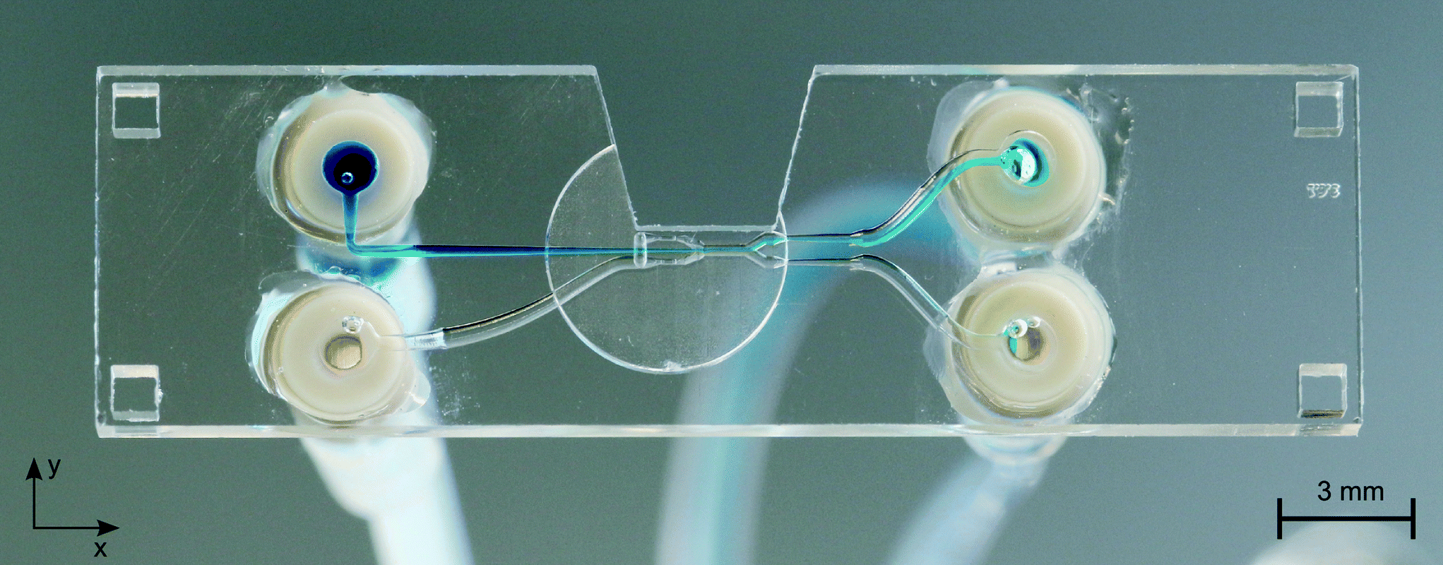 | ||
| Fig. 1 Photo of the microfluidic chip with a blue dyed analyte. | ||
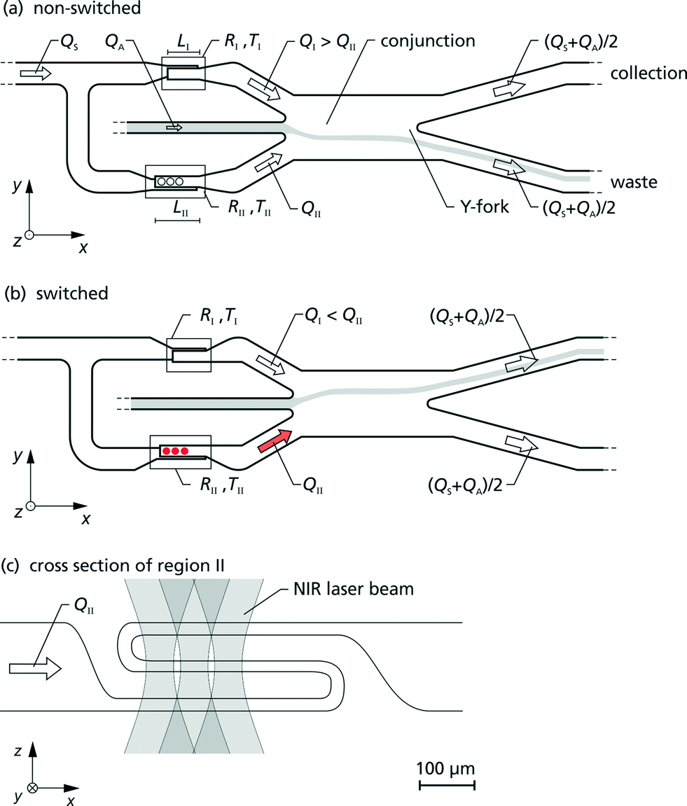 | ||
| Fig. 2 Schematic design of the opto-caloric switch for microfluidic sorting: two narrow sections (marked by rectangles), one in each sheath flow feed, define the ratio between the sheath flow rates QI and QII. The lengths of the narrow parts are different, with LI < LII such that, due to the hydrodynamic resistances RI and RII, in the unswitched state (a) QI > QII is sufficient to deflect the analyte flow QA into the waste channel. In the switched state (b) the temperature TII is increased such that QI < QII and the analyte flow is deflected into the collection channel. The narrow sections are folded two times in the z-direction forming a wide S-shape (c) for optimised radiant flux absorption. The circles inside the narrow section II illustrate the positions of the laser beams irradiating this section to initiate switching. | ||
Opto-caloric switch
Schulz et al. demonstrated in 1998 the possibility to switch an analyte flow by heating one of two sheath flow channels using electric current.19 Our new approach is to heat the sheath fluid directly by laser irradiation. In Fig. 2 the working principle is illustrated.By direct heating of the sheath fluid in section II with laser radiation, the hydrodynamic resistance RII is transiently decreased because of the lower viscosity of water at an elevated temperature. With decreasing resistance RII the hydrodynamic focusing is shifted towards the positive y-direction. If the resistance RII is sufficiently decreased below RI, then the hydrodynamically focused analyte flow exits the chip completely in the collection flow. This forms the switched state as is shown in Fig. 2(b).
Due to the absorption by water, the temperature rises directly in the channel without need for heat conduction by the surrounding chip material, allowing fast response of the system. Typical transition times of the sheath fluid through this narrow section are from 0.2 ms to 2 ms, giving a characteristic time scale.
The opto-caloric switch shifts the whole analyte flow. Combined with an optical sensor – such as forward scattering, sideward scattering or a fluorescence sensor – a sorter can be achieved, in which the shape, size and other physical properties like ductility of the particles have no significant effect on the sorting results, as long as the particles move along with the flow. This is a benefit compared to sorter concepts which utilise electrokinetic mechanisms, acoustophoresis, optical scattering or optical gradient forces for actuation.
Because of the distance between the heated narrow sections and the conjunction and because of the relatively long heating pulses, only minor pressure and temperature gradients at the particle path are exerted, compared to other, faster opto-caloric sorter concepts, for instance the one presented by Chen and Wu.10,11 Hence we expect that our sorter concept is less stressful for living cells. This will also result to longer switching times, which will result in lower throughput or lower downstream purity compared to faster opto-caloric sorter concepts.
Experimental set-up
Fig. 3 illustrates the experimental set-up. Two syringe pumps (neMESYS V2, Cetoni GmbH) drive the analyte and the sheath fluid into the chip. The chip is made of fused silica, which is transparent to NIR radiation used for heating. From two outlets the fluids are stored separately in a waste vessel and a collection vessel. A video camera with a microscope objective monitors the microfluidic switch.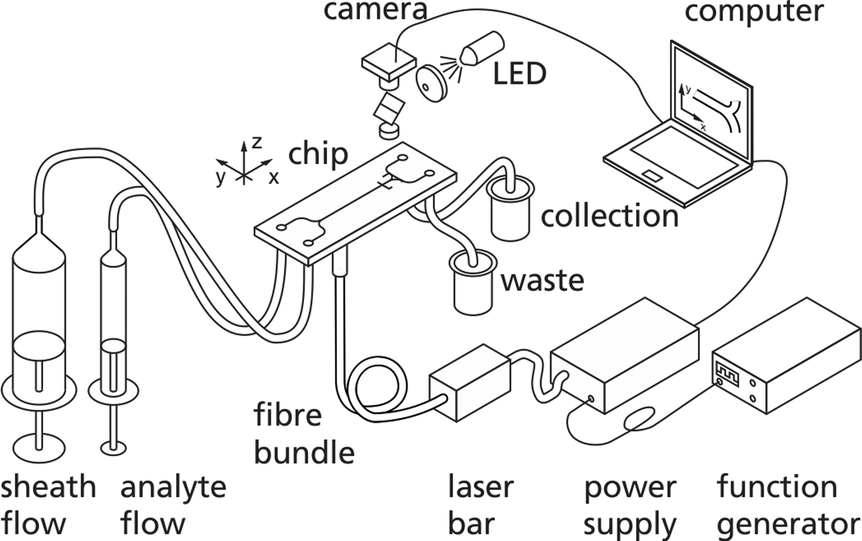 | ||
| Fig. 3 Schematic layout of the experimental set-up. | ||
Optical set-up
For heating of the narrow section of the chip, cf.Fig. 2(c), we use a multi-emitter laser module based on a 20-emitter AlGaIn/AsSb-laser bar (m2k-laser GmbH). Every second emitter is coupled into one multimode fibre with a core diameter of 105 μm and is separately supplied by an output stage of a multi-channel power supply (Amtron GmbH).Seven fibres are combined to a fibre bundle and the tips are glued into one ferrule. By using two consecutive gradient index lenses the seven fibre tips are imaged into the chip. For heating, three of the seven fibres are used; the positions of the laser foci in region II are marked in Fig. 2(a) and (b) by circles. The irradiated area of the chip is 11.780 μm2 which allows robust alignment.
Methods
Microfluidic channel fabrication
The 3D microfluidic chips described here are produced by selective laser-induced etching (SLE). SLE is a two-step process. In the first step ultra-short pulsed laser radiation is focused on a micrometre-sized spot and the focal spot is placed into a material which is transparent to the wavelength of laser radiation. If the laser irradiation in the vicinity of the focal spot exceeds the threshold for non-linear ionisation effects the absorption of light generates free-carrier electrons in the conduction band of the material.33 After some picoseconds, the energy is transferred from the excited electron system to the atoms and the solid is heated up to a temperature of several thousand Kelvin.41 The focal spot is moved in a linear way through the material and thus the material is rapidly quenched. By these processes of heating and quenching, a permanent modification is being scribed into the material. This laser modification is accomplished without cracks and with a precision better than ±1 μm. An arbitrary volume connected in three dimensions is exposed inside the glass by 3D scanning of the laser focus. In the second step of developing only the modified material is removed by wet-chemical etching starting at the surface of the workpiece. For precision of the SLE technique the selectivity is essential. The selectivity is the ratio of the etching rate of the modified material and the etching rate of the untreated material and is a quantity used to evaluate the aspect ratio of the geometries that can be generated with SLE. The observed selectivities differ for the materials investigated so far. While for sapphire and fused silica the maximum selectivities are >1000,42 newest results from LightFab show that also for soda-lime, Borofloat 33 and ULE (ultra-low expansion) glass, selectivities can be greater than 300. With selectivities in this range, complex 3D cavities and channel systems can be produced using SLE. The basis for this is filling a volume by juxtaposing single lines, which then will be removed after etching. The SLE machining capabilities range from precision micro holes for filtering or optical applications to complex pre-mounted mechanical drives with a precision of up to ±1 μm and a surface roughness of Rz down to ∼1 μm.For the microfluidic chip presented here the data for the linear scanning of the laser focus are derived automatically from a 3D-CAD model of the chip similar to the common procedure in 3D printing. The model is sliced into layers and the generated contour lines are filled with hatch vectors to irradiate all the materials which are intended to be leached out after etching. The data are transferred to the machine used for the laser inscription machine (Microscanner, LightFab with Satsuma Laser, Amplitude Systems). The lines are inscribed into a 2 mm thick fused silica wafer (SK1300, Ohara Corp.) at a wavelength of 1030 nm and an average optical power of 250 mW. After 4 days of etching in an 8 mol L−1 KOH solution the ready-to-use chips fall out of the wafers.
Heating by laser irradiation
The radiant flux emitted by each fibre can be controlled independently and reaches a maximum of more than 510 mW. The wavelength varies depending on the radiant flux used – between 1910 nm and 1940 nm – and matches an absorption band of water at 1930 nm as is shown in Fig. 4. For biocompatibility we investigated the absorption of saline. Using phosphate buffered saline with Tween 20 (PBST) prepared from a concentrated stock solution (Roti-Stock 10X PBST, Roth) and deionised water, no significant change in absorption is found.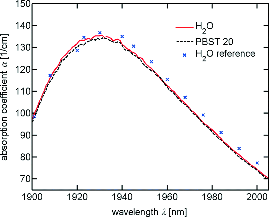 | ||
| Fig. 4 Absorption of water and PBST at wavelengths between 1900 nm and 2000 nm. Absorption is measured using a UV/VIS/NIR spectrophotometer (Lambda 1050, PerkinElmer) using cuvettes with thicknesses of 0.01 cm and 0.02 cm and calculating the geometric means of 4 (H2O, solid line) and 3 (PBST, dashed line) measurements, respectively. For the measurements of H2O, deionised water is employed. The reference data are taken from Kou et al.43 (crosses). | ||
The heated narrow section is designed using a flat channel which is folded two times in the z-direction in a way that the laser irradiation passes the height of the channel (40 μm) three times, resulting in an absorption of about 83% of the radiant flux.
Switch performance characterisation
The switch dynamic is characterised by taking images of the dyed analyte flow at the conjunction area and the Y-fork. 500 images are taken with a repetition rate ranging between 125 and 250 Hz, each image is saved with a millisecond resolved time-stamp. Laser switching is controlled by periodic TTL signals produced by a function generator (SFG-2120, GW Instek). The laser power follows a rectangular signal with frequencies from 8 Hz to 200 Hz and duty cycles from 40% to 60%. Improving the contrast of the analyte flow is accomplished by subtracting an image of the same section without dye. The analyte flow position is determined by fitting a Gaussian curve to the grey levels of the images along a line depicted in Fig. 5 as the y-axis. Using the time-stamp each image is saved, we increase the sampling time by sorting the images in a stroboscopic manner.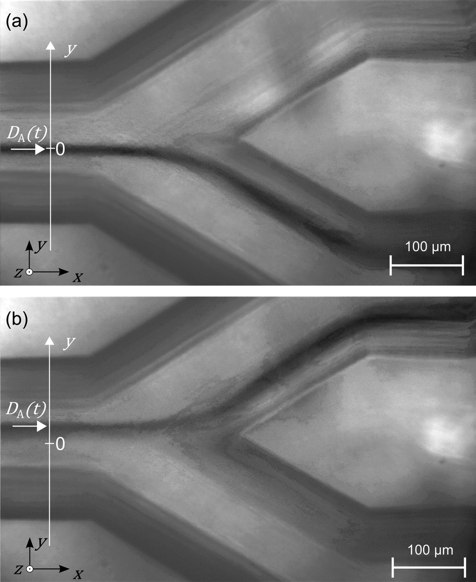 | ||
| Fig. 5 Microscopy image of the (a) non-switched and (b) switched states. The analyte flow is visualised by dying with patent blue V. The contrast is enhanced using reference images without dyed flow. The performance of the switch is quantified by determination of the lateral y-position of the analyte flow indicated by the white arrow. | ||
The switch response time τ is determined by fitting an exponential saturation curve to the rising edge of the dyed analyte flow position, with the maximum displacement D∞.
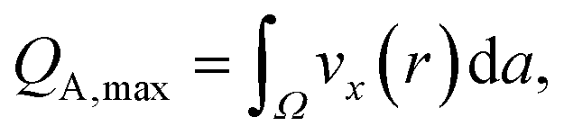
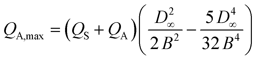
The maximum amount of analyte flow QA,max which can be switched is estimated by determination of the maximum displacement D∞ of the dyed analyte flow and comparison with the total flow rate. The quantity QA,max can be estimated by integrating the cross-sectional area Ω the analyte flow could cover at the maximum displacement D∞ without exceeding the dividing line of the Y-fork at the middle of the channel (cf. dashed vertical line in Fig. 6), weighted with the parabolic velocity field of a laminar flow, see Fig. 6(b):
 | (1) |
 | (2) |
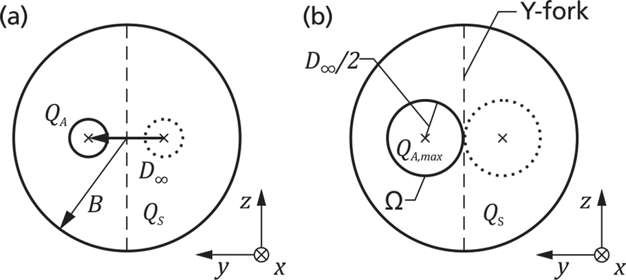 | ||
| Fig. 6 Diagram which illustrates the estimation of the maximum switchable amount of analyte flow QA,max. In (a) the situation of the experiment is shown to determine D∞ and in (b) the limiting case for a maximum analyte flow QA,max is shown. The non-switched position is drawn as a dashed circle, the switched state as a solid circle. B is the radius of the channel cross section, D∞ the analyte displacement, QS the sheath flow rate, QA the dyed analyte flow rate, and Ω the cross-sectional area covered by the switchable amount of analyte flow. | ||
The assumption of a parabolic velocity field is a simplification. In the experiment, especially at the conjunction where the flows combine, deviations from this assumption will occur. As a result of this, in the experiment, the observed QA,max values are higher than the estimated values by up to two.
Switching particles
The features of switching a flow of particles are tested using microbeads as the analyte sample. The particles are made up of polystyrene and have diameters of about 8 μm. The images are taken with repetition rates from 55 Hz to 220 Hz and sorted using time-stamps. By subtraction of a mean image, built from the preceding and the succeeding images, the particle contrast is enhanced. Using a threshold, a binary image is generated and single beads are identified and their location (xi, yi) is determined by identifying the largest connected area big enough to be formed by a bead. The time tc at which a bead passes the position at the left edge of the microscopy image in Fig. 5 is calculated as tc = ti − xi/v using the time-stamp of the image ti, the mean velocity of the flow ν and the observed x-position of the particle, xi. Depending on the y-position (yi) of the identified particle, it is classified as positive (switched) or negative (non-switched). In Fig. 7 a further classification scheme is depicted. Using the time tc of the beads and the state of the switch, the particles are classified as: I) true-positive, if they are positive and the switch is on, II) false-positive, if they are positive and the switch is off, III) false-negative, if they are negative and the switch is on and IV) true-negative, if they are negative and the switch is off. The switch is considered as being in the status on from 6 ms after the laser is switched on until the laser is switched off, cf. double arrow in Fig. 7. For each set of parameters we took three series of 500 images each. At frequencies greater than 8 Hz, the time assignment of the particles deteriorates due to increased errors caused by varying particle velocities especially after the Y-fork for particles near the inner channel wall.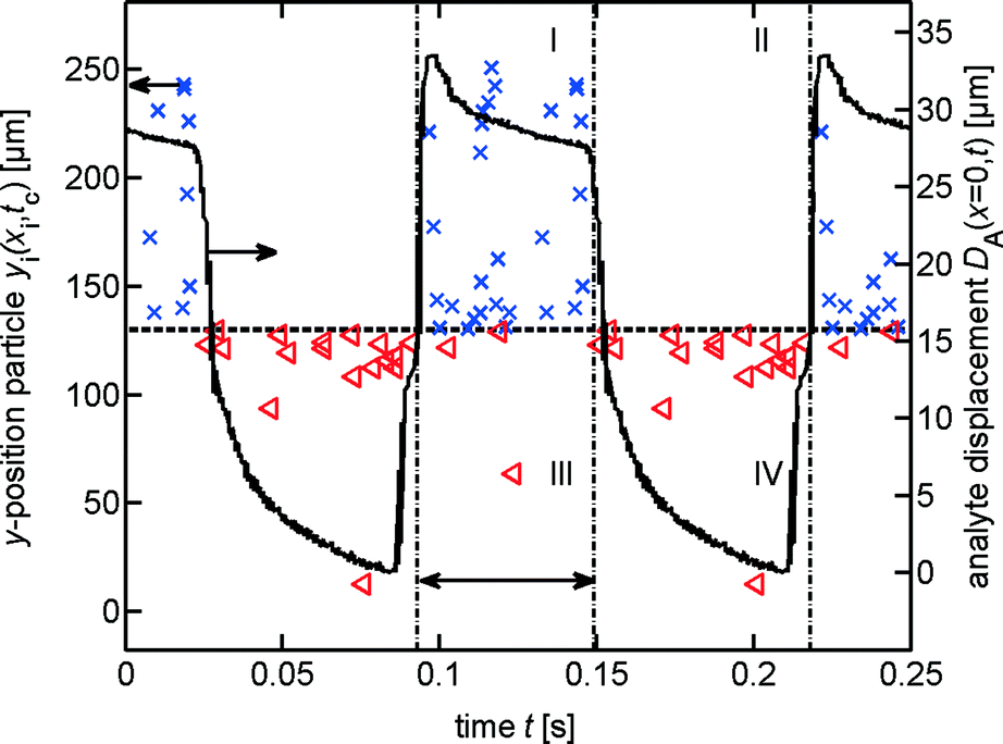 | ||
| Fig. 7 Time resolved particle position and classification of particles. By depicting the y-positions of the particles at the time tc, the ability to switch particles is estimated. If the y-position is longer than the centre of the Y-fork, plotted as a dashed horizontal line, the particles are considered as switched and depicted as crosses. For y-positions smaller than the centre of the Y-fork, the particles are considered as non-switched and depicted as triangles. The particles are classified according to the state of the switch and the y-position. The conditions for the classification are represented by four areas: I) true-positive, II) false-positive, III) false-negative and IV) true-negative. The data shown are taken with QS = 200 μl min−1 and QA = 5 μl min−1 at a switching frequency of 8 Hz. For the same set of parameters the displacement DA of the dyed analyte is plotted as a solid black line, illustrating the dynamics of the switch. The data in the time interval (0, 0.125 s) are copied to the interval (1.25 s, 0.250 s) to illustrate two full switching cycles. | ||
Results and discussion
3D microfluidic features
By positioning the finest structures of the microfluidic network in the middle of the chip, the leachate reaches these parts last, which preserves the fine details. In Fig. 8 microscopy images from (b) the top (minus z-direction) and (c) from the side (minus y-direction) are seen. The 3D hydrodynamic focusing is visible as the blue analyte stream narrows down at the conjunction in the y-direction (as is seen in (b)) and also narrows down in the z-direction (as is seen in c). In Fig. 8(c) also one folded narrow section with three levels is visible. The height of the middle level forms the narrowest part of the microfluidic device having a channel height of 40 μm. This shows the strength of SLE in manufacturing microfluidic systems with narrow parts, channels on multiple levels and a combination of different channel diameters and differently shaped cross sections. The manufacturing process is still simple and does not require any assembly steps.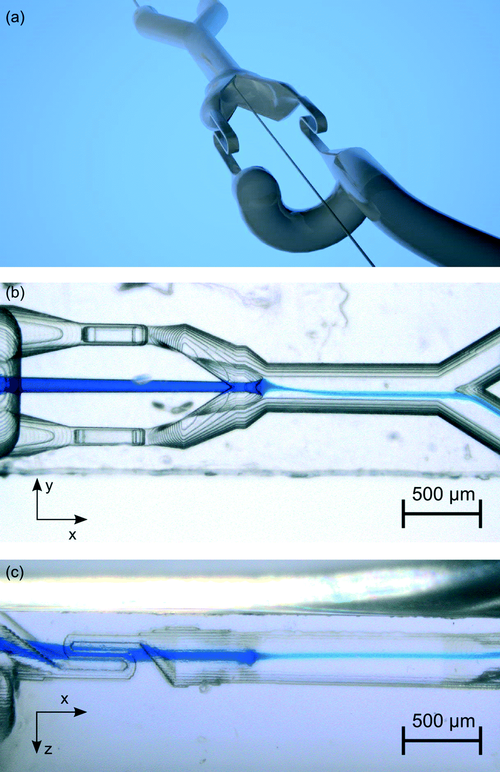 | ||
| Fig. 8 Microfluidic network (a) as computer generated image and (b) top view (minus z-direction) and (c) side view (minus y-direction) of the microfluidic chip with the blue analyte. The microscopy images are taken at a sheath flow of 200 μl min−1 and an analyte flow of 5 μl min−1. | ||
Switch response time
We investigated the response time for the different sheath flow rates and observed a decrease with an increasing flow rate, see Fig. 9. At a sheath flow rate of 50 μl min−1 the response time is determined to be (30.0 ± 0.5) ms. With increasing sheath flow rates the response time decreases to (20 ± 5) ms at 100 μl min−1, (7 ± 3) ms at 200 μl min−1 and (5 ± 2) ms at 400 μl min−1.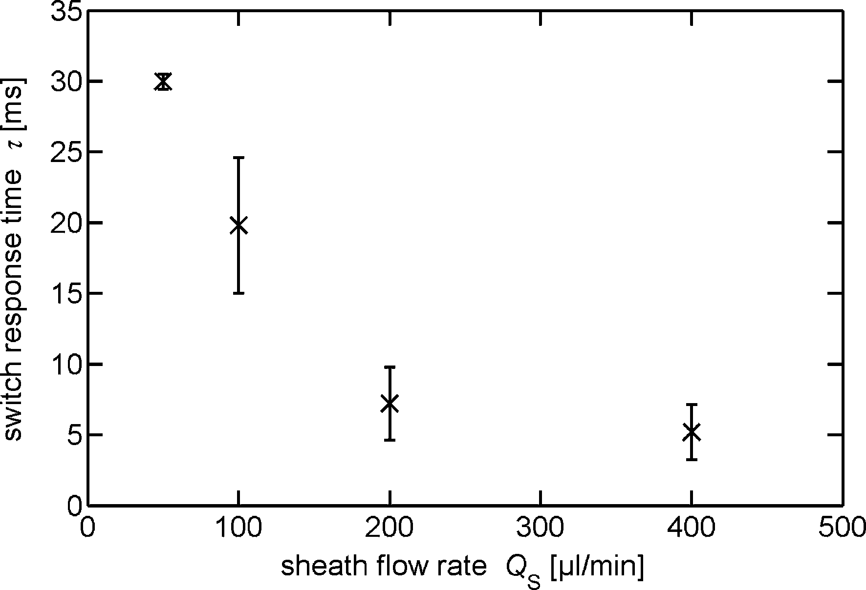 | ||
| Fig. 9 Switch response times τ at different sheath flow rates QS. Decreasing response times at increasing sheath flow rates are observed. Error bars indicate the standard deviation of repetitive experiments. | ||
For shorter switch response times a redesign of the fluidic network is necessary. An approach is to reduce the transit time of the heated sheath flow by shortening of the narrow sections, to reduce the cross sections and to reduce the inertial mass of the sheath flow, by decreasing the length and diameter of the upstream sheath flow channels.
Fig. 10(A) shows the displacement DA at different absorbed radiant fluxes as a function of time for a sheath flow rate of 200 μl min−1. At absorbed radiant fluxes above 500 mW the analyte flow displacement, determined by the Gaussian fitting routine, decreases directly after the maximum peak, which is caused by an asymmetric widening of the analyte flow starting 15 ms after onset of the heating. The widening is probably a result of the formation of vortices at the conjunction.
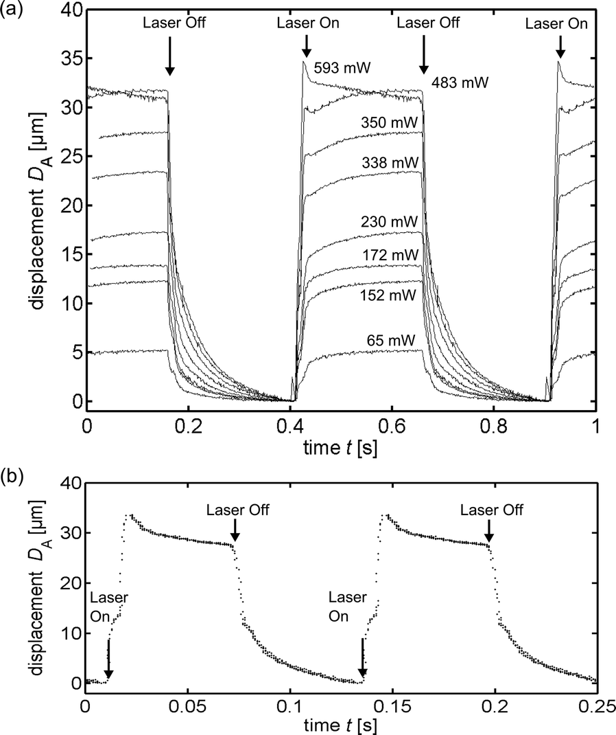 | ||
| Fig. 10 Displacement of the dyed analyte flow DA as a function of time. The displacement is determined by fitting a Gaussian curve to the grey levels of the images along a column, depicted in Fig. 5 as the vertical y-axis. The images are captured with a time-stamp and resorted to fit into one period of switching. The interval between two images is 4 to 5 ms. The data points are doubled and depicted consecutively to illustrate the periodicity. In (a) switching is executed at 2 Hz at different absorbed powers from 65 mW up to 593 mW and in (b) at 8 Hz and 736 mW. The sheath flows are (a) 200 μl min−1 and (b) 400 μl min−1 and the analyte flows are (a) 7 μl min−1 and (b) 5 μl min−1. | ||
Maximum switchable analyte flow
With increasing sheath flow rates larger flow rates of analyte can be switched and more radiant flux for heating can be used, prior to the formation of boiling bubbles, see Fig. 11. The maximum switchable analyte flow rates for up to 1 W of absorbed radiant flux or up to the formation of boiling bubbles are 0.2 μl min−1, 1.5 μl min−1, 3.8 μl min−1 and 6.1 μl min−1 at the sheath flow rates of 50 μl min−1, 100 μl min−1, 200 μl min−1 and 400 μl min−1, respectively.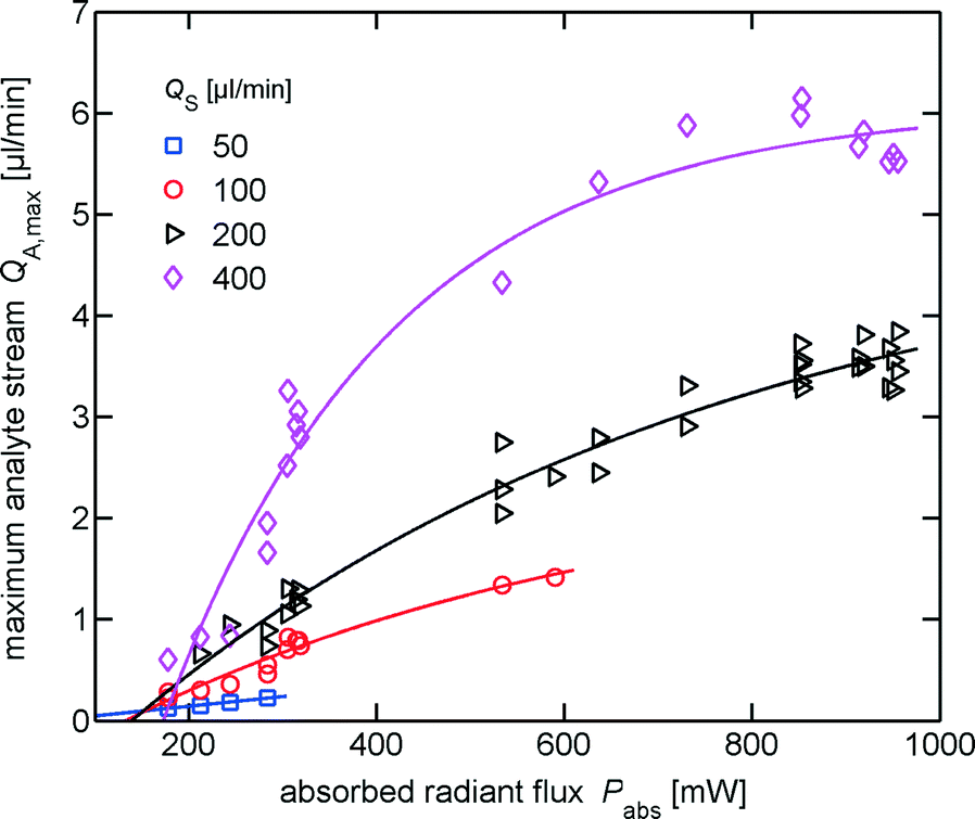 | ||
| Fig. 11 The maximum analyte flow varies with the amount of absorbed radiant flux and the sheath flow rate. The data points for Q_S= 50 μl min−1 and 100 μl min−1 are limited because of the generation of bubbles due to boiling at higher absorbed powers. The solid lines are fitted using an exponential function as a guide for the eye. | ||
Switching particles
For the 200 μl min−1 sheath flow, 5 μl min−1 analyte flow and an absorbed optical power of ∼740 mW we investigated switching frequencies of 4 Hz and 8 Hz. Although the theoretical value of QA,max is approximately 3 μl min−1, in the experiment larger values are observed. We observed (91 ± 5)% true-positive and (81 ± 9)% true-negative particles for 4 Hz. At 8 Hz switching frequency we determined (84 ± 10)% true-positive and (96 ± 8)% true-negative particles. Within the errors these values are identical. A reduction of the undesirable false-positive and false-negative is expected for larger QA,max. This can be done by increasing the sheath flow rate, which also increases the fluid consumption and the analyte dilution, or a redesign of the microfluidic network by increasing the hydrodynamic resistance at the narrow sections.The integration of a fluorescence sensor and triggered switching is planned in the near future, which will enable shorter switching periods with higher radiant fluxes without risk of formation of boiling bubbles. Hence with triggered switching better sorting performance is expected.
Conclusions
Using the possibility to fabricate complex three-dimensional microfluidic systems by SLE, we demonstrated an optically driven switch for particle sorting. Due to the excellent optical properties of fused silica the integration of highly sensitive fluorescence sensors is possible, enabling the realisation of an all-optical μFACS system with a monolithic chip. High-speed video recordings indicate the possibility of realising sorting frequencies of up to 200 Hz at a high analyte flow rate of 10 μl min−1.‡Acknowledgements
This work was supported by the German Federal Ministry of Education and Research (BMBF, 16SV5443K) and the Fraunhofer-Gesellschaft zur Förderung der angewandten Forschung e.V.Notes and references
- C. W. Shields, C. D. Reyes and G. P. López, Lab Chip, 2015, 15(5), 1230 RSC.
- R. Applegate, J. Squier, T. Vestad, J. Oakey and D. Marr, Opt. Express, 2004, 12(19), 4390 CrossRef PubMed.
- F. Bragheri, P. Minzioni, R. Martinez Vazquez, N. Bellini, P. Paiè, C. Mondello, R. Ramponi, I. Cristiani and R. Osellame, Lab Chip, 2012, 12(19), 3779 RSC.
- J. Enger, M. Goksör, K. Ramser, P. Hagberg and D. Hanstorp, Lab Chip, 2004, 4(3), 196 RSC.
- M. M. Wang, E. Tu, D. E. Raymond, J. M. Yang, H. Zhang, N. Hagen, B. Dees, E. M. Mercer, A. H. Forster, I. Kariv, P. J. Marchand and W. F. Butler, Nat. Biotechnol., 2004, 23(1), 83 CrossRef PubMed.
- X. Wang, S. Chen, M. Kong, Z. Wang, K. D. Costa, R. A. Li and D. Sun, Lab Chip, 2011, 11(21), 3656 RSC.
- M. P. MacDonald, G. C. Spalding and K. Dholakia, Nature, 2003, 426(6965), 421 CrossRef CAS PubMed.
- T. D. Perroud, J. N. Kaiser, J. C. Sy, T. W. Lane, C. S. Branda, A. K. Singh and K. D. Patel, Anal. Chem., 2008, 80(16), 6365 CrossRef CAS PubMed.
- M. de Robert Saint Vincent, R. Wunenburger and J.-P. Delville, Appl. Phys. Lett., 2008, 92(15), 154105 CrossRef.
- Y. Chen, A. J. Chung, T.-H. Wu, M. A. Teitell, D. Di Carlo and P.-Y. Chiou, Small, 2014, 10(9), 1746 CrossRef CAS PubMed.
- T.-H. Wu, Y. Chen, S.-Y. Park, J. Hong, T. Teslaa, J. F. Zhong, D. Di Carlo, M. A. Teitell and P.-Y. Chiou, Lab Chip, 2012, 12(7), 1378 RSC.
- K. Ozaki, H. Sugino, Y. Shirasaki, T. Aoki, T. Arakawa, T. Funatsu and S. Shoji, Sens. Actuators, B, 2010, 150(1), 449 CrossRef CAS.
- M. Haneoka, Y. Shirasaki, H. Sugino, T. Aoki, T. Arakawa, K. Ozaki, D. H. Yoon, N. Ishii, R. Iizuka, S. Shoji and T. Funatsu, Sens. Actuators, B, 2011, 159(1), 314 CrossRef CAS.
- L.-M. Fu, R.-J. Yang, C.-H. Lin, Y.-J. Pan and G.-B. Lee, Anal. Chim. Acta, 2004, 507(1), 163 CrossRef CAS.
- H. J. Kim, H.-S. Moon, B. S. Kwak and H.-I. Jung, Sens. Actuators, B, 2011, 160(1), 1536 CrossRef CAS.
- A. J. de Mello and J. B. Edel, J. Appl. Phys., 2007, 101(8), 084903 CrossRef.
- N. Pamme, R. Koyama and A. Manz, Lab Chip, 2003, 3(3), 187 RSC.
- T. D. Perroud, J. N. Kaiser, J. C. Sy, T. W. Lane, C. S. Branda, A. K. Singh and K. D. Patel, Anal. Chem., 2008, 80(16), 6365 CrossRef CAS PubMed.
- T. Schulz, S. Poser, E. Ermantraut, J. McCaskill, H. P. Mathis and J. M. Köhler, in Proceedings of the uTAS '98 Workshop, held in Banff, Canada, 13–16 October 1998, Micro Total Analysis Systems '98, ed. D. J. Harrison and A. Berg, Springer Netherlands, Dordrecht, 1998, p. 303 Search PubMed.
- Y.-C. Tung, M. Zhang, C.-T. Lin, K. Kurabayashi and S. J. Skerlos, Sens. Actuators, B, 2004, 98(2–3), 356 CrossRef CAS.
- M. M. Wang, E. Tu, D. E. Raymond, J. M. Yang, H. Zhang, N. Hagen, B. Dees, E. M. Mercer, A. H. Forster, I. Kariv, P. J. Marchand and W. F. Butler, Nat. Biotechnol., 2004, 23(1), 83 CrossRef PubMed.
- B. Yao, G.-a. Luo, X. Feng, W. Wang, L.-x. Chen and Y.-m. Wang, Lab Chip, 2004, 4(6), 603 RSC.
- M. A. Unger, H.-P. Chou, T. Thorsen, A. Scherer and S. R. Quake, Science, 2000, 288(5463), 113 CrossRef CAS PubMed.
- R. Miyake, H. Ohki, I. Yamazaki and T. Takagi, JSME Int. J., Ser. B, 1997, 40(1), 106 CrossRef.
- D. Sobek, A. M. Young, M. L. Gray and S. D. Senturia in Proceedings An Investigation of Micro Structures, Sensors, Actuators, Machines and Systems, ed. D. Sobek, A. M. Young, M. L. Gray and S. D. Senturia, IEEE, 1993, p. 219 Search PubMed.
- A. Wolff, I. R. Perch-Nielsen, U. D. Larsen, P. Friis, G. Goranovic, C. R. Poulsen, J. P. Kutter and P. Telleman, Lab Chip, 2003, 3(1), 22 RSC.
- Y. Chen, A. J. Chung, T.-H. Wu, M. A. Teitell, D. Di Carlo and P.-Y. Chiou, Small, 2014, 10(9), 1746 CrossRef CAS PubMed.
- C. Simonnet and A. Groisman, Anal. Chem., 2006, 78(16), 5653 CrossRef CAS PubMed.
- J. P. Golden, J. S. Kim, J. S. Erickson, L. R. Hilliard, P. B. Howell, G. P. Anderson, M. Nasir and F. S. Ligler, Lab Chip, 2009, 9(13), 1942 RSC.
- X. Mao, J. R. Waldeisen and T. J. Huang, Lab Chip, 2007, 7(10), 1260 RSC.
- S. Chung, S. J. Park, J. K. Kim, C. Chung, D. C. Han and J. K. Chang, Microsyst. Technol., 2003, 9(8), 525 CrossRef CAS.
- P. Paiè, F. Bragheri, R. M. Vazquez and R. Osellame, Lab Chip, 2014, 14(11), 1826 RSC.
- A. Vogel, J. Noack, G. Hüttman and G. Paltauf, Appl. Phys. B: Lasers Opt., 2005, 81(8), 1015 CrossRef CAS.
- P. Abgrall, C. Lattes, V. Conédéra, X. Dollat, S. Colin and A. M. Gué, J. Micromech. Microeng., 2006, 16(1), 113 CrossRef.
- J. M. Yang, J. Bell, Y. Huang, M. Tirado, D. Thomas, A. H. Forster, R. W. Haigis, P. D. Swanson, R. Wallace, B. Martinsons and M. Krihak, Biosens. Bioelectron., 2002, 17(6–7), 605 CrossRef CAS PubMed.
- P. Abgrall and A.-M. Gué, J. Micromech. Microeng., 2007, 17(5), R15 CrossRef.
- D. Bhusari, H. A. Reed, M. Wedlake, A. M. Padovani, S. Allen and P. A. Kohl, J. Microelectromech. Syst., 2001, 10(3), 400 CrossRef CAS.
- Y. Liao, J. Song, E. Li, Y. Luo, Y. Shen, D. Chen, Y. Cheng, Z. Xu, K. Sugioka and K. Midorikawa, Lab Chip, 2012, 12(4), 746 RSC.
- Y. Mizukami, D. Rajniak, A. Rajniak and M. Nishimura, Sens. Actuators, B, 2002, 81(2–3), 202 CrossRef CAS.
- C. I. Rogers, K. Qaderi, A. T. Woolley and G. P. Nordin, Biomicrofluidics, 2015, 9(1), 016501 CrossRef PubMed.
- M. Hermans, J. Gottmann and A. Schiffer in SPIE Proc Ser, ed. F. G. Bachmann, W. Pfleging, K. Washio, J. Amako, W. Hoving and Y. Lu, SPIE, 2012, p. 82440E Search PubMed.
- M. Hermans, J. Gottmann and F. Riedel, J. Laser Micro/Nanoeng., 2014, 9(2), 126 CrossRef.
- L. Kou, D. Labrie and P. Chylek, Appl. Opt., 1993, 32(19), 3531 CrossRef CAS PubMed.
Footnotes |
| † Electronic supplementary information (ESI) available. See DOI: 10.1039/c5lc01478f |
| ‡ Supporting stroboscopic video recordings at switching frequencies of 200 Hz are available online. |
| This journal is © The Royal Society of Chemistry 2016 |