
 Open Access Article
 This Open Access Article is licensed under a Creative Commons Attribution-Non Commercial 3.0 Unported Licence
Recent developments in nanowires for bio-applications from molecular to cellular levels
Sakon
Rahong
*ab,
Takao
Yasui
*abc,
Noritada
Kaji
abd and
Yoshinobu
Baba
*abe
aDepartment of Applied Chemistry, Graduate School of Engineering, Nagoya University, Furo-cho, Chikusa-ku, Nagoya 464-8603, Japan. E-mail: sakon.rahong@apchem.nagoya-u; yasui@apchem.nagoya-u.ac.jp; babaymtt@apchem.nagoya-u.ac.jp; Fax: +81 52 789 3560; Tel: +81 52 789 3560; Tel: +81-52-789-4666; Tel: +81 -52 -789 -4611; Fax: +81-52-789-4666; Tel: +81-52-789-4664
bImPACT Research Center for Advanced Nanobiodevices, Nagoya University, Japan
cJST, PRESTO, Graduate School of Engineering, Nagoya University, Japan
dERATO Higashiyama Live-Holonics Project, Graduate School of Science, Nagoya University, Japan
eHealth Research Institute, National Institute of Advanced Industrial Science and Technology (AIST), Takamatsu 761-0395, Japan
First published on 17th February 2016
Abstract
This review highlights the most promising applications of nanowires for bioanalytical chemistry and medical diagnostics. The materials discussed here are metal oxide and Si semiconductors, which are integrated with various microfluidic systems. Nanowire structures offer desirable advantages such as a very small diameter size with a high aspect ratio and a high surface-to-volume ratio without grain boundaries; consequently, nanowires are promising tools to study biological systems. This review starts with the integration of nanowire structures into microfluidic systems, followed by the discussion of the advantages of nanowire structures in the separation, manipulation and purification of biomolecules (DNA, RNA and proteins). Next, some representative nanowire devices are introduced for biosensors from molecular to cellular levels based on electrical and optical approaches. Finally, we conclude the review by highlighting some bio-applications for nanowires and presenting the next challenges that must be overcome to improve the capabilities of nanowire structures for biological and medical systems.
1. Introduction
Over the past ten years, nanotechnology has emerged as one of the newest essential technologies, with applications in a wide range of fields, such as physics, chemistry, and biology. Nanotechnology produces an enormous number of nanostructures with different unique structural and functional features for various applications. Among the nanostructures, nanowires have a one-dimensional nanostructure, with a diameter on the order of 10−9 m, and they can be synthesized by different methods.1–15 Nanowires have been synthesized through bottom-up self-assembly processes such as metal catalyst-assisted laser ablation synthesis,4 solution phase synthesis5–7 and template-based methods.8,9 Other ways to prepare nanowire structures by top-down approaches have been demonstrated such as metal-assisted chemical etching10–12 and electron beam lithography.13–15 Two features of nanowires are that they can be highly sensitive sensors due to their large surface-to-volume ratio,16–18 and they can be short response-time sensors due to their well-defined geometry.19,20 To date, numerous applications of nanowires have been reported in semiconductor electronics,21–25 biochemistry,26–30 environmental science31–33 and medical diagnostics.34–37In this review, we focus on the recent applications of nanowires in analytical biochemistry applications, especially separation, filtration, and manipulation of biomolecules which are possible due to the diameter dimension of the nanowires being similar to the size of biomolecules, including DNA, RNA, and proteins. And, we also focus on the sensing ability of nanowires to cells because the diameter dimension of the nanowires is small enough to have a stealth effect against cells. Therefore, we discuss bio-applications of nanowires on the order of molecular to cellular levels (10−10–10−6 m). In brief, this review is organized as follows: discussion of the integration between nanowires and microfluidic systems for biomolecule analysis such as mechanical cell lysis, DNA manipulation, biomolecule separation and filtration; description of nanowires for a specific medical diagnostic use such as capturing circular tumor cells (CTCs); and descriptions of biosensors based on nanowires, nanowire structure interfaces with cells, and nanowires for synthesized tissues, including some future challenges for nanowire structures.
2. Bio-applications: biomolecule analysis
2.1 Mechanical cell lysis
Cell lysis is an initial and critical process in analysis of intracellular components. Several approaches have been established and developed such as chemical, electrical and mechanical methods. However, chemical cell lysis requires many steps and consumes many reagents to purify the biomolecule samples and the potential for occurrence of harmful effects on microorganisms is high.38,39 Electrical cell lysis is less harmful than chemical cell lysis but it is still expensive and has a low throughput.40,41 As mentioned above, the diametric size of the nanowires is smaller than that of cells, and therefore the nanowire tip can penetrate and disrupt the cellular membrane function.42 This has allowed researchers to extract microorganisms in cells faster than in previous methods. As a demonstration of mechanical cell lysis using nanowires, Kim et al.43 prepared ZnO nanowires (diameter: −100 nm) on the surface of a pillar array in a microchannel by a low temperature hydrothermal reaction method. They combined the nanowires with a microfluidic system for mechanical cell lysis when HaCaT cells were flowing around the nanowires in the poly(dimethylsiloxane) (PDMS) microchannel, and the combined device also allows observation of the deformation of HaCaT cells. This method has a higher extraction efficiency for nucleic acids and proteins than using chemical cell lysis methods.For easy and rapid mechanical cell lysis, So et al.44 fabricated a porous Si membrane (average pore diameter, 75 nm) by utilizing a photolithography process and photoelectrochemical etching, then ZnO nanowires (ZnO NWs) were synthesized on the Si membrane by a low temperature hydrothermal reaction method (Fig. 1). After that, SiO2 was grown on the backside of the membrane by plasma-enhanced chemical vapor deposition to form a selective adsorption layer of DNA molecules. The nanowire membrane was attached with a commercial handheld syringe filter holder as illustrated in Fig. 1. After the HepG2 cells were injected by the syringe and approached the nanowires, the tips of the nanowires penetrated into the cells, and then the biomolecules spilled out and passed through the Si membrane, while the cell membrane is still in contact with the nanowire structures. Only the DNA molecules were adsorbed at the SiO2 layer by the formation of hydrogen bonds and intermolecular electrostatic force. Lastly, a buffer solution was injected to wash out any debris and remaining proteins before collecting the isolated DNA molecules. The total processing time for mechanical cell lysis by the nanowire membrane took only 5 min with higher extraction efficiency for proteins and nucleic acids than that obtained for commercially available kits. Future work should focus on the purification of biomolecules such as DNA, RNA and proteins after extraction of cells.
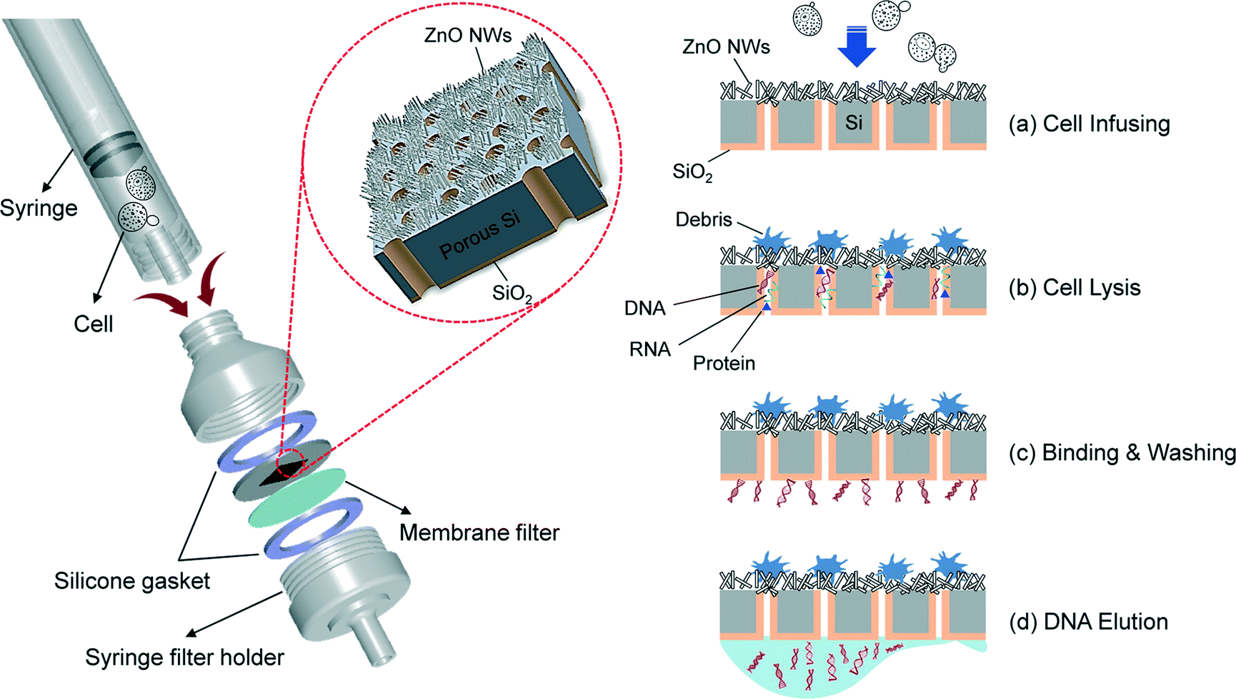 | ||
| Fig. 1 Schematic of the direct assembly of the nanowire-decorated multifunctional membrane with a commercial handheld syringe filter holder for mechanical cell lysis and DNA purification. The overall sequential process is shown in (a)−(d). Reprinted with permission.44 Copyright 2014 American Chemical Society. | ||
2.2 Biomolecule separation and filtration
Biomolecule separation and analysis are essential processes for analytical and biological development. Conventional gel electrophoresis has a limitation for separation of long DNA molecules and it requires several hours to analyze biomolecules. Integrations between nanostructures by top-down approaches and microfluidic systems, such as nanopillar array structures,45–47 nanowalls,48 and nanofence structures,49 have been proposed to overcome the problems, however, difficulty in fabricating them using an electron beam lithography process with the high investment in a sophisticated system has slowed down their development. On the other hand, self-assembly bottom-up approaches, such as magnetic colloidal nanoparticles50–52 and core–shell nanoballs,53 offer ease of fabrication and separations of biomolecules have been reported for them; however, low reusability of the materials for these approaches still has a size limitation, hampering their development. To overcome the bottom-up related issue, self-assembled nanowire structures of metal oxides have been used as sieving materials and their rigidity offers high reusability.We have integrated SnO2 nanowires into fused silica microchannels by using the photolithography process and vapor liquid solid technique (VLS) as shown in Fig. 2a.54 The special feature of the nanowire structure is the controllability of pore size (20–400 nm) by varying the number of nanowire growth times as a cycle; consequently, we obtained a hyper-branched nanowire network structure as illustrated in Fig. 2b–e. Then we measured and calculated the dependence of the electrophoretic mobility of DNA molecules in the nanowire networks as shown in Fig. 2f. Based on the mobility difference, we could separate λ DNA digested by the Hind III enzyme within 13 s under an applied DC electric field of 500 V cm−1 as illustrated in Fig. 2g. In addition, the hyper-branched nanowire structure has also been employed as a sieving material to separate small DNA molecules (0.05–1 kbp), proteins (20–340 kDa) and RNA ladders (0.1–1 kb) as shown in Fig. 3.55 Moreover, we demonstrated that highly dense nanowires, serving as a molecular filter, could provide high throughput filtration of DNA molecules from a mixture of λ DNA and T4 DNA within 1 s.56 The surprising biomolecule separations and filtrations described above highlight the outstanding properties of the nanowire structures integrated with the microfluidic channel. These findings are promising, and in future, they should lead to separation and analysis of other biomolecules.
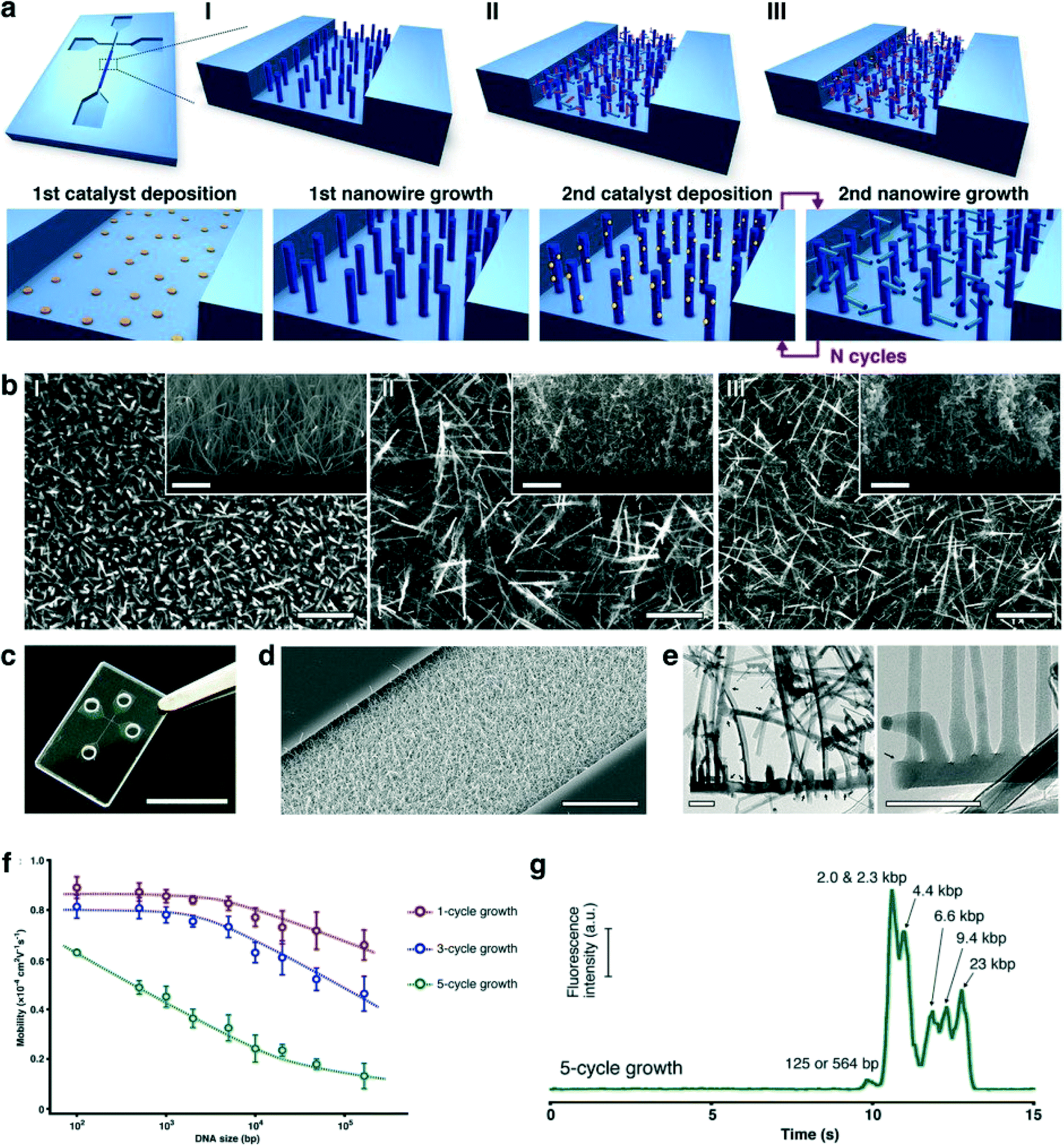 | ||
| Fig. 2 3D nanowire network structure. (a) Schematic illustrations showing the nanowire structure after: (I) 1-cycle growth; (II) 3-cycle growth, and (III) 5- cycle growth; and (lower row) the overall fabrication procedure. The microchannel and nanowire network structure are formed on a fused silica substrate. (b) SEM images (scale bar, 1 μm) of the nanowire network structure showing: (I) 1-cycle growth; (II) 3-cycle growth; and (III) 5-cycle growth. The insets show vertical cross-sectional SEM images; scale bar, 1 μm. (c) Photograph of the fabricated device; scale bar, 1 cm. (d) SEM image of the nanowire network structure embedded in the microchannel; scale bar, 10 μm. (e) TEM images of the nanowire network structure; scale bars, 100 nm (left) and 50 nm (right). Black arrows highlight branched positions. (f) Dependence of electrophoretic mobility on DNA size in the nanowire network structure with 1-cycle growth nanowires (red circles), 3-cycle growth nanowires (blue circles), and 5-cycle growth nanowires (green circles). Error bars show the standard deviation for a series of measurements (N = 3). (g) Separation of lambda DNA digested by Hind III in the nanowire network structure with 5-cycle growth nanowires. The electropherogram was obtained at 3 mm from the entrance of the microchannel with the nanowire network structure. The applied DC electric field in the separation channel was 500 V cm−1. Modified and reprinted with permission.54 Copyright 2014 Nature Publishing Group. | ||
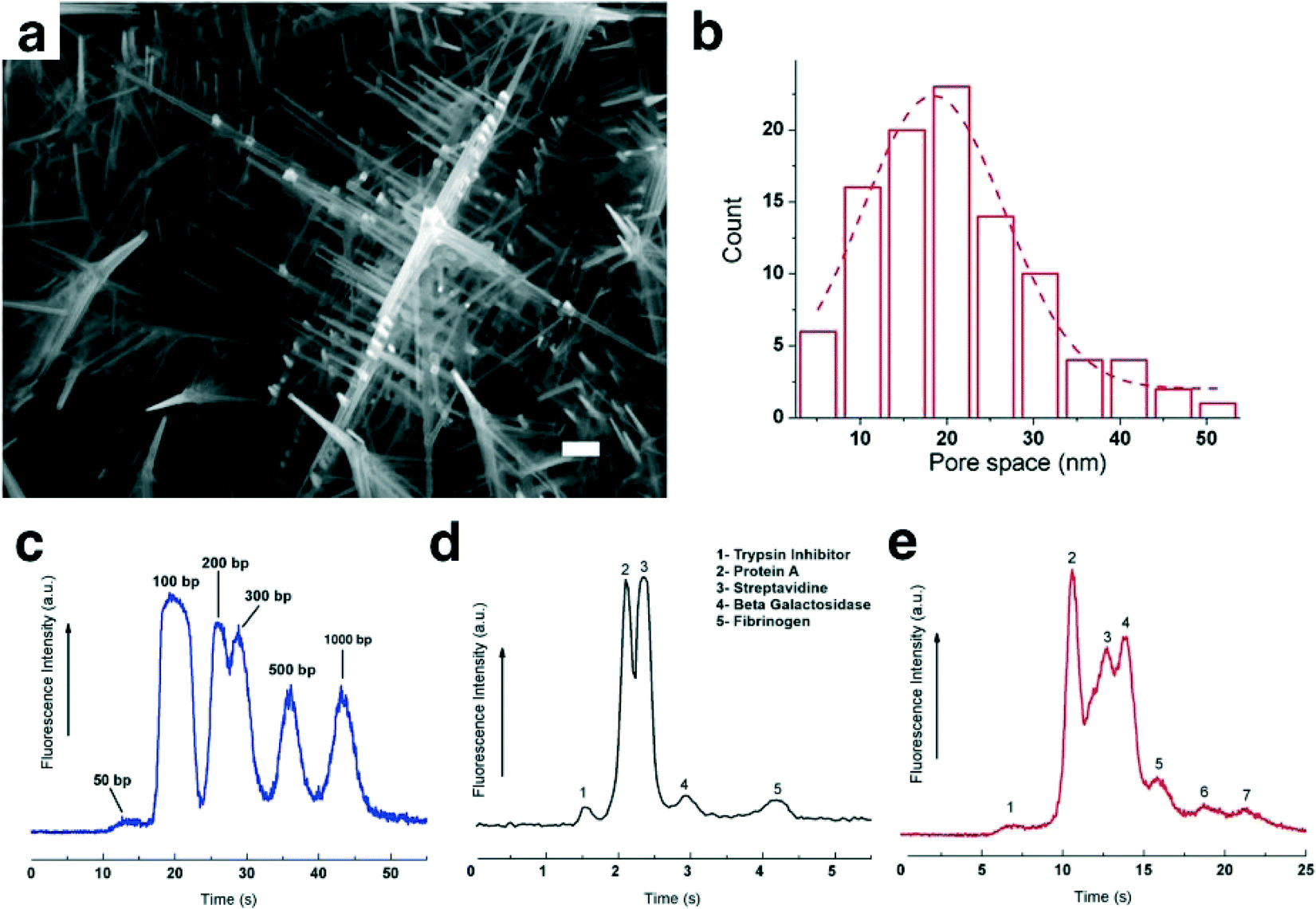 | ||
| Fig. 3 (a) SEM image of the 3D nanowire structures; scale bar 100 nm. (b) Pore size distribution in the 3D nanowire structures. (c) Separation of 50 bp (40 ng μL−1), 100 bp (30 ng μL−1), 200 bp (30 ng μL−1), 300 bp (30 ng μL−1), 500 bp (30 ng μL−1) and 1000 bp (30 ng μL−1) molecules in the 3D nanowire structures. The electropherograms were obtained at 500 μm from the entrance of the 3D nanowire structures. The applied electric field in the separation channel was 100 V cm−1. (d) Separation of (1) trypsin inhibitor (20.1 kDa), (2) protein A (45 kDa), (3) streptavidin (52.8 kDa), (4) β-galactosidase (116 kDa) and (5) fibrinogen (340 kDa). The electropherograms were obtained at 2000 μm from the entrance of the 3D nanowire structures. The applied electric field in the separation channel was 500 V cm−1. (e) Separation of 0.1–1 kb RNA molecules in the 3D nanowire structures. The electropherogram was obtained at 250 μm from the entrance of the 3D nanowire structures. The applied electric field in the separation channel was 300 V cm−1. Modified and reprinted with permission.55 Copyright 2015 Nature Publishing Group. | ||
2.3 DNA manipulation
A number of research studies in recent years have focused on the next next-generation genome sequencer using nanopore structures. In the next next-generation genome sequencer, tunneling or ionic-blocking currents for each nucleotide were measured when DNA molecules translocated into nanopore devices;57–61 however, elongation and manipulation of long DNA molecules before translocation into nanopore devices is still a challenging issue.62–65 Researchers have reported calculation models or manipulation experiments for long DNA molecules, such as the rope-over-pulley model and biased reptation.66,67 Bustamante et al.68 proposed that the radius of a thinned post should correspond with the Kuhn length of DNA (lk ≈ 106 nm). We verified this proposal by an experiment in which spot arrayed SnO2 nanowires in fuse silica microchannels elongated T4 DNA (166 kbp) molecules under an applied DC electric field.69Fig. 4a and b show that the T4 DNA molecules could be elongated to more than 80% of their fully elongated length. We found that the “M”-shaped conformation, which is uniquely seen for DNA migration only in spot arrayed nanowires, plays an important role in manipulating long DNA molecules as illustrated in Fig. 4c–f. Recently, next generation nanopore DNA sequencing devices still have limitation in terms of reading the length and it is still difficult for them to control the translocation speed. These finding points are promising to improve the efficiency of nanopore DNA sequencing devices for single strand DNA elongation and controlling the DNA translocation velocity through nanopore devices.61,68 However, preparation methods of nanowire structures still need to be developed and the diameter of nanowire structures needs to be reduced to elongate single strand DNA molecules, which have a Kuhn length of approximately 10 nm.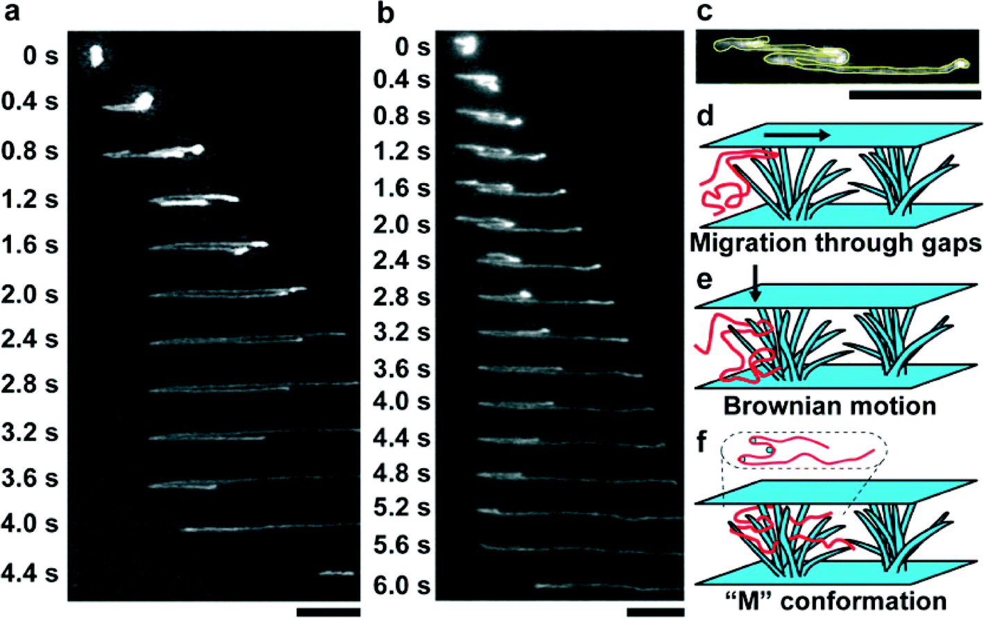 | ||
| Fig. 4 (a) Time-course observations of a T4-DNA molecule in spot arrayed nanowires under an applied electric field of 10 V cm−1; scale bar, 10 μm. (b) Time-course observations of a T4-DNA molecule in the spot arrayed nanowires under an applied electric field of 10 V cm−1; scale bar, 10 μm. The T4-DNA molecule shows the characteristic “M”-shaped conformation from 0.8 to 2.0 s. (c) “M”-shaped conformation in the spot arrayed nanowires; scale bar, 10 μm. The outline of the DNA molecule is highlighted as the yellow line. The image is the magnified image at 1.6 s in (b). (d–f) Schematic illustrations showing the formation of the “M”-shaped conformation in the nanowire spot array structure: (d) a DNA molecule migrates through gaps between the nanowires and the cover plate; (e) the migrating DNA molecule settles into the nanowire array structure by Brownian motion; (f) the DNA molecule, now with the “M”-shaped conformation (presented as a top view inside the dotted oval), is entangled with the nanowire array structure. Reprinted with permission.69 Copyright 2013 American Chemical Society. | ||
2.4 Nanowires for detection of circulating tumor cells (CTCs)
CTCs play an important role in cancer metastasis, and their presence in blood samples of cancer patients provides information about the type of cancer. For example, Hosokawa et al.70 proposed an array of microcavities to perform size-selective capture of CTCs. Soper' group demonstrated the preconcentration of CTCs from blood cells by electrokinetic enrichment devices with CTC selection efficiency more than 90%.71 And, Toner's group reported a herringbone chip (HB chip) to capture and isolate clusters of CTCs from the blood of patients, which has a capture efficiency of more than 80%.72 However, these techniques could not control the release of CTCs for further analysis. To overcome the above issue, Tseng and his research team developed Si nanowires, which they called a NanoVelcro chip, to capture and release CTCs from blood samples with high selectivity.73–76 Si nanowires were fabricated on substrates by a standard photolithography and chemical wet etching process, and then they were bonded on chaotic mixer microfluidic channels to fabricate the NanoVelcro chip. Surface modification with cell surface markers of anti-EpCAM enhanced the capturing efficiency of CTCs or of anti-CD45 depleted white blood cells on the nanowires. Whole-blood samples collected from cancer patients were injected into the device as shown in Fig. 5. The NanoVelcro chip could capture CTCs on the surface with an efficiency of 40–70%. The NanoVelcro chip based on Si nanowires has been developed for single-CTC isolation by depositing thermoresponsive polymer brushes, poly(N-isopropylacrylamide (PIPAAm), on Si nanowires.74 This thermoresponsive NanoVelcro chip could capture and release CTCs at 37 °C and 4 °C, respectively. In addition, in the same study, biotin groups were introduced for conjugation of polymer brushes and anti-EpCAM to enhance the specific capture of CTCs. The efficiency of CTC release was nearly 90%. NanoVelcro chips are promising tools to capture and purify CTCs rapidly before CTC molecular analysis.73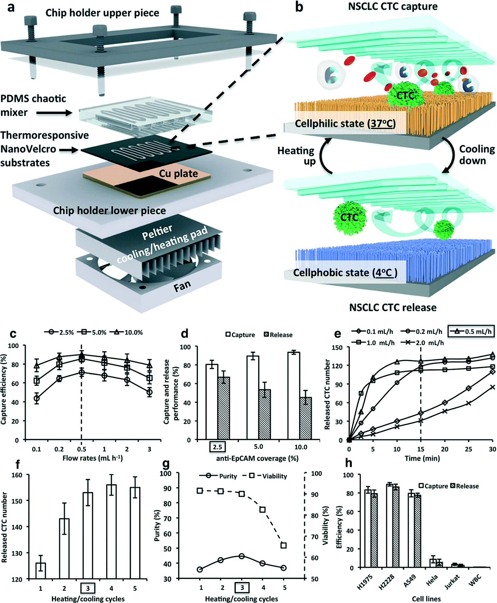 | ||
| Fig. 5 (a) Thermoresponsive NanoVelcro system for purification of CTCs (labeled in the drawings as NSCLC CTC). (a) A chip holder is employed to assemble a lithographically patterned thermoresponsive NanoVelcro substrate with an overlaid PDMS chaotic mixer. A Peltier cooling/heating pad (integrated with a thermocouple sensor) is located underneath the lower piece of the chip holder, enabling instant and precise temperature control of the system. (b) At 37 °C, the thermoresponsive NanoVelcro substrate is programmed to its “cellphilic” state. The chaotic mixer is capable of enhancing the contact frequency between the flowing-through CTCs and the substrate, leading to an improved CTC-capture performance. The substrate can effectively release CTCs at its “cellphobic” state (4 °C). Multiple heating/cooling cycles can further increase the efficiency of CTC release. (c) At 37 °C, variable cell-capture efficiencies were observed for three anti-EpCAM surface coverages (2.5, 5, and 10%) at different flow rates. The 0.5 mL h−1 flow rate gave the best cell-capture performance. (d) Cell-capture and release performances were observed for different anti-EpCAM coverages at 37 and 4 °C, respectively. (e) At 2.5% of anti-EpCAM coverage, differential cell-release performances were observed for different flow rates at 4 °C. The 0.5 mL h−1 flow rate gave the best cell-release performance. (f) Under the optimal cell release conditions, improved performances were observed with increased heating/cooling cycles. At least three heating/cooling cycles were required to effectively release the substrate-immobilized cells. (g) Heating/cooling cycles affected the viability and purity of recovered cells. (h) Performance observed for capturing and releasing EpCAM-positive cell lines (i.e., H1975, H2228, and A549) and EpCAM-negative cells (i.e., HeLa, Jurkat, and WBCs). Modified and reprinted with permission.74 Copyright 2014 American Chemical Society. | ||
3. Bio-applications: biosensors
Nanowire biosensor devices are opening doors to new approaches for identifying and quantifying biomolecules through nanosensors and nanoprobes. Since nanowires have a high surface-to-volume ratio and well-defined geometry, they have high sensitivity and short response time. These features are suited for uses in biological systems or chemical detection systems, especially at extremely low concentrations. Nanowires for bio-applications can be categorized into two major methodologies: electrical detection and optical detection.77,783.1 Electrical biosensors based on nanowires
The field effect transistor (FET) is an essential electronic component, which allows researchers to detect electrical signals related to chemical or biological actions. Mao et al.79 proposed the detection of protein binding (immunoglobulin G/IgG and anti-immunoglobulin/anti-IgG) conjugated with Au nanoparticles by a thermal-reduced graphene oxide field effect transistor (TRGO FET), and the detection limit of TRGO FET was 0.2 ng mL−1. Sarkar et al.80 also reported the highly sensitive label-free MoS2 FET structures. In these experiments, they could detect the interaction between biotin and streptavidin molecules in 0.01× PBS buffer solutions by measuring the pH value change at very low concentrations (−100 fM). However, 2D nanostructure devices are still difficult to use as sensing probes for intracellular detection like nanowire structure devices. In addition, Chen et al.81 have compared the DNA detection capability of a GaN thin film (GaNTF) with that of a GaN nanowire (GaNNW) FET structure. According to their results, GaNNW has 3 orders of magnitude higher sensitivity than the GaNTF device with a wider detection range (10−19–10−6 M) due to the large surface area of nanowires. Consequently, nanowire structures are promising for highly sensitive biological sensors. Semiconductor nanowires have been widely used as chemical and biological sensors which offer highly sensitive detection and analysis in real time through detection of a reaction on the nanowire surfaces. Top-down approaches, such as photolithography and electron beam lithography processes, are optimized to fabricate nanowire FET structures. Cui et al.26 reported the first silicon nanowire FET (SiNW FET) as a nanosensor for pH sensing and they modified specific receptors on the surfaces of SiNW to allow biological sensing. In addition, the SiNW FET was developed as a sensor array device for multiple detections such as viruses, cancer markers and DNA, through the covalent bond formation of a specific receptor on the surface of the SiNW.82Recently, Xie et al.83 proposed a new detection mechanism of charge-based sensing of DNA using nanowires with the FET. A short channel p-type SiNW FET was fabricated onto a SiNx membrane and a nanopore was drilled from one side to the other, as shown in Fig. 6a, to detect the change in conductance, instead of tunneling current, during DNA translocation through the nanopore. In this experiment, the buffer concentrations at the trans (nanopore and SiNW FET) chamber and cis (back side) chamber were optimized to obtain the translocation signals. The difference in the ratio of buffer salt concentrations between the cis and trans chambers could enhance the translocation signals of long single strand DNA molecules. The proportion between the ionic current signal and the order of magnitude of the FET signal was constant. This concept is likely to allow researchers to integrate the SiNW FET with a nanopore for multiplexed DNA sequencing at a higher throughput.
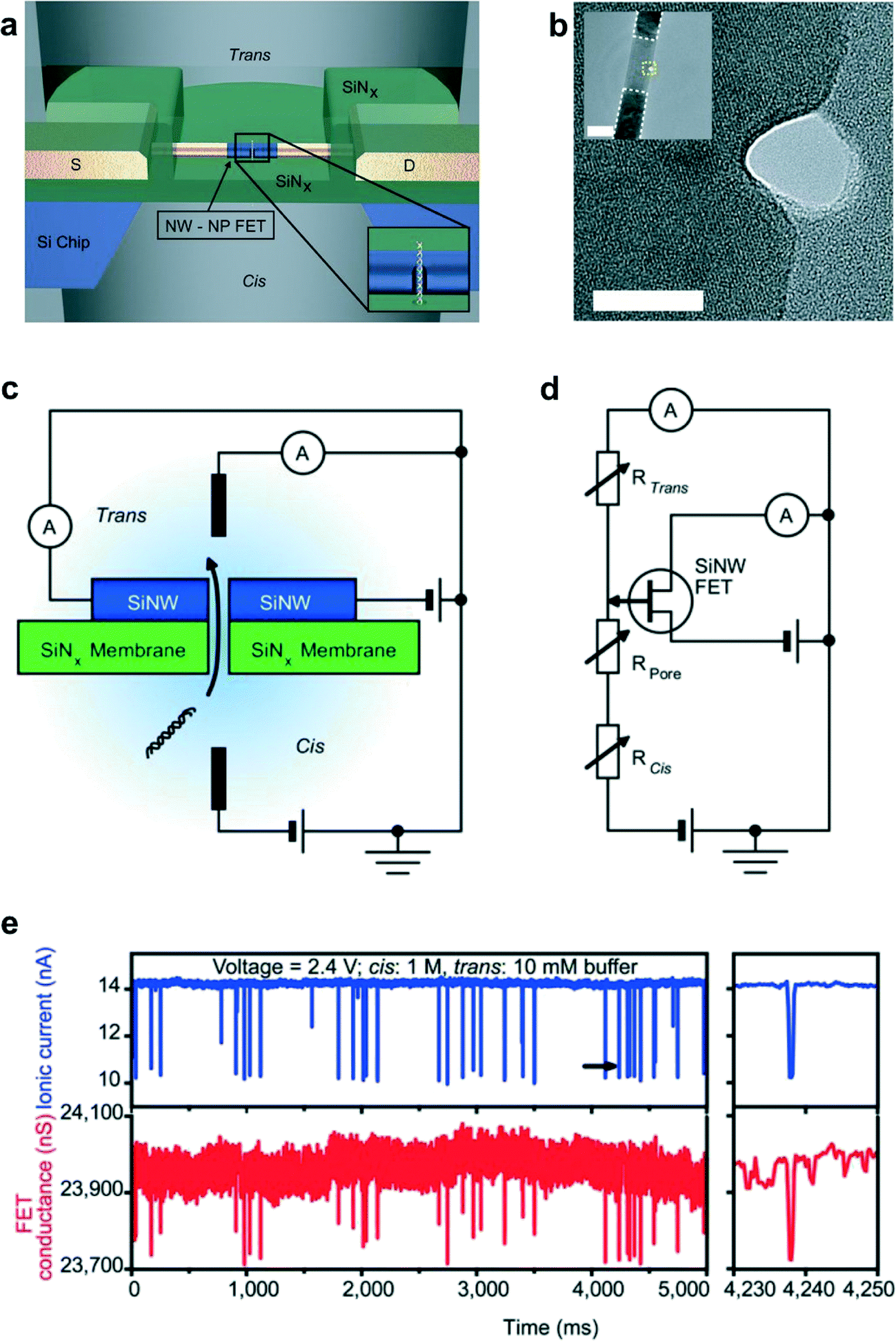 | ||
| Fig. 6 Nanowire–nanopore transistor. (a) Schematic of the nanowire–nanopore measurement set-up. Inset: zoom-in view around the nanopore. NW–NP, nanowire–nanopore. (b) High-resolution TEM image of a silicon nanowire with the nanopore off-axis at the nanowire edge. Scale bar, 10 nm. Inset: larger-scale TEM image of the nanowire–nanopore FET device showing the central silicon nanowire connected to darker NiSi contacts, which are indicated by the white dashed line. The region where the high-resolution TEM image was recorded is indicated by the yellow dashed square. Scale bar (inset), 50 nm. (c) Schematic of the sensing circuit. (d) Equivalent circuit diagram for (c). SiNW, silicon nanowire. (e) Simultaneously recorded ionic current and FET conductance FET signals with a trans chamber KCl buffer concentration of 10 mM, a cis chamber KCl buffer concentration of 1 M, and 1.4 nM pUC19 DNA. Right panels: zoom-in views of single ionic current and FET conductance events at the time indicated by black arrows in the ionic current traces of the corresponding left panels. Modified and reprinted with permission.83 Copyright 2012 Nature Publishing Group. | ||
Nanowire structures with the FET have been used as a probe to study microorganisms in living cells. Duan et al.84 introduced a branched intracellular nanotube FET (BIT-FET) to measure the potential in cardiomyocytes (heart cells). The nanowires were grown as branches on a p-SiNW FET structure, and then a SiO2 passivation layer was deposited on the nanowires. After that, chemical etching of the nanowires formed the silica nanotubes (diameter: 50–150 nm) on the SiNW FET as depicted in Fig. 7a. The phospholipid was modified on nanotubes to improve the interaction with the cell membrane and prevent leakage of the cytosol during recording of the signal. Fig. 7b shows that the BIT FET could detect and measure the beating of cardiomyocytes. In another study, Robinson et al.85 reported a vertical electrode nanowire array (VNEA), which was used to stimulate and record extracellular electrical signals intracellularly in the nerve cells. Si nanowire arrays had metal deposited at the nanowire tips as illustrated in Fig. 7c and d. In Fig. 7e, the seal resistance between the VNEA and the cell membrane (0.1–0.5 GΩ) was about 10 times smaller than the seal resistance of the standard pipette and the cell membrane (2 GΩ); consequently the signal-to-ratio of the VNEA was higher than that of the standard pipette.
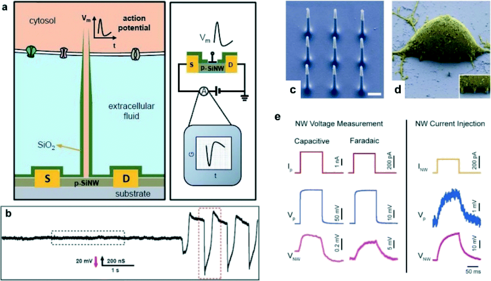 | ||
| Fig. 7 (a) Schematic diagrams showing (left) a cell coupled to a BIT-FET and the variation in device conductance G (right) with time t for an action potential Vm. S and D indicate the source and drain electrodes. The SiO2 nanotube connects the cytosol (orange) to the p-type silicon nanowire FET and, together with the SiO2 passivation layer (green), excludes the extracellular medium (light blue) from the active device channel. The structures on the membrane represent different ion channels, and are not scaled to the true size of the BIT-FET. (b) Representative trace (conductance versus time) reflecting the transition from extracellular to intracellular recording. Modified and reprinted with permission.84 Copyright 2012 Nature Publishing Group. (c) Scanning electron microscopy (SEM) image of the 9 silicon nanowires that constitute the active region of the VNEA fabricated by Robinson et al.85 Dimensions of the nanowire electrodes were designed to facilitate single-cell intracellular electrical coupling. False coloring shows metal-coated tips (gray) and insulating silicon oxide (blue). Scale bar, 1 μm. (d) SEM image of a rat cortical cell (3 days in vitro (DIV), false colored yellow) on top of a VNEA pad (false colored blue), showing nanowires interfaced with the cellular membrane (inset). (e) In both capacitive and Faradaic modes, the voltage response of the cell due to pipette current injection (Ip) (red) was recorded simultaneously using a patch pipette (Vp, blue) and a VNEA pad (VNW, magenta). Similarly, the cell membrane potential could be controlled (as verified by patch pipette recording) by injecting current through the nanowires (INW) (orange). Note that the capacitive and Faradaic measurements were performed on different cells since switching between recording modes required swapping amplifier electronics. Reprinted with permission.85 Copyright 2012 Nature Publishing Group. | ||
Recently, C. M. Lieber's group established a new paradigm shift and trend for bio-applications of nanowires as reported by Jiang et al.;86 they proposed a kinked nanowire structure, which was used as an active FET channel, for intracellular recording. A double-kinked tip was fabricated and wired to SU8 microelectrodes as a free-standing nanowire FET (nanoFET) probe inserted into a cell. The nanoFET probe could be bent by the stress release of the metal interconnection. The active area p–n junction of the nanoFET was modified by phospholipid treatment before use as the probe for cardiomyocytes that were cultured on the PDMS substrate. The results showed that the point-like nanoFET could record the extra- and intracellular signals simultaneously.87
Lieber's group also used the combination of nanowires and an FET integrated with biomaterials and synthetic tissues to fabricate a flexible and free-standing nanowire nanoelectronic scaffold (nanoES) as shown in Fig. 8a–d.88 In this work, they seamlessly merged nanowires and FET devices with metal interconnects as networks using artificial tissues of high porosity from the nanoscale to macroscale to produce three-dimensional nanoelectronic-tissue hybrids. The nanoES was used in experiments for formation of innervated tissues with cardiomyocytes, neurons and muscle cells. As one example, embryonic rat hippocampal neurons were cultured and merged with the nanoES and a conventional scaffold for 2 weeks. Fig. 8c and d show the 3D confocal images of the neurons as they passed through the ring-like structure of the nanowires and FET. Thus, the nanoES has a capability for long term monitoring during in vitro studies. In addition, the nanoES has been used to study drug effects by measuring intracellular signals from cardiomyocytes during injection of noradrenaline to stimulate cardiac contraction as illustrated in Fig. 8e–f. The next expectations of nanowires for biosensors are medical applications such as less invasive detection of nanoscale materials and implantable devices to stimulate and measure physiological quantities. These applications present some big research challenges for nanowires to overcome.
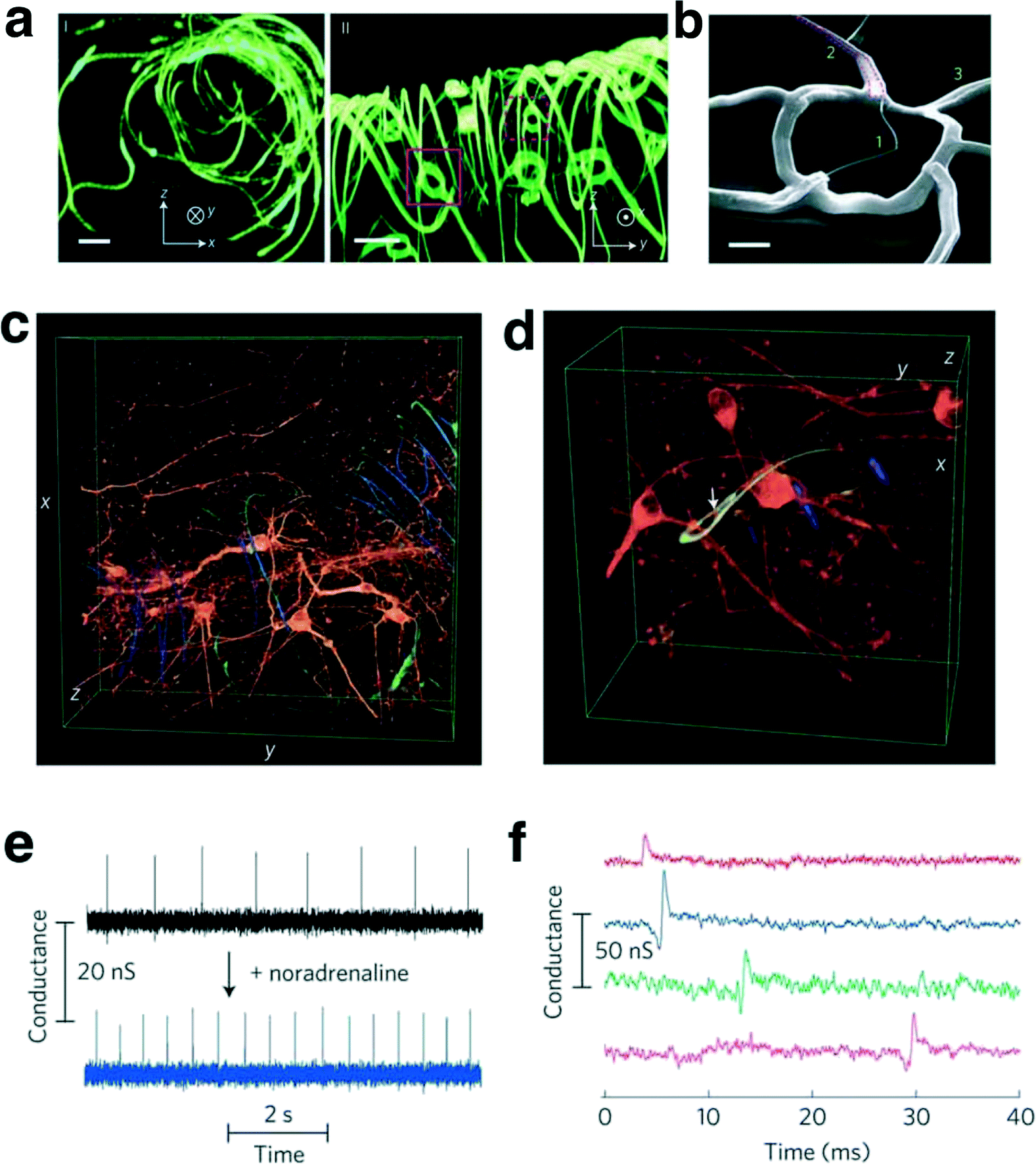 | ||
| Fig. 8 (a) 3D reconstructed confocal fluorescence micrographs of reticular nanoES viewed along the y (I) and x (II) axes. The scaffold was labelled with rhodamine 6G. The overall size of the structure, x – y – z = 300 – 400 – 200 μm. Solid and dashed open magenta squares indicate two nanowire FET devices located on different planes along the x axis. Scale bars, 20 μm. (b) SEM image of a single-kinked-nanowire FET within a reticular scaffold, showing (1) the kinked nanowire, (2) metallic interconnects (dashed magenta lines) and (3) the SU-8 backbone. Scale bar, 2 μm. (c, d) 3D reconstructed confocal images of rat hippocampal neurons after a two-week culture in Matrigel on reticular nanoES. Red (Alexa Fluor 546): neuronal β-tubulin; yellow (rhodamine 6G): epoxy ribbons. The metal interconnects are false-colored in blue, and are imaged in the reflected light mode. The white arrow highlights a neurite passing through a ring-like structure supporting a nanowire FET. Dimensions in (c), x: 317 μm; y: 317 μm; z: 100 μm; in (d), x: 127 μm; y: 127 μm; z: 68 μm. (e) Conductance versus time traces recorded from a single-nanowire FET before (black) and after (blue) applying noradrenaline. (f) Multiplex electrical recording of extracellular field potentials from four nanowire FETs in a mesh nanoES. Data are conductance versus time traces of a single spike recorded at each nanowire FET. Modified and reprinted with permission.88 Copyright 2012 Nature Publishing Group. | ||
3.2 Optical biosensors based on nanowires
Highly ordered one-dimensional structures of nanowires as arrays have been used for enhanced optical detection. For example, Huang et al.89 reported that an ordered Ag/SiNW array could detect the impact surface-enhanced Raman scattering (SERS) signal of various small molecules and salmon sperm dsDNA molecules. In this work, the finite-difference time-domain (FDTD) method was employed to simulate the near-field electric field distribution along the Ag surface on the SiNW array and the results were compared to the experimental values. The Ag/SiNW array detected SERS signals with a relative standard deviation of more than 14% for 4000 spots over a 200 × 200 μm2 array. The visualization of nanowires is essential for understanding the behaviors and mechanism of biological samples. Adolfsson et al.90 have demonstrated fluorescent semiconductor III–V heterostructure nanowires for biological and nanotoxicological studies. GaP–GaInP heterostructure nanowires were synthesized by a metal catalyst-assisted metal organic vapor phase epitaxy technique, and researchers could tune the emission wavelength from 925–560 nm. The nanowires were grown as barcode segments with different diameters and surface treatments. L929 fibroblasts were cultured on a substrate with nanowires and the fluorescence was observed using laser scanning confocal fluorescence microscopy. Individual nanowires were clearly observed as red dots which distinguished them from the living cells and tissues.Recently, P. D. Yang's group introduced nanowire-based single cell endoscopy to study molecular events with a high accuracy optical imaging system.91 A SnO2 nanowire was attached with a tapered single mode optical fiber and used as a waveguide to excite a transparent single living HeLa cell with a laser beam as shown in Fig. 9. The nanowire tip has high flexibility, and its small diameter with a high aspect ratio did not damage the cell, or rupture the membrane. Even though the cell was excited by the blue light through the nanowire tip, the light did not harm the cell due to the small illumination volume of picoliter scale. Moreover, the SnO2 nanowire was used to deliver a payload into the cell at the spatial area (Fig. 9b and c). Quantum dots (QDs) were conjugated to the SnO2 nanowire tip by photocleavable (PC) linkers and activated by low power radiation of UV wavelength, and then the QDs were released into the target sites within 60 s. The nanowire endoscope is a promising tool for high-resolution imaging and cargo delivery. In the future, the nanowire endoscope might be applicable to stimulate living cells by electrical and optical approaches.
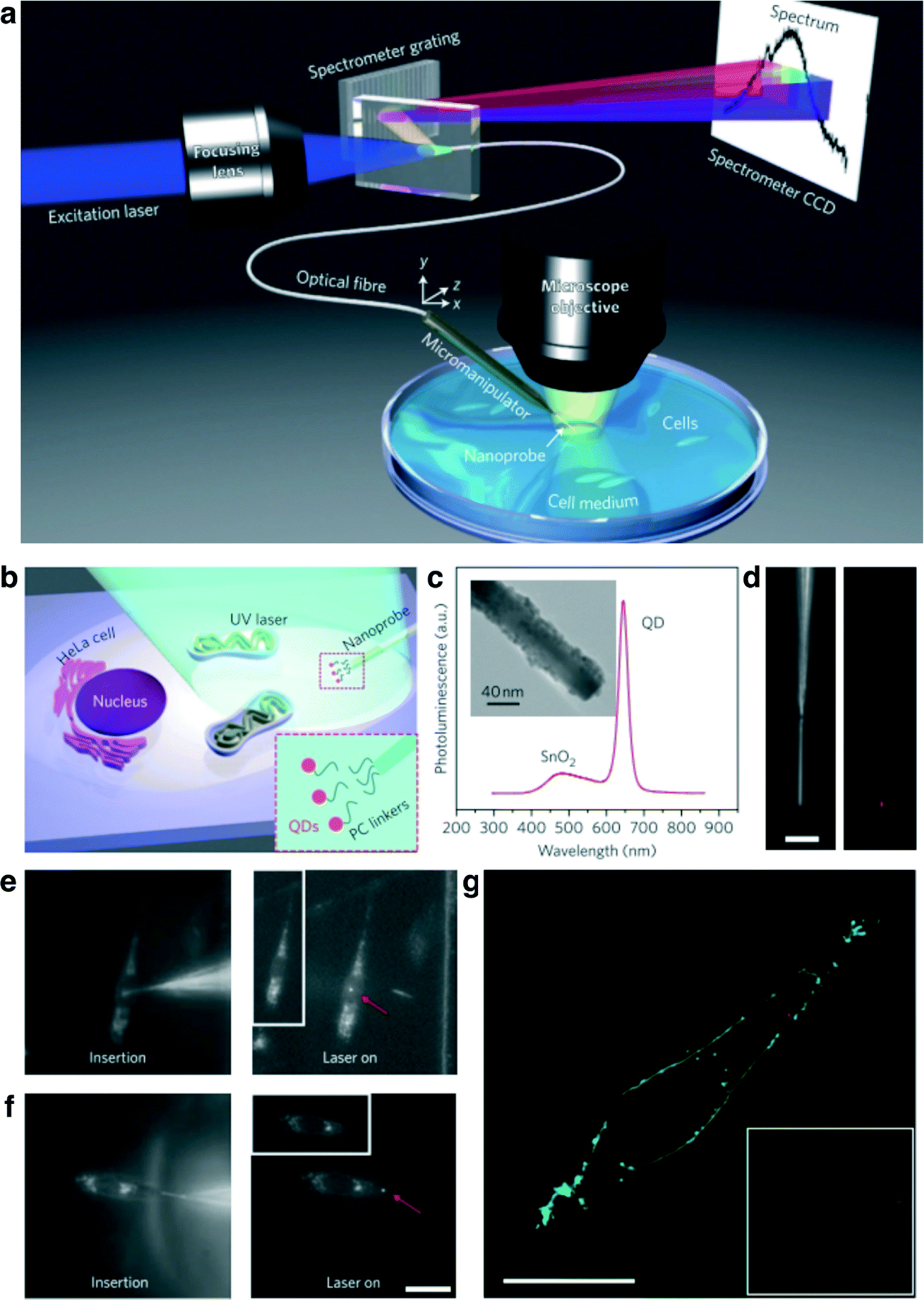 | ||
| Fig. 9 (a) Schematic illustration of the nanowire-based cell endoscope system. The nanowire endoscope, consisting of a nanowire waveguide fixed on the tapered tip of an optical fiber, can be inserted into a single living cell at designated positions using a three-axis micromanipulating system for spot delivery of payloads. The nanowire endoscope can be optically coupled to either an excitation laser to function as a local light source for molecular imaging or a spectrometer to collect local optical signals. CCD, charge-coupled device. (b) Schematic of the spatiotemporal delivery of quantum dots (QDs) into a living cell using a photoactivatable nanowire endoscope. Inset: QDs were conjugated to the nanowire by photocleavable (PC) linkers. (c) Photoluminescence spectrum of a QD (emission, 655 nm)-conjugated SnO2 nanowire endoscope excited with a focused HeCd laser (325 nm). Inset: transmission electron microscopy (TEM) image of the QD-conjugated SnO2 nanoprobe. Nanowires with smaller sizes than the average nanowire endoscopes had better contrast and were selected for TEM imaging. (d) Dark-field (left) and fluorescence (right) images of the QD-conjugated SnO2 nanowire endoscope. (e, f) Dark-field images showing a nanowire endoscope inserted into a cell nucleus (e, left) and cytoplasm (f, left), and fluorescence images taken after UV irradiation (325 nm, 1 min) was focused on the nanoprobe tip, showing QD fluorescence in the cell nucleus region (e, right) and in the cell cytoplasm (f, right) under 442 nm laser excitation. Dark-field illumination was left on when the fluorescence image was captured to show the cell outline. Insets in (e) and (f): dark-field images of the two cells when the 442 nm excitation laser was turned off. A 532 nm long-pass filter was used to screen the excitation laser for fluorescence imaging. Magnifications for (e) and (f) are the same. (g) Fluorescence confocal image of a HeLa cell, showing that the nanoprobe has delivered the QDs (red dot in the cytoplasm) within the cell membrane (green), which were labelled with an Alexa Fluor 488 conjugate of wheat germ agglutinin. A 488 nm laser was used to excite both the cell membrane stain and the QDs. Inset: dark-field image of the cell during QD delivery with a nanowire endoscope. Scale bars in (d), (f), and (g), 20 μm. Modified and reprinted with permission.91 Copyright 2012 Nature Publishing Group. | ||
4. Conclusions and perspectives
Researchers have successfully used various technical approaches to develop nanowires for bio-applications in molecular to cellular levels. In this review, we summarized the critical results, obtained using nanowire structures as a platform, for detection and analysis in bioanalytical chemistry and medical diagnostics. Nanowires have been integrated with microchannels, providing a pathway from the macroscale to nanoscale that allows researchers to observe and analyze target molecules such as DNA, RNA, proteins and CTCs. Semiconductor nanowires, which serve as critical sensing elements due to their high sensitivity and short response time, have been integrated with as FET by utilizing top-down fabrication techniques. These advantages allowed a SiNW-FET to be coupled with nanopores for DNA detection, which is a promising approach for high throughput DNA sequencing. Another benefit of nanowires is their very small diameter size with a high aspect ratio; this enabled researchers to use nanowires as a probe tip to stimulate and record changes of electrical signals in living cells. Moreover, the SiNW-FET can be merged with a synthesized tissue to fabricate a flexible nanowire nanoelectronic scaffold (nanoES). The NanoES is a paradigm shift for nanodevices and holds the promise to create a cyborg skin, which would sense chemical and electrical changes. Nanowires were also used as biological optical sensors; nanowire fluorescence optical imaging was done within cells for identification and within a nanowire structure array for SERS detection. SnO2 nanowires were demonstrated to be applicable as an optical waveguide and as a tool to deliver a cargo of quantum dots into a cell without damaging the cell. These dramatic improvements of nanowire structures allow the development of a new level of bioanalytical chemistry and medical diagnostics that will bring about a new age of nanotechnology with widespread use of nanowires for bio-applications.Competing financial interests
The authors declare no competing financial interests.Acknowledgements
This research was supported by the ImPACT Program of the Council for Science, Technology and Innovation (Cabinet Office, Government of Japan), a JSPS Grant-in-Aid for Scientific Research (A) 24241050, a Grant-in-Aid for Scientific Research on Innovative Areas “Nanomedicine Molecular Science” No. 26107709 from the Ministry of Education, Culture, Sports, Science, and Technology (MEXT), Japan, and PRESTO, JST.References
- J. T. Hu, T. W. Odom and C. M. Lieber, Acc. Chem. Res., 1999, 32, 435–445 CrossRef CAS.
- Y. N. Xia, P. D. Yang, Y. G. Sun, Y. Y. Wu, B. Mayers, B. Gates, Y. D. Yin, F. Kim and Y. Q. Yan, Adv. Mater., 2003, 15, 353–389 CrossRef CAS.
- N. Wang, Y. Cai and R. Q. Zhang, Mater. Sci. Eng., R, 2008, 60, 1–51 CrossRef.
- A. M. Morales and C. M. Lieber, Science, 1998, 279, 208–211 CrossRef CAS PubMed.
- L. Vayssieres, Adv. Mater., 2003, 15, 464–466 CrossRef CAS.
- Y. He, T. Yanagida, K. Nagashima, F. W. Zhuge, G. Meng, B. Xu, A. Klamchuen, S. Rahong, M. Kanai, X. M. Li, M. Suzuki, S. Kai and T. Kawai, J. Phys. Chem. C, 2013, 117, 1197–1203 CrossRef CAS.
- R. Laocharoensuk, K. Palaniappan, N. A. Smith, R. M. Dickerson, D. J. Werder, J. K. Baldwin and J. A. Hollingsworth, Nat. Nanotechnol., 2013, 8, 660–666 CrossRef CAS PubMed.
- X. D. Wang, C. J. Summers and Z. L. Wang, Nano Lett., 2004, 4, 423–426 CrossRef CAS PubMed.
- G. Meng, T. Yanagida, K. Nagashima, T. Yanagishita, M. Kanai, K. Oka, A. Klamchuen, S. Rahong, M. Horprathum, B. Xu, F. Zhuge, Y. He, H. Masuda and T. Kawai, RSC Adv., 2012, 2, 10618–10623 RSC.
- M. L. Zhang, K. Q. Peng, X. Fan, J. S. Jie, R. Q. Zhang, S. T. Lee and N. B. Wong, J. Phys. Chem. C, 2008, 112, 4444–4450 CrossRef CAS.
- W. Chern, K. Hsu, I. S. Chun, B. P. de Azeredo, N. Ahmed, K. H. Kim, J. M. Zuo, N. Fang, P. Ferreira and X. L. Li, Nano Lett., 2010, 10, 1582–1588 CrossRef CAS PubMed.
- Z. P. Huang, X. X. Zhang, M. Reiche, L. F. Liu, W. Lee, T. Shimizu, S. Senz and U. Gosele, Nano Lett., 2008, 8, 3046–3051 CrossRef CAS PubMed.
- C. X. Xiang, S. C. Kung, D. K. Taggart, F. Yang, M. A. Thompson, A. G. Guell, Y. A. Yang and R. M. Penner, ACS Nano, 2008, 2, 1939–1949 CrossRef CAS PubMed.
- H. D. Tong, S. Chen, W. G. van der Wiel, E. T. Carlen and A. van den Berg, Nano Lett., 2009, 9, 1015–1022 CrossRef CAS PubMed.
- C. X. Xiang, M. A. Thompson, F. Yang, E. J. Menke, L. M. C. Yang and R. M. Penner, Phys. Status Solidi C, 2008, 5, 3503–3505 CrossRef CAS.
- Y. P. Dan, K. Seo, K. Takei, J. H. Meza, A. Javey and K. B. Crozier, Nano Lett., 2011, 11, 2527–2532 CrossRef CAS PubMed.
- M. C. McAlpine, H. Ahmad, D. W. Wang and J. R. Heath, Nat. Mater., 2007, 6, 379–384 CrossRef CAS PubMed.
- M. M. Arafat, B. Dinan, S. A. Akbar and A. S. M. A. Haseeb, Sensors, 2012, 12, 7207–7258 CrossRef CAS PubMed.
- V. Kumar, S. Sen, K. P. Muthe, N. K. Gaur, S. K. Gupta and J. V. Yakhmi, Sens. Actuators, B, 2009, 138, 587–590 CrossRef CAS.
- L. B. Hu, H. Wu and Y. Cui, MRS Bull., 2011, 36, 760–765 CrossRef CAS.
- W. Lu and C. M. Lieber, Nat. Mater., 2007, 6, 841–850 CrossRef CAS PubMed.
- D. Vanmaekelbergh and L. K. van Vugt, Nanoscale, 2011, 3, 2783–2800 RSC.
- E. Garnett and P. D. Yang, Nano Lett., 2010, 10, 1082–1087 CrossRef CAS PubMed.
- W. Lu and C. M. Lieber, J. Phys. D: Appl. Phys., 2006, 39, R387–R406 CrossRef CAS.
- M. Law, J. Goldberger and P. D. Yang, Annu. Rev. Mater. Res., 2004, 34, 83–122 CrossRef CAS.
- Y. Cui, Q. Q. Wei, H. K. Park and C. M. Lieber, Science, 2001, 293, 1289–1292 CrossRef CAS PubMed.
- F. A. Aldaye, A. L. Palmer and H. F. Sleiman, Science, 2008, 321, 1795–1799 CrossRef CAS PubMed.
- X. P. A. Gao, G. F. Zheng and C. M. Lieber, Nano Lett., 2010, 10, 547–552 CrossRef CAS PubMed.
- I. Yoon, T. Kang, W. Choi, J. Kim, Y. Yoo, S. W. Joo, Q. H. Park, H. Ihee and B. Kim, J. Am. Chem. Soc., 2009, 131, 758–762 CrossRef CAS PubMed.
- M. S. Faber, R. Dziedzic, M. A. Lukowski, N. S. Kaiser, Q. Ding and S. Jin, J. Am. Chem. Soc., 2014, 136, 10053–10061 CrossRef CAS PubMed.
- A. Afzal, N. Cioffi, L. Sabbatini and L. Torsi, Sens. Actuators, B, 2012, 171, 25–42 CrossRef.
- C. Mayousse, C. Celle, A. Fraczkiewicz and J. P. Simonato, Nanoscale, 2015, 7, 2107–2115 RSC.
- F. X. Shen, M. M. Tan, Z. X. Wang, M. S. Yao, Z. Q. Xu, Y. Wu, J. D. Wang, X. F. Guo and T. Zhu, Environ. Sci. Technol., 2011, 45, 7473–7480 CrossRef CAS PubMed.
- C. F. Pan, J. Luo and J. Zhu, Nano Res., 2011, 4, 1099–1109 CrossRef.
- X. Wang and C. S. Ozkan, Nano Lett., 2008, 8, 398–404 CrossRef CAS PubMed.
- S. W. Lee, W. J. Chang, R. Bashir and Y. M. Koo, Biotechnol. Bioprocess Eng., 2007, 12, 185–199 CrossRef CAS.
- J. H. Chua, R. E. Chee, A. Agarwal, S. M. Wong and G. J. Zhang, Anal. Chem., 2009, 81, 6266–6271 CrossRef CAS PubMed.
- E. A. Schilling, A. E. Kamholz and P. Yager, Anal. Chem., 2002, 74, 1798–1804 CrossRef CAS PubMed.
- M. V. Berezovski, T. W. Mak and S. N. Krylov, Anal. Bioanal. Chem., 2007, 387, 91–96 CrossRef CAS PubMed.
- S. W. Lee and Y. C. Tai, Sens. Actuators, A, 1999, 73, 74–79 CrossRef CAS.
- B. Gabriel and J. Teissie, Biophys. J., 1999, 76, 2158–2165 CrossRef CAS PubMed.
- W. Kim, J. K. Ng, M. E. Kunitake, B. R. Conklin and P. D. Yang, J. Am. Chem. Soc., 2007, 129, 7228–7229 CrossRef CAS PubMed.
- J. Kim, M. Hegde, S. H. Kim, T. K. Wood and A. Jayaraman, Lab Chip, 2012, 12, 1157–1163 RSC.
- H. Y. So, K. Lee, N. Murthy and A. P. Pisano, ACS Appl. Mater. Interfaces, 2014, 6, 20693–20699 Search PubMed.
- T. Yasui, N. Kaji, M. R. Mohamadi, Y. Okamoto, M. Tokeshi, Y. Horiike and Y. Baba, ACS Nano, 2011, 5, 7775–7780 CrossRef CAS PubMed.
- N. Kaji, Y. Tezuka, Y. Takamura, M. Ueda, T. Nishimoto, H. Nakanishi, Y. Horiike and Y. Baba, Anal. Chem., 2004, 76, 15–22 CrossRef CAS PubMed.
- T. Yasui, N. Kaji, R. Ogawa, S. Hashioka, M. Tokeshi, Y. Horiike and Y. Baba, Nano Lett., 2015, 15, 3445–3451 CrossRef CAS PubMed.
- T. Yasui, N. Kaji, R. Ogawa, S. Hashioka, M. Tokeshi, Y. Horiike and Y. Baba, Anal. Chem., 2011, 83, 6635–6640 CrossRef CAS PubMed.
- S. G. Park, D. W. Olson and K. D. Dorfman, Lab Chip, 2012, 12, 1463–1470 RSC.
- N. Minc, C. Futterer, K. D. Dorfman, A. Bancaud, C. Gosse, C. Goubault and J. L. Viovy, Anal. Chem., 2004, 76, 3770–3776 CrossRef CAS PubMed.
- J. Chen, J. Li and Y. Sun, Lab Chip, 2012, 12, 1753–1767 RSC.
- P. S. Doyle, J. Bibette, A. Bancaud and J. L. Viovy, Science, 2002, 295, 2237 CrossRef CAS PubMed.
- M. Tabuchi, M. Ueda, N. Kaji, Y. Yamasaki, Y. Nagasaki, K. Yoshikawa, K. Kataoka and Y. Baba, Nat. Biotechnol., 2004, 22, 337–340 CrossRef CAS PubMed.
- S. Rahong, T. Yasui, T. Yanagida, K. Nagashima, M. Kanai, A. Klamchuen, G. Meng, Y. He, F. Zhuge, N. Kaji, T. Kawai and Y. Baba, Sci. Rep., 2014, 4, 5252–5259 CrossRef CAS PubMed.
- S. Rahong, T. Yasui, T. Yanagida, K. Nagashima, M. Kanai, G. Meng, Y. He, F. W. Zhuge, N. Kaji, T. Kawai and Y. Baba, Sci. Rep., 2015, 5, 10584–10592 CrossRef CAS PubMed.
- S. Rahong, T. Yasui, T. Yanagida, K. Nagashima, M. Kanai, G. Meng, Y. He, F. W. Zhuge, N. Kaji, T. Kawai and Y. Baba, Anal. Sci., 2015, 31, 153–157 CrossRef CAS PubMed.
- A. Meller and D. Branton, Electrophoresis, 2002, 23, 2583–2591 CrossRef CAS PubMed.
- J. B. Heng, A. Aksimentiev, C. Ho, P. Marks, Y. V. Grinkova, S. Sligar, K. Schulten and G. Timp, Nano Lett., 2005, 5, 1883–1888 CrossRef CAS PubMed.
- J. Lagerqvist, M. Zwolak and M. Di Ventra, Nano Lett., 2006, 6, 779–782 CrossRef CAS PubMed.
- C. Dekker, Nat. Nanotechnol., 2007, 2, 209–215 CrossRef CAS PubMed.
- B. M. Venkatesan and R. Bashir, Nat. Nanotechnol., 2011, 6, 615–624 CrossRef CAS PubMed.
- S. L. Levy and H. G. Craighead, Chem. Soc. Rev., 2010, 39, 1133–1152 RSC.
- M. Napoli, J. C. T. Eijkel and S. Pennathur, Lab Chip, 2010, 10, 957–985 RSC.
- V. R. S. S. Mokkapati, V. Di Virgilio, C. Shen, J. Mollinger, J. Bastemeijer and A. Bossche, Lab Chip, 2011, 11, 2711–2719 RSC.
- S. W. Kowalczyk, D. B. Wells, A. Aksimentiev and C. Dekker, Nano Lett., 2012, 12, 1038–1044 CrossRef CAS PubMed.
- S. W. Kowalczyk and C. Dekker, Nano Lett., 2012, 12, 4159–4163 CrossRef CAS PubMed.
- K. D. Dorfman, Rev. Mod. Phys., 2010, 82, 2903–2947 CrossRef CAS.
- C. Bustamante, J. F. Marko, E. D. Siggia and S. Smith, Science, 1994, 265, 1599–1600 CrossRef CAS PubMed.
- T. Yasui, S. Rahong, K. Motoyama, T. Yanagida, Q. Wu, N. Kaji, M. Kanai, K. Doi, K. Nagashima, M. Tokeshi, M. Taniguchi, S. Kawano, T. Kawai and Y. Baba, ACS Nano, 2013, 7, 3029–3035 CrossRef CAS PubMed.
- M. Hosokawa, T. Hayata, Y. Fukuda, A. Arakaki, T. Yoshino, T. Tanaka and T. Matsunaga, Anal. Chem., 2010, 82, 6629–6635 CrossRef CAS PubMed.
- U. Dharmasiri, S. K. Njoroge, M. A. Witek, M. G. Adebiyi, J. W. Kamande, M. L. Hupert, F. Barany and S. A. Soper, Anal. Chem., 2011, 83, 2301–2309 CrossRef CAS PubMed.
- S. L. Stott, C. H. Hsu, D. I. Tsukrov, M. Yu, D. T. Miyamoto, B. A. Waltman, S. M. Rothenberg, A. M. Shah, M. E. Smas, G. K. Korir, F. P. Floyd, A. J. Gilman, J. B. Lord, D. Winokur, S. Springer, D. Irimia, S. Nagrath, L. V. Sequist, R. J. Lee, K. J. Isselbacher, S. Maheswaran, D. A. Haber and M. Toner, Proc. Natl. Acad. Sci. U. S. A., 2010, 107, 18392–18397 CrossRef CAS PubMed.
- M. Lin, J. F. Chen, Y. T. Lu, Y. Zhang, J. Z. Song, S. Hou, Z. F. Ke and H. R. Tseng, Acc. Chem. Res., 2014, 47, 2941–2950 CrossRef CAS PubMed.
- Z. F. Ke, M. Lin, J. F. Chen, J. S. Choi, Y. Zhang, A. Fong, A. J. Liang, S. F. Chen, Q. Y. Li, W. F. Fang, P. S. Zhang, M. A. Garcia, T. Lee, M. Song, H. A. Lin, H. C. Zhao, S. C. Luo, S. Hou, H. H. Yu and H. R. Tseng, ACS Nano, 2015, 9, 62–70 CrossRef CAS PubMed.
- Q. L. Shen, L. Xu, L. B. Zhao, D. X. Wu, Y. S. Fan, Y. L. Zhou, W. H. OuYang, X. C. Xu, Z. Zhang, M. Song, T. Lee, M. A. Garcia, B. Xiong, S. Hou, H. R. Tseng and X. H. Fang, Adv. Mater., 2013, 25, 2368–2373 CrossRef CAS PubMed.
- Y. T. Lu, L. B. Zhao, Q. L. Shen, M. A. Garcia, D. X. Wu, S. Hou, M. Song, X. C. Xu, W. H. OuYang, W. W. L. OuYang, J. Lichterman, Z. Luo, X. Xuan, J. T. Huang, L. W. K. Chung, M. Rettig, H. R. Tseng, C. Shao and E. M. Posadas, Methods, 2013, 64, 144–152 CrossRef CAS PubMed.
- N. P. Dasgupta, J. W. Sun, C. Liu, S. Brittman, S. C. Andrews, J. Lim, H. W. Gao, R. X. Yan and P. D. Yang, Adv. Mater., 2014, 26, 2137–2184 CrossRef CAS PubMed.
- K. Balasubramanian, Biosens. Bioelectron., 2010, 26, 1195–1204 CrossRef CAS PubMed.
- S. Mao, K. H. Yu, G. H. Lu and J. H. Chen, Nano Res., 2011, 4, 921–930 CrossRef.
- D. Sarkar, W. Liu, X. J. Xie, A. C. Anselmo, S. Mitragotri and K. Banerjee, ACS Nano, 2014, 8, 3992–4003 CrossRef CAS PubMed.
- C. P. Chen, A. Ganguly, C. Y. Lu, T. Y. Chen, C. C. Kuo, R. S. Chen, W. H. Tu, W. B. Fischer, K. H. Chen and L. C. Chen, Anal. Chem., 2011, 83, 1938–1943 CrossRef CAS PubMed.
- G. F. Zheng, F. Patolsky, Y. Cui, W. U. Wang and C. M. Lieber, Nat. Biotechnol., 2005, 23, 1294–1301 CrossRef CAS PubMed.
- P. Xie, Q. H. Xiong, Y. Fang, Q. Qing and C. M. Lieber, Nat. Nanotechnol., 2012, 7, 119–125 CrossRef CAS PubMed.
- X. J. Duan, R. X. Gao, P. Xie, T. Cohen-Karni, Q. Qing, H. S. Choe, B. Z. Tian, X. C. Jiang and C. M. Lieber, Nat. Nanotechnol., 2012, 7, 174–179 CrossRef CAS PubMed.
- J. T. Robinson, M. Jorgolli, A. K. Shalek, M. H. Yoon, R. S. Gertner and H. Park, Nat. Nanotechnol., 2012, 7, 180–184 CrossRef CAS PubMed.
- Z. Jiang, Q. Qing, P. Xie, R. X. Gao and C. M. Lieber, Nano Lett., 2012, 12, 1711–1716 CrossRef CAS PubMed.
- Q. Qing, Z. Jiang, L. Xu, R. X. Gao, L. Q. Mai and C. M. Lieber, Nat. Nanotechnol., 2014, 9, 142–147 CrossRef CAS PubMed.
- B. Z. Tian, J. Liu, T. Dvir, L. H. Jin, J. H. Tsui, Q. Qing, Z. G. Suo, R. Langer, D. S. Kohane and C. M. Lieber, Nat. Mater., 2012, 11, 986–994 CrossRef CAS PubMed.
- J. A. Huang, Y. Q. Zhao, X. J. Zhang, L. F. He, T. L. Wong, Y. S. Chui, W. J. Zhang and S. T. Lee, Nano Lett., 2013, 13, 5039–5045 CrossRef CAS PubMed.
- K. Adolfsson, H. Persson, J. Wallentin, S. Oredsson, L. Samuelson, J. O. Tegenfeldt, M. T. Borgstrom and C. N. Prinz, Nano Lett., 2013, 13, 4728–4732 CrossRef CAS PubMed.
- R. X. Yan, J. H. Park, Y. Choi, C. J. Heo, S. M. Yang, L. P. Lee and P. D. Yang, Nat. Nanotechnol., 2012, 7, 191–196 CrossRef CAS PubMed.
| This journal is © The Royal Society of Chemistry 2016 |