
Glow discharge optical emission spectrometry elemental mapping with restrictive anode array masks†
Marcel
Kroschk
,
John
Usala
,
Trevor
Addesso
and
Gerardo
Gamez
*
Texas Tech University, Department of Chemistry and Biochemistry, Box 41061, Lubbock, TX 7940-1061, USA. E-mail: Gerardo.Gamez@ttu.edu
First published on 13th August 2015
Abstract
Large-area surface elemental mapping is highly beneficial for a multitude of applications in fields from materials science to biology. Current typical methods, however, suffer from long acquisition times. Glow Discharge Optical Emission Spectrometry (GDOES), under pulsed-power and higher pressure operation, exhibits a great potential for ultrahigh throughput chemical imaging of large surface area samples. Up until now, various proof-of-principle studies of GDOES elemental mapping have only been applied to smaller surface area samples. Thus, there is a need for development of GDOES systems that allow for analysis of large area samples. Here, the design of different GD configurations for large area sample (10 cm diameter) analysis is investigated as a function of operating conditions such as pressure (133–4000 Pa), applied power (up to 5 kW), and pulsing. An open face electrode (OFE) design generated undesirable heterogeneous plasma at the higher pressures required for achieving spatial resolution. On the other hand, a restrictive anode array mask (RAAM) design provided notable homogeneity within the same pressure range and enabled the lateral resolution of 1 mm diameter silver inclusions embedded in copper. RAAMS were designed varying thickness (3 mm and 12 mm), aperture size (4, 6, 8 mm), geometry, and grounding. Also, as the section sputtered is restricted to the area covered by the apertures, the RAAM provides the opportunity for subsequent analysis of the unsputtered regions via alternative methods. In addition, the RAAM permits higher power densities to be achieved within the limitations of the power supply. These findings help to pave the way for exploiting the full potential of GDOES and its ultrahigh throughput elemental mapping of large surface area samples.
Introduction
Glow Discharge Optical Emission Spectrometry (GDOES) has become renowned for the ability to provide direct chemical surface analysis and depth profiling of solid samples.1–7 In its current commercially available form, the attributes of GDOES include a broad dynamic range, good limits of detection, simultaneous multi-elemental analysis, excellent depth resolution (in the order of nanometers), as well as fast analysis (seconds to minutes).1,4,8,9It was not until recent studies, however, that exploration rekindled in expanding the lateral resolution of this method,2,4,10–15 which historically had been limited to a few millimeters or the size of the sputtered area. In 1995 Winchester and Salit14 proposed a design that enabled them to collect emissions from multiple direct current discharges located at different positions on the same sample, which yielded resolution on the order of several millimeters. Later that year Hoffmann and Ehrlich15 showed that the lateral intensity distribution of GD emissions above the sample is influenced by the sample heterogeneity.4 In more recent studies it was shown that the use of pulsed DC or RF power in conjunction with higher vacuum pressures can result in laterally resolved analysis within the sputtered area.1,11 In a particular set of studies Gamez et al.1 developed a GD lamp that could analyze up to 28 mm diameter surfaces, and utilizing pulsed RF-power and pressures as high as 3870 Pa they achieved elemental mapping with lateral resolutions in the order of 0.667 line pairs per mm. During a similar study Webb et al. developed a GD lamp which allowed for analysis of a 15 mm diameter sample surface using pulsed DC-power, and they found that the FWHM emission intensity profile above a 1 mm Cu insertion to be accurate to within 100 μm.
In their original study Gamez et al.1 developed a method of analysis for proteins on blotting membranes by using a silver-enhanced colloidal gold stain. Another proof-of-concept study showed the potential of GDOES elemental mapping for thin film materials combinatorial libraries11 on a GD lamp allowing analysis of 8 mm diameter surfaces. Elemental maps of these samples were obtained orders of magnitude faster than would have been the case using traditional methods.11 Although these proof-of-concept studies showed potential applications and advantages of GDOES elemental mapping, the samples in these studies were designed smaller than is the norm because the GD lamps utilized were not large enough to accommodate typical size samples which is more in the order of 100 mm diameter or larger for combinatorial libraries and protein gels.16–18 In order to fully harness the potential of GDOES elemental mapping it is necessary to develop a GD lamp capable of accommodating samples with the same dimensions as those relevant to samples of interest.
Large GD sources have been developed to accomplish other tasks, such as cleaning the large optics found in observatories.19,20 Voronov et al.21 developed a GD source with which they could analyze samples as large as 8 cm diameter, but found that the source had limitation of power density and pressure.21 Furthermore a later study by the authors highlighted heterogeneities and spot patterns within the discharge plasma that became amplified under desired elemental mapping conditions.22 Herein, the development of a GD lamp to accommodate large diameter samples is presented. The effects of operating conditions, including pressure and RF-power levels, as well as different anode/cathode geometries and grounding schemes, on plasma stability and spatial resolution are explored.
Experimental
Glow discharge chamber
A custom-built glow discharge chamber designed for 10 cm samples was used. The dimensions of the cylindrical chamber (53.2 cm i.d. × 55.5 cm) are larger relative to traditional GD chambers to maximize the anode-to-cathode surface area, which is critical for allowing the bias voltage formation at the cathode in RF-power mode. The chamber rested on its length with the sample mount (Fig. 1) and a 10 cm viewing window situated on axis at each opposite end of the cylindrical chamber end caps. The sample mount housed a MACOR insulator ring, sample, and brass backing-electrode. The electrode was inserted into a plastic sleeve with two O-rings. A grounded cover with an insulated insert enclosed the entire sample mount setup.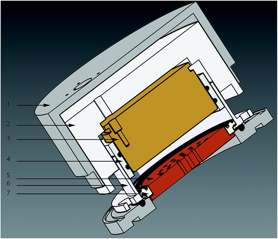 | ||
| Fig. 1 Schematic of GDOES sample mount: (1) grounded aluminum cover, (2) PTFE insert, (3) brass electrode, (4) PTFE sleeve, (5) restrictive anode array mask (RAAM), (6) PTFE sample holder, (7) MACOR insulator ring. | ||
Each copper restrictive anode array mask (RAAM) was mounted onto the insulator such that a distance of 200 μm from the sample surface to the mask was maintained as depicted in Fig. 1. RAAMs were designed varying the following parameters: geometric pattern of the array (hexagonal vs. concentric circle), aperture diameter (4 mm, 6 mm, 8 mm), aperture number (1, 7, 37), mask thickness (3 mm and 12 mm), and mask grounding to the chamber (single connection 0.75 mm copper wire, single connection flat 5/8′′ tinned copper braid, and a tinned copper braid grounding collar). Argon gas of 99.999% purity (Praxair Inc., Danbury, CT, USA) was used. A range of pressure from 133 Pa to 3990 Pa was used and monitored with an MKS 925 MicroPirani vacuum transducer and an MKS series 900 controller (MKS, Andover, MA, USA). Typical flow rates of 0.1 to 0.4 SLPM were set with a Cole-Parmer model 32907-69 mass flow controller (Cole-Parmer, Vernon Hills, IL, USA). The chamber was held under vacuum with a Trivac D 25 B vacuum with an adjustable valve (Oerlikon, Cologne, Germany). An RF power range of 0 kW to 5 kW was applied with a cito 1350 RF generator and coupled to an agilo 1350w RF matching network (Comet, Stolberg-Vicht, Germany). The power supply was cooled with a Polystat Cole Palmer high capacity re-circulating chiller. The RF frequency was 13.56 MHz and the glow discharge was operated under pulsed power conditions including a 16 μs to 100 μs pulse duration with a 1 kHz pulse frequency.
Hyperspectral imaging system
Hyperspectral imaging was accomplished with a push broom method. The glow discharge light emission passed through a sequence of optics consisting of a magnifying lens (80 mm nominal focal length, 0.138 magnification), collimating lens (100 mm nominal focal length), 90° reflecting mirror and focusing lens (100 mm nominal focal length). The last two components were mounted on a motorized stage (Thorlabs model, Newton, New Jersey, USA). The triplet lenses were UV-VIS-IR Apochromats (Bernhard-Halle GmBH, Berlin, Germany) made from calcium fluoride and fused silica. The final lens focused the image onto the entrance slit of a Czerny-Turner-Schmidt Isoplane SCT 320 spectrograph (Princeton Instruments, Trenton, USA). The motorized stage was controlled by a Thorlabs TDC001 DC servo controller allowing the image to be scanned across the slit of the spectrograph without needing to move the spectrograph or the GD chamber. During acquisition times, the stage was set to continuous movement at 58 μm per second. The spectrograph had a 600 lines per mm grating with a 300 nm blaze and a 1024 × 1024 pixel (1![[thin space (1/6-em)]](https://www.rsc.org/images/entities/char_2009.gif) :1 Fiber optic taper magnification and 13.3 × 13.3 mm effective active area of CCD) Andor iStar ICCD Model 334T camera (Andor, Belfast, UK). The camera operated with 2 × 2 binning and a gain from 200 to 3200 to ensure a maximum intensity below saturation. The gate duration and gate delay were mostly 35 μs and 14.8 μs, respectively, and 100 acquisitions were accumulated on the CCD chip before the picture frame was transferred to the computer. The gate duration was reduced to 16 μs for the imaging of the target with silver inlay. The ICCD's pulse generator was utilized to control the entire experiment. Thus, the pulse generator sent the trigger to the power generator which allowed pulsing at the selected duty cycle.
:1 Fiber optic taper magnification and 13.3 × 13.3 mm effective active area of CCD) Andor iStar ICCD Model 334T camera (Andor, Belfast, UK). The camera operated with 2 × 2 binning and a gain from 200 to 3200 to ensure a maximum intensity below saturation. The gate duration and gate delay were mostly 35 μs and 14.8 μs, respectively, and 100 acquisitions were accumulated on the CCD chip before the picture frame was transferred to the computer. The gate duration was reduced to 16 μs for the imaging of the target with silver inlay. The ICCD's pulse generator was utilized to control the entire experiment. Thus, the pulse generator sent the trigger to the power generator which allowed pulsing at the selected duty cycle.
Automation was accomplished with a custom designed LabVIEW (National Instruments, Austin, TX, USA) program. It controlled camera settings, pulse generation, and stage parameters. A single scan consisted of 460 raw images, and each image corresponded to a single x-spatial position with the y-spatial dimension across the vertical axis and spectral dimension across the horizontal axis. Image J software (NIST, Bethesda, MD, USA) was used to extract monochromatic images from the hyperspectral data cubes collected. Monochromatic spatial images were obtained by integrating over 12 images of the spectral sequence. This corresponded to 12 pixels in the spectral dimension (0.124 nm per pixel) around the wavelength of interest. A custom designed Matlab (MathWorks, Natick, Ma, USA) program was used, instead of Image J, for samples containing Ag which also included a smile correction needed to completely resolve an the emission at 328.1 nm. The correction allowed for the same information to be obtained by integrating 4 pixels of the spectral sequence.
Resolution was measured with a USAF 1951 resolution target, illuminated with an LED lamp, at the position of the GD sample at 3.33 line pairs per mm (150 μm) horizontal resolution and 2 lpm (250 μm) vertical resolution. Wavelength calibration was performed with an Hg pen lamp (Pen-Ray, Upland, CA, USA). A flat field correction was performed by placing a custom built rectangular cell containing a broadband emitting chemiluminescent compound in the field of view. The flat field image was obtained and processed exactly as the experimental images. After a dark current subtraction was performed on the corresponding monochromatic flat field and experimental images, the flat field image was normalized and used to divide the experimental image.
Results and discussion
Open-faced 100 mm GD source
Initially a 100 mm open faced GD source design was characterized. Hyperspectral data cubes were constructed based on the emissions from the source at pressures between 267 and 1870 Pa and monochromatic images were extracted at 324.7 nm and 327.4 nm corresponding to the emission lines of copper. At low pressure (267 Pa) a typical GDOES emission profile was observed across the entire surface of the cathode (Fig. 2A & B). Typical emission intensity profiles have been reported to be higher in the axis of the discharge and lower at the edges.15 However as the pressure was increased the emission intensity profile was inverted, showing higher emission at the edges, furthermore the discharge began to form filaments between cathode and anode that originated near the edges of the cathode surface (Fig. 2C & D).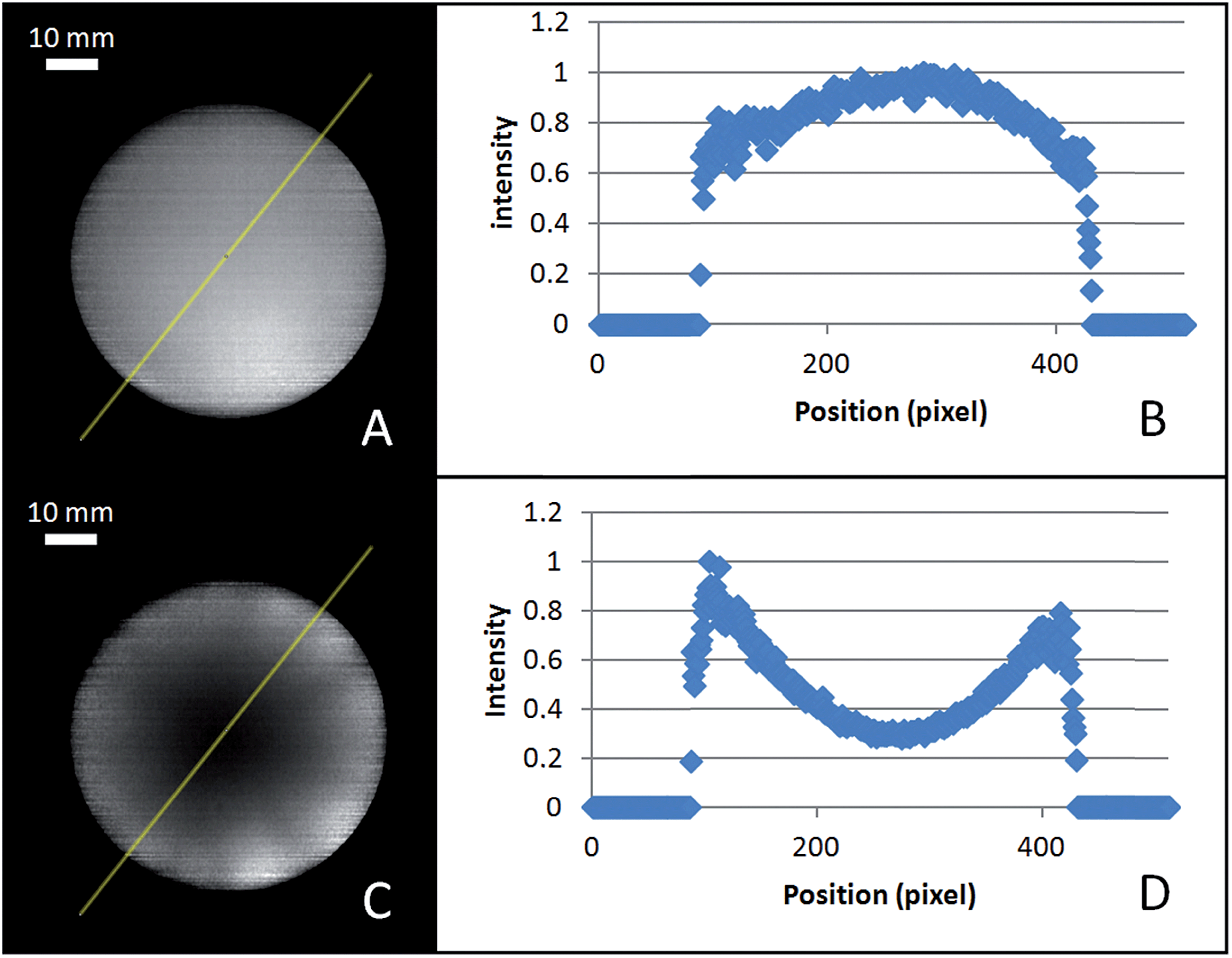 | ||
| Fig. 2 (A) Open face GDOES end-on emission image at 324.7 nm taken at 267 Pa with 2 watt mm−2. (B) Normalized intensity profile from the indicative yellow line in A. (C) Open face GDOES end-on emission image at 324.7 nm taken at 1870 Pa with 2 watt mm−2. (D) Normalized intensity profile from the indicative yellow line in C. | ||
The emission intensity ratios of 12 lateral positions to the center of the plasma were calculated to quantify the degree of change in the plasma homogeneity as a function of pressure (Fig. 3). Readings for the center were taken by averaging the intensity values of a 208 pixel area circle on the axis of the plasma. Readings for the lateral position were taken by averaging the intensity values of a 208 pixel area circle centered 20 mm from the axis of the plasma at 30 degree increments. Forward power began to fluctuate at pressures over 1870 Pa, causing a great build-up of heat in the cathode, thus becoming the upper practical pressure limit. It is evident from Fig. 2 and 3 that the GDOES emission becomes very heterogeneous as the pressure is increased to those required for pulsed-power GDOES elemental mapping. Voronov et al.22 also reported heterogeneities in the discharge of a GD chamber that could accommodate 80 mm diameter surface samples when operated at pressures required for obtaining laterally resolved information. They arrived at a 40 mm diameter GD chamber design with a monolithic anode where the heterogeneity is minimized but not eliminated and propose that the filaments are less likely to affect the sample's emission because they are confined to the edge of the sample. Our results and those by Voronov et al.22 show that an alternative approach to GDOES elemental mapping of large diameter samples is necessary.
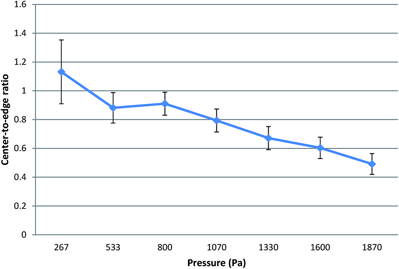 | ||
| Fig. 3 Center-to-edge ratio of the intensity values of the open face GDOES emission images at 324.7 nm and 2 watt mm−2, showing the increase in the overall emission intensity heterogeneity in the field-of-view of the plasma as a function of pressure. | ||
Restrictive anode mask
It is evident that having longer distances between the axis of the cathode and the anode leads to heterogeneities at higher pressures. Based on this we propose an alternative design that incorporates a restrictive anode array mask (RAAM) into the current set up. The idea is to have an anode plate separated from the cathode by less than 200 μm (130 μm ± 20 μm in our design) with an array of apertures with small diameters, i.e. <10 mm i.d.As such, a separate GD would be established in each aperture and one would be able to obtain elemental maps of large surfaces without the filamentous heterogeneities due to larger anode to cathode-axis distances. The RAAM approach is different from the GD array proposed by Winchester and Salit14 because the spatial resolution from the GDs with the RAAM is obtained through pulsed-power operation and higher pressures. In this manner, potential miniaturization limitations in the GD array design are also circumvented. The RAAM design not only brings the anode much closer to each cathode area, but it also does not sputter the whole surface area completely which leads to several advantages: (1) the pristine fraction of the sample surface can be analyzed by other methods, (2) larger samples can be analyzed while maintaining the same power density when compared to an “open face” cathode design. A restrictive mask with a single 8 mm aperture was constructed (Fig. 4) and it was verified that the anode mask could effectively restrict the glow discharge under elemental mapping experimental conditions. In addition, the voltage waveform was measured with a high voltage probe (Tektronix, 6015a) at the GD backing electrode. Fig. 4 shows the timing of the experiment from the main trigger to the delay in the voltage waveform and the time it takes for the DC bias voltage to develop.
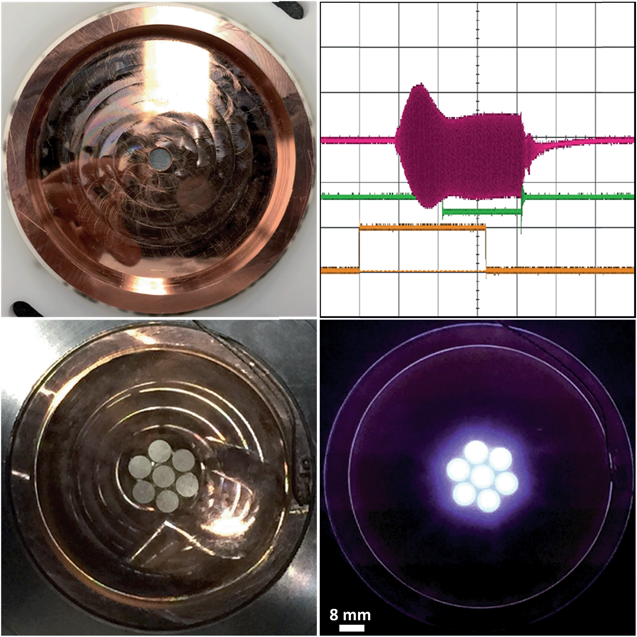 | ||
| Fig. 4 Single aperture restrictive anode mask (A). Oscilloscope traces (5 μs per div) of trigger pulse (yellow, lower trace, 5 V per div), ICCD gate (green, middle trace, 1 V per div), and GD voltage (red, upper trace, 0.5 V per div, 1000×) measured at backing electrode (B). Seven aperture restrictive anode array mask with GD power off (C) and GD power on (D). | ||
It was confirmed that no sputtering was evident anywhere except for the area exposed by the aperture. The RAM design was then altered to a restrictive anode array mask containing 7 apertures (Fig. 4). Initial tests showed that the emission intensity profile within each individual discharge was broad-bell shaped, as in typical GDOES, and that intensities were comparable between individual discharges (Fig. SI1†). The RAAM design was then expanded to span the entire FOV.
Array geometries
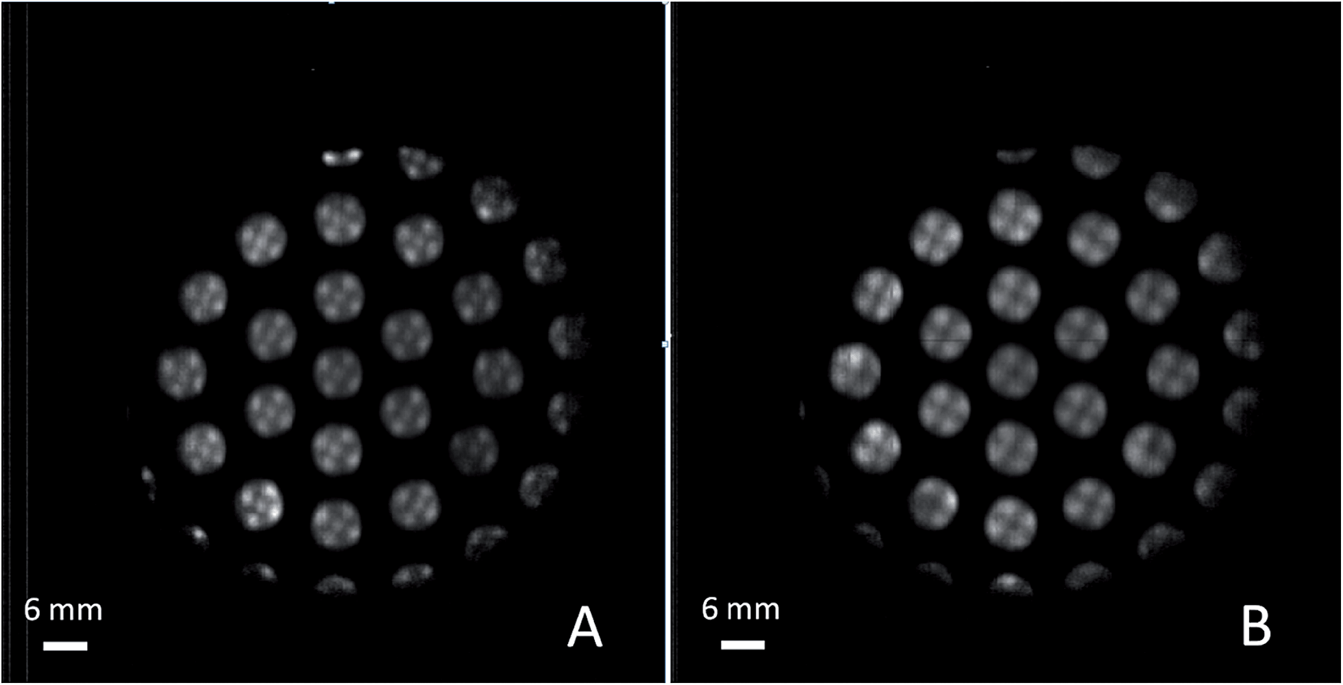
Studies were conducted to determine the effect of the geometry of the array on its performance. Two types of array geometries were investigated in order to cover the area of interest, a hexagonal design and a concentric circle design. In addition, different grounding schemes were tested: (a) a 0.75 mm wire connected to a single location near the edge of the RAAM (cf.Fig. 4), (b) a 12 mm grounding strip connected to a single location near the edge of the RAAM, and (c) a grounding collar made from a grounding strip connected all along the circumference of the RAAM. Each geometric pattern was then tested with each of the aforementioned grounding methods to determine which would provide the most uniform results. The single wire (data not shown) and the grounding strip connected to a single location on the RAAM resulted in higher glow intensity near the grounding point (Fig. 5A & C). It was found that the grounding collar method provided the most symmetric glow across the entire area of interest for both the hexagonal as well as the concentric circle array (Fig. 5B & D).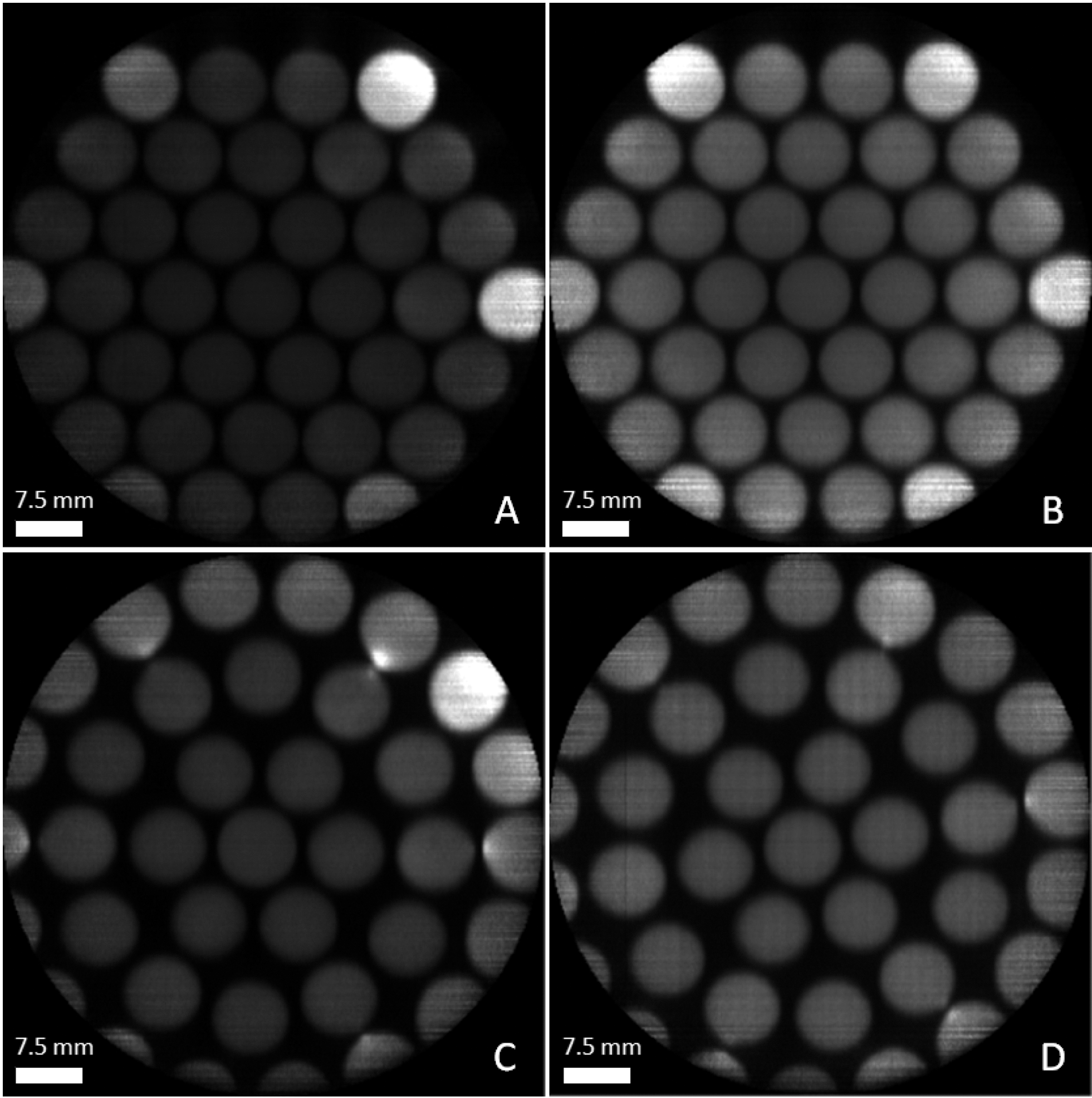 | ||
| Fig. 5 RAAM GDOES elemental mapping images with 3 mm thick masks, 8 mm apertures, 1330 Pa, 2 watt mm−2 at 324.7 nm. Hexagonal array with apertures spaced 0.5 mm apart and a 12 mm grounding strip in the top right corner (A) vs. grounding collar (B). Concentric circle array with apertures spaced 1 mm apart with a 12 mm grounding strip in the top right corner (C) or grounding collar (D). | ||
It is evident from Fig. 5B that the hexagonal geometry shows an increased intensity at the corner apertures, indicating that there may be a difference in potential closer to the point of grounding. It was noted that there was some inter-aperture emission, as can be seen in Fig. 5D. It was found that inter-aperture emissions increased at higher pressures, and as a result all subsequent studies were aimed to reduce the inter-aperture emission while maintaining a high level of homogeneity between individual plasmas.
RAAM thickness
As opposed to the open-face design, the RAAMs allowed operating the GD at higher pressures. Nevertheless, it was found that with increased pressures the inter-aperture plasma emission noted in a few places at lower pressure (see Fig. 6A) became more widespread and noticeable (see Fig. 6B). This observation led to a thicker mask design (12 mm vs. 3 mm).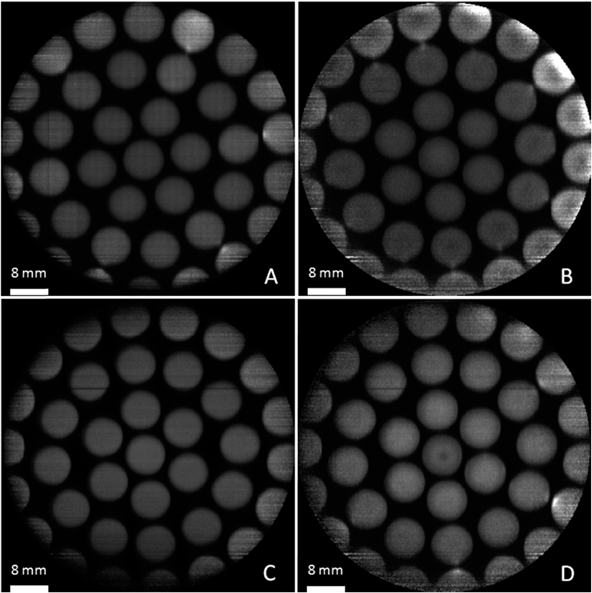 | ||
| Fig. 6 RAAM GDOES elemental mapping images from 8 mm aperture concentric circle arrays with a power density of 2 watt mm−2 at 324.7 nm: (A) 3 mm thick mask at 1330 Pa, (B) 3 mm thick mask at 2130 Pa, (C) 12 mm thick mask at 1330 Pa, (D) 12 mm thick mask at 2130 Pa. | ||
It can be seen in Fig. 6 that there is a complete elimination of inter-aperture emission at 1330 Pa when the mask thickness was changed from 3 mm to 12 mm. At higher pressures the inter-aperture emission was reduced but is still visible at pressure of 2130 Pa and above (Fig. 6D). However with the 12 mm thick mask it was possible to increase the range over which the glow discharge plasma could be operated up to 2930 Pa, in contrast to the 3 mm thick mask where the forward power was unstable at pressures over 2130 Pa. As pressures were increased further it was seen that, although inter-aperture emission was still reduced, some inhomogeneities appear above 2130 Pa. Nevertheless, overall plasma homogeneity, in terms of center-to-edge intensity ratio was much improved over the open face geometry (Fig. SI2†).
RAAM aperture size
RAAMs with 4 mm and 6 mm i.d. aperture diameters were designed in order to eliminate the intra-aperture heterogeneity. Additionally, to further decrease inter-aperture emissions, the inter-aperture distance was changed to 5 mm for the 4 mm aperture mask and 3 mm for the 6 mm mask. This also prevented the need to increase the number of apertures in order to cover the same field of view. Each of the masks were evaluated and compared to each other as well as to the open faced electrode. Fig. 7 compares the center-to-edge intensity ratios of the different aperture i.d. RAAMs, as well as the open face GD. It can be seen that the plasma homogeneity across the entire field of analysis is better with the RAAMs vs. the open face electrode.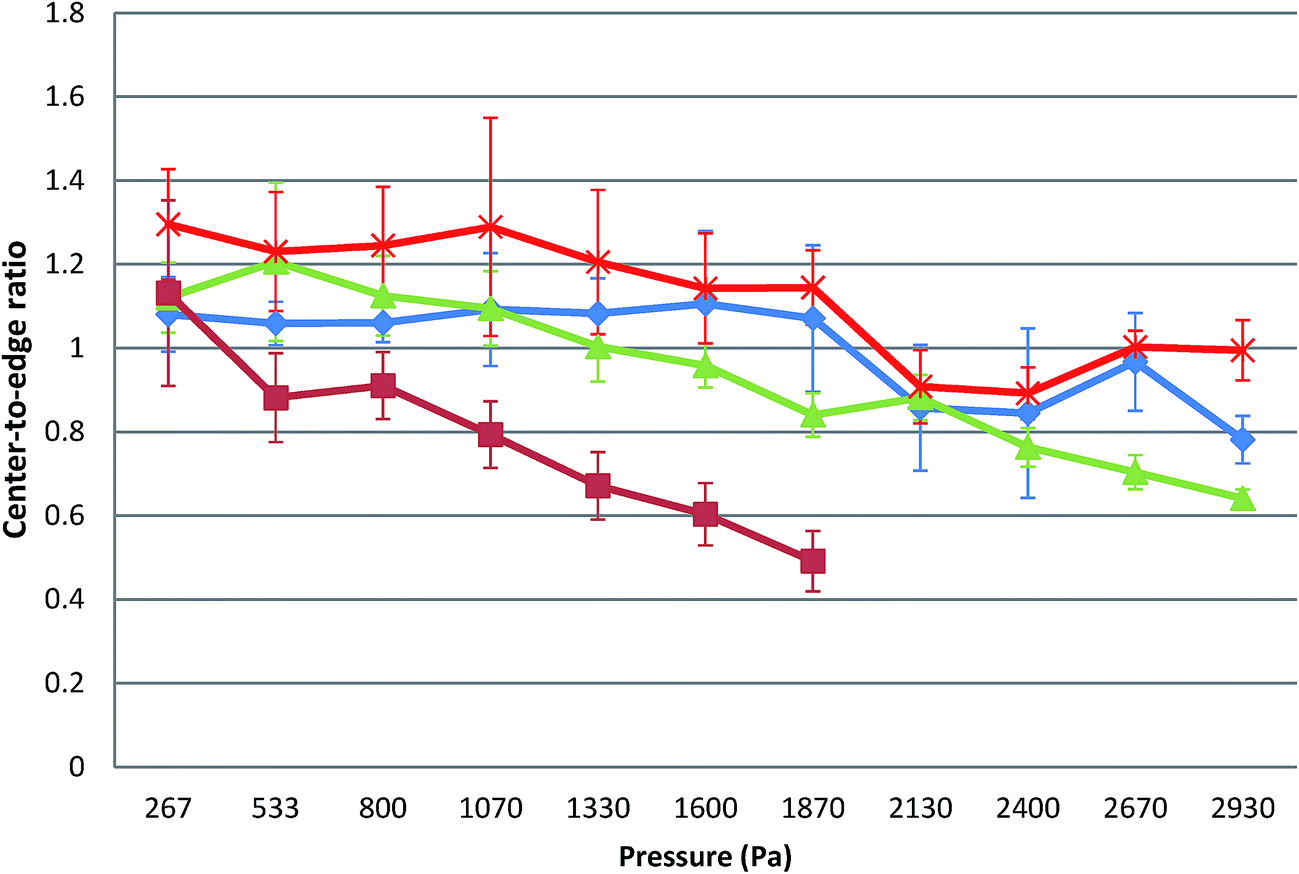 | ||
| Fig. 7 Center-to-edge ratio of the intensity at 324.7 nm corresponding to copper spectral emission of the open faced electrode (square marker) as well as the 4 mm (diamond marker), 6 mm (triangle marker), and 8 mm (x marker) RAAM's. | ||
At 1330 Pa all the RAAMs with different i.d. apertures showed very good homogeneity (Fig. SI3†). At 2400 Pa, however, an inspection of the images obtained for the 4 mm i.d. and 6 mm i.d. RAAMs show intra-aperture heterogeneities similar to those that had been found with the 8 mm RAAM (Fig. 8). Nevertheless, it was found that the increased inter-aperture distance had completely eliminated any inter-aperture emissions. Two types of inter-aperture heterogeneities are apparent: (1) bright spots (Fig. 8A–C) and (2) a series of dark regions (Fig. 8B & C). Thus, a study to determine the effect of power density on these heterogeneities was performed. The power supply upper power limit of 5000 watts restricted the power densities available at different i.d. aperture RAAMs: at 4 mm i.d. a range of 2 watt mm−2 to 7 watt mm−2 was studied, at 6 mm i.d. a range of 2 watt mm−2 to 4 watt mm−2, and at 8 mm i.d. only 2 watt mm−2 was studied. It is evident from Fig. 8 that as the power is increased from 2 watt mm−2 to 4 watt mm−2 on the 6 mm i.d. RAAM the intra-aperture inhomogeneities are eliminated.
 | ||
| Fig. 8 RAAM GDOES elemental mapping images at 2 watt mm−2, 324.7 nm, and 2400 Pa: (A) 4 mm aperture i.d. with 5 mm inter-aperture spacing, (B) 6 mm aperture i.d. with 3 mm inter-aperture spacing, (C) 8 mm aperture i.d. with 1 mm inter-aperture spacing. (D) 6 mm aperture i.d. with 3 mm inter-aperture spacing at 2130 Pa and 4 watt mm−2. | ||
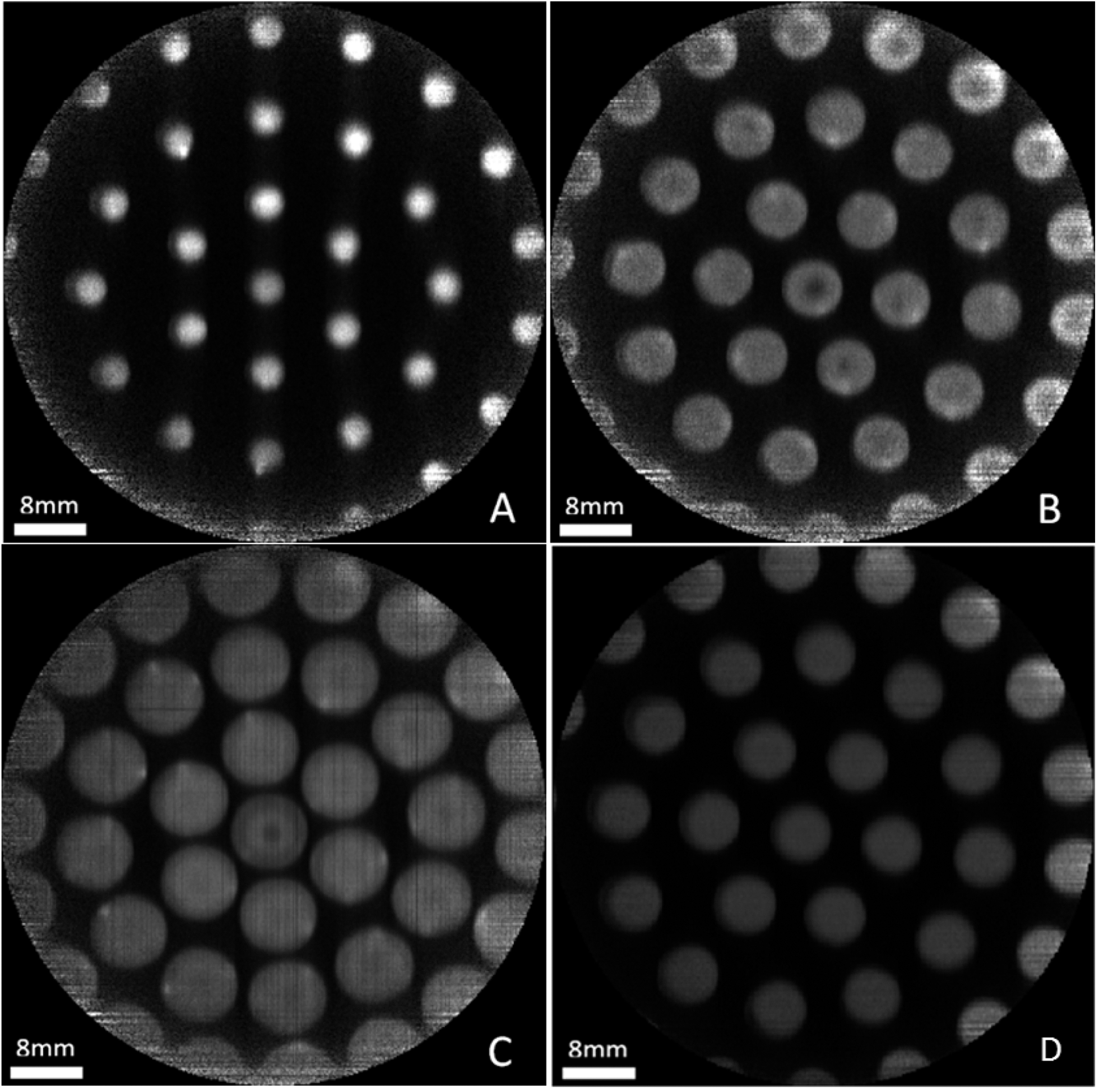
The optimization of the RAAMs allowed testing the feasibility of this approach for GDOES elemental mapping. Thus, a heterogeneous model sample was prepared with a copper substrate by inserting 1 mm silver inclusions separated by 1 mm in the form of a cross to coincide with the apertures. GDOES elemental map with 6 mm i.d. RAAM were obtained at 328.1 nm (Fig. 9A, for silver) and 324.7 nm (Fig. 9B, for copper). A clear contrast is visible between the areas made from silver and those from copper, which shows the viability of RAAM GDOES elemental mapping.
 | ||
| Fig. 9 RAAM GDOES elemental mapping images of silver inlay copper substrate with 6 mm aperture i.d., 2130 Pa, 4 watt mm−2, 16 μs pulse duration, 10 μs ICCD gate duration, 6 μs ICCD gate delay at: (A) 328.1 nm showing silver emission and (B) 324.7 nm showing copper emission. | ||
Conclusion
It has been shown that open face glow discharges on large diameter (100 mm) samples are plagued by heterogeneities at higher pressures that make them impractical for elemental mapping. Nevertheless, it has also been demonstrated that these heterogeneities can be overcome by use of restrictive anode array masks, which are perforated conducting plates held parallel to the cathode sample within a distance of less than 200 μm. RAAMs allow for the analysis of large areas using several smaller glow discharges simultaneously, greatly homogenizing the emission intensity throughout the field of view. Based on the data presented, it was found that a RAAM with 6 mm apertures would produce the homogeneous plasma under elemental mapping conditions when operated with a power density of 4 watt mm−2. Future studies will be aimed at fine-tuning the RAAM design in terms of decoupling the aperture i.d. effect from the inter-aperture distance. In addition, different geometries will be studied to find the most efficient way to analyze wider fields of view while maintaining appropriate power densities and plasma homogeneity. Finally, applications for analysis of samples of interest will be pursued. The development of RAAMs will allow for the full potential of GDOES elemental mapping to be harnessed in terms of ultra-high throughput chemical imaging of large-diameter samples.Acknowledgements
The authors would like to acknowledge financial support from the Texas Tech University Center of Active Learning and Undergraduate Engagement as well as the Texas Tech University Center for the Integration of STEM Education and Research. Scott Hiemstra of the Texas Tech University Department of Chemistry and Biochemistry Machine shop is also gratefully acknowledged for the construction of the glow discharge chamber as well as the Restrictive Anode Array Masks.References
- G. Gamez, S. J. Ray, F. J. Andrade, M. R. Webb and G. M. Hieftje, Anal. Chem., 2007, 79, 1317–1326 CrossRef CAS.
- G. Gamez, M. Voronov, S. J. Ray, V. Hoffmann, G. M. Hieftje and J. Michler, Spectrochim. Acta, Part B, 2012, 70, 1–9 CrossRef CAS PubMed.
- V. Hoffmann, R. Dorka, L. Wilken, V. D. Hodoroaba and K. Wetzig, Surf. Interface Anal., 2003, 35, 575–582 CrossRef CAS.
- M. R. Webb, V. Hoffmann and G. M. Hieftje, Spectrochim. Acta, Part B, 2006, 61, 1279–1284 CrossRef PubMed.
- R. Payling, D. G. Jones and A. Bengtson, Glow discharge optical emission spectrometry, J. Wiley, New York Chichester, 1997 Search PubMed.
- K. R. Marcus and J. A. C. Broekaert, Glow Discharge Plasmas in Analytical Spectroscopy, John Wiley & Sons, New York, 2003 Search PubMed.
- P. Sánchez, B. Fernández, A. Menéndez, R. Pereiro and A. Sanz-Medel, J. Anal. At. Spectrom., 2010, 25, 370–377 RSC.
- T. Nelis, R. Payling and Royal Society of Chemistry (Great Britain), Glow discharge optical emission spectroscopy: a practical guide, Royal Society of Chemistry, Cambridge, UK, 2003 Search PubMed.
- M. R. Winchester and R. Payling, Spectrochim. Acta, Part B, 2004, 59, 607–666 CrossRef PubMed.
- G. Gamez, D. Frey and J. Michler, J. Anal. At. Spectrom., 2012, 27, 50–55 RSC.
- G. Gamez, G. Mohanty and J. Michler, J. Anal. At. Spectrom., 2013, 28, 1016–1023 RSC.
- G. Gamez, G. Mohanty and J. Michler, J. Anal. At. Spectrom., 2014, 29, 315–323 RSC.
- C. Gonzalez de Vega, D. Alberts, V. Chawla, G. Mohanty, I. Utke, J. Michler, R. Pereiro, N. Bordel and G. Gamez, Anal. Bioanal. Chem., 2014, 406, 7533–7538 CrossRef CAS PubMed.
- M. R. Winchester and M. L. Salit, Spectrochim. Acta, Part B, 1995, 50, 1045–1058 CrossRef.
- V. Hoffmann and G. Ehrlich, Spectrochim. Acta, Part B, 1995, 50, 607–616 CrossRef.
- W. F. Maier, K. Stowe and S. Sieg, Angew. Chem., Int. Ed., 2007, 46, 6016–6067 CrossRef CAS PubMed.
- J. S. Garcia, C. S. de Magalhães and M. A. Z. Arruda, Talanta, 2006, 69, 1–15 CrossRef CAS.
- S. Rahimi, L. Tao, S. F. Chowdhury, S. Park, A. Jouvray, S. Buttress, N. Rupesinghe, K. Teo and D. Akinwande, ACS Nano, 2014, 8, 10471–10479 CrossRef CAS PubMed.
- B. A. Sabol, B. Atwood, J. M. Hill, J. T. Williams, M. P. Lesser, P. L. Byard and W. B. Davison, Proc. SPIE1236, Adv. Technol. Optical Telescopes IV, 1990, 940 Search PubMed.
- M. W. Schneermann, M. Groessl, U. Nienaber, E. Ettlinger, J. A. Spiteri and H. Clow, Proc. SPIE2871, Opt. Telescop. of Today and Tomorrow, 1997, 136 Search PubMed.
- M. Voronov, V. Hoffmann, T. Wallendorf, S. Marke, J. Mönch, C. Engelhard, W. Buscher, S. J. Ray and G. M. Hieftje, J. Anal. At. Spectrom., 2012, 27, 419–425 RSC.
- M. Voronov, V. Hoffmann, T. Steingrobe, W. Buscher, C. Engelhard, A. P. Storey, S. J. Ray and G. M. Hieftje, Plasma Sources Sci. Technol., 2014, 23, 054009 CrossRef.
Footnote |
| † Electronic supplementary information (ESI) available. See DOI: 10.1039/c5ja00288e |
| This journal is © The Royal Society of Chemistry 2016 |