 Open Access Article
In situ video-STM studies of the mechanisms and dynamics of electrochemical bismuth nanostructure formation on Au†
H.
Matsushima‡
a,
S.-W.
Lin
b,
S.
Morin
b and
O. M.
Magnussen
*a
aChristian-Albrechts-Universität zu Kiel, Olshausenstr. 40, D-24098 Kiel, Germany. E-mail: magnussen@physik.uni-kiel.de
bYork University, 4700 Keele Street, Toronto, Canada
First published on 16th September 2016
Abstract
The microscopic mechanisms of Bi electrodeposition on Au(111) and Au(100) electrodes in the overpotential regime were studied by in situ scanning tunneling microscopy with high spatial and temporal resolution. Atomic resolution images of the needle-like Bi(110) deposits formed on Au(111) reveal the central influence of covalent Bi–Bi bonds on the deposit morphology. In the straight steps along the needle edges the Bi atoms are interlinked by these bonds, whereas at the needle tip and at kinks along the needle edges dangling bonds exist, explaining the rapid structural fluctuations at these sites. For ultrathin Bi deposits on Au(100) a more open atomic arrangement was found within the surface plane, which was tentatively assigned to an epitaxially stabilised Bi(111) film. Furthermore, well-defined nanowires, consisting of zigzag chains of Bi surface atoms, were observed on this surface.
Introduction
Quasi one-dimensional nanostructures, such as nanowires, nanotubes and nanoribbons, have unique physical and chemical properties and are of substantial interest for nano-electronics and sensor applications.1 Electrodeposition has established itself as a popular technique for the formation of such nanostructures.2 On the one hand, nanowire growth can be achieved by templates, for example by electrodeposition into porous membranes3–5 or by heterogeneous nucleation and growth at one-dimensional defects, such as steps.6–9 On the other hand, intrinsic anisotropies and kinetic effects can result in the spontaneous formation of one-dimensional nanostructures. The latter includes the well-known electrochemical growth of whiskers and dendrites10 as well as the lateral epitaxial growth of nanowires and strongly anisotropic crystallites on electrode surfaces.11–15 Here we investigate the microscopic growth mechanisms of such structures and the atomic-scale growth dynamics for the case of electrodeposited bismuth on Au electrodes.Bi thin films and nanostructures have been receiving much attention in recent years owning to the unusual surface electronic structure of Bi.16,17 Bi exhibits strong spin–orbit coupling, making it of great interest to the field of topological insulators, and has electronic surface states that cross the Fermi level. Phenomena such as surface superconductivity, enhanced thermopower, and high electronic mobility have been observed, which are still under debate. As a consequence the behaviour of Bi nanowires and nanoribbons also strongly deviates from that of the bulk material and changes as a function of the nanostructure diameter and type.18–22 Furthermore, thin Bi films for potential applications in magnetic sensors,23,24 thermoelectric materials17,25 and spin filters26,27 depend strongly on the integrity of the microstructure.28 Bi thin films prepared by electrochemical deposition have been studied in recent years because of this method's ability to provide a better control of the thin film's microstructure, simple processing, such as room temperature operation at atmospheric pressure, and low costs. Electrochemical growth of crystalline Bi thin films has been demonstrated on Au(111)13,29 and GaAs(111),30 resulting in surface morphologies with needle-like and pyramidal islands, respectively. These deposits can be converted into highly ordered single-crystal Bi films by annealing. Similar needle-like morphologies were also found for Bi deposition from the gas phase on Ag(111),31 Si(111)32,33 and graphite.34,35
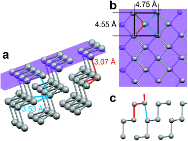
Detailed studies of the initial stage of Bi electrodeposition on Au(111) and Au(100) substrates were performed using in situ STM and in situ surface X-ray scattering measurements.13,36–41 Most of these studies focused on Bi underpotential deposition (UPD), revealing a similar sequence of Bi monolayer phases on both surfaces. With decreasing potential first commensurate Bi superstructures were found, followed by uniaxially-incommensurate quasi-hexagonal adlayers with high packing density. As shown by X-ray diffraction studies, bulk Bi deposition on Au(111) occurs in the form of an epitaxial film, in which the Bi(110) plane§ is oriented parallel to the Au surface (see Fig. 1).29 An in situ STM study of the Bi growth behaviour was reported by Jeffrey et al.13 At low overpotential (≈−0.08 VSCE) the growth of these films was found to start with the formation of an isotropic Bi bilayer on the terraces, followed by the formation of nuclei at step edges and defect sites. These nuclei develop into highly anisotropic needle-like structures which are oriented with the long axis parallel to the Au surface and which grow quite rapidly. This needle growth mode is observed up to many hundreds of layers, resulting in a Bi film of increasing roughness. However, a clear mechanism of the nucleation and growth of these needles is still lacking, because of the high growth rate and the resulting difficulties in following this process using a conventional in situ STM.
Such atomic-scale studies of fast dynamic processes at electrochemical interfaces have become feasible using in situ video STM, performed in constant height mode at scan rates of 10 to 30 images per second.42 In particular, video STM has been employed in the past for studies of electrochemical crystal growth and dissolution processes43–45 and of the dynamics of quasi one-dimensional nanostructures on electrode surfaces.46–49 Bi deposition on Au single crystal electrodes in HClO4 solution is well suited for such video STM studies because (i) the ClO4− anions are not specifically adsorbed on Bi and hence do not affect the Bi growth and (ii) the Bi electrodeposit exhibits a well-defined crystalline structure with extended terraces. In this paper we describe the structure and dynamics of Bi growth on Au(111) and Au(100). We especially focus on the origin of the pronounced anisotropy in this deposition process, manifesting in the formation of Bi needles and nanowires. The dynamic behaviour of kinks along the Bi needle edges is analysed quantitatively and interpreted taking the Bi lattice structure into account.
Experimental
The study was performed using the home-built in situ electrochemical video STM of the Kiel group.42 All images presented in this work were recorded at a rate of 10–20 images per second in constant height mode. STM tips were etched from W-wire and coated with ethylene–vinyl acetate polymer, leaving the very end exposed. The tip and sample were independently kept under potentiostatic control.The electrochemical cell consisted of a Kel-f cell with a charged palladium hydride electrode (Pd–H) as a reference, a Pt wire as a counter electrode and a Au(111) or Au(100) single crystal (orientation ≤ ±0.5°, Monocrystal Co.) as a working electrode. The Pd–H electrode was charged prior to the experiment in a dilute sulfuric acid solution and exhibited a stable potential (ca. −0.20 V, vs. SCE) in the bismuth containing electrolytes. All the cell potentials reported in this work are given with respect to the saturated calomel electrode (SCE). The Au crystal was cleaned in suprapure sulfuric acid and rinsed in ultrapure water (Elga Lab water, 18.2 MΩ resistance). The crystal was then flame annealed for several minutes and cooled down in air before being mounted in the video STM cell. The Bi electrolytes, containing 0.5 or 1 mM Bi3+, were prepared by dissolving Bi2O3 (Alfa Aesar, 99.9995%) in 0.1 M HClO4 (ultrapure grade, Seastar Chemicals Inc.) prepared using ultrapure water. In all experiments, the initial potential was chosen between 0.05 and −0.08 V, i.e. at a value more positive than the corresponding Bi3+/Bi Nernst potential, to avoid Bi bulk deposition. Subsequently, the potential was stepped down to more negative values in the overpotential deposition (OPD) regime to investigate the growth of bulk Bi.
Results and discussion
Bismuth growth on Au(111)
In situ video STM experiments performed on Au(111) electrodes in the Bi OPD potential regime reveal the same needle growth behaviour observed using the conventional STM. When the cell potential is stepped to higher overpotentials (<−0.10 V), rapid formation of Bi multilayer deposits commences. Because the surface roughness in this stage of the growth process is initially high, the (constant-height mode) video-rate imaging is impeded and high-resolution images of the deposit cannot be obtained. However, 1 to 2 minutes after the onset of Bi bulk deposition the growth rate slows down and the characteristic Bi needle structure can be observed with atomic resolution (Fig. 2a). The Bi surface lattice is described by a pseudo-square structure with a prominent maximum at the corners of the unit cell and a weaker maximum slightly of center (shifted to the left of the unit cell center in the image in Fig. 2a). This structure is in full agreement with the arrangement of Bi atoms in the Bi(110) plane (Fig. 1b). Within this plane parallel running zigzag chains of covalently bound Bi atoms are located. Each surface atom thus exhibits two covalent bonds of 3.07 Å length (indicated in red) to atoms within the chain and two longer non-covalent bonds with 3.53 Å bonding distance (indicated in blue) to atoms in the neighbouring chain. Very similar UHV-STM images were obtained on needle-like Bi deposits on Ag(111) and assigned to an identical structure.31 In some in situ video STM images obtained at larger bias only one of the atoms in the pseudo-square unit cell was resolved. Those observations strongly resemble high-resolution in situ STM images obtained in the previous study of Bi on Au(111) by Jeffrey et al.13 as well as in UHV-STM experiments of Bi(110) films on Si(111)-(7 × 7).32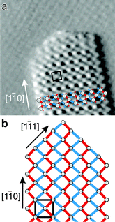 | ||
| Fig. 2 (a) High-resolution in situ video STM image of the needle-like Bi deposit structure obtained on Au(111) at −0.19 V (46 × 46 Å2). (b) Schematic model of the atomic structure of the Bi needles. | ||
The characteristic needle-like growth morphology can be clearly correlated with the anisotropic atomic structure of the Bi deposit. The Bi needles are oriented perfectly parallel to the [1![[1 with combining macron]](https://www.rsc.org/images/entities/char_0031_0304.gif) 0] direction of the Bi lattice, i.e. along the direction of the covalently bound chains. Apart from a few kinks during needle growth and dissolution (see below), the needle edges along this direction are perfectly straight. Interestingly, each needle consists of an odd number of Bi rows, i.e. the needles are (n + 1/2) unit cells wide (with n being a natural number). As illustrated schematically in Fig. 2b, these observations can be rationalised by an atomic arrangement where the needles are on both edges terminated by Bi chains. In this type of structure all Bi atoms at the needle edges are energetically stabilized by two covalent bonds to neighbouring edge atoms.
0] direction of the Bi lattice, i.e. along the direction of the covalently bound chains. Apart from a few kinks during needle growth and dissolution (see below), the needle edges along this direction are perfectly straight. Interestingly, each needle consists of an odd number of Bi rows, i.e. the needles are (n + 1/2) unit cells wide (with n being a natural number). As illustrated schematically in Fig. 2b, these observations can be rationalised by an atomic arrangement where the needles are on both edges terminated by Bi chains. In this type of structure all Bi atoms at the needle edges are energetically stabilized by two covalent bonds to neighbouring edge atoms.
The needle-like Bi islands shown as examples in Fig. 2a grow on top of a smooth Bi(110) terrace (the pseudo-square unit cell of the latter surface is only faintly visible due to the much higher tunnelling distance in these constant height images). They are of monolayer height, which is in contrast to the needle-like Bi islands observed in UHV-STM studies of gas phase deposited Bi films.31–35 In the latter case the step heights typically corresponded to multiples of bilayers. This was attributed to a bilayer arrangement as in black phosphorous, where the out-of-plane dangling bonds of the Bi atoms pair up. Depending on the substrate the planes in the black phosphorous structure were found to be either flat or buckled. Our experimental observations suggest a bulk like (110) structure of the Bi deposit on Au(111) electrodes rather than a flat or buckled black phosphorous phase: first, no preference for films with an even number of Bi layers is found. Second, the two atoms in the Bi(110) surface unit cell appear significantly different in the STM images whereas no such difference in contrast was observed in high-resolution UHV-STM studies.31,32,34,50 For a bulk-like (110) film the two atoms in the unit cell are chemically non-equivalent, which could explain this difference in contrast. Specifically, the atoms in the center of the unit cell of Fig. 1b exhibit dangling bonds towards the electrolyte while those in the unit cell corners would have covalent bonds to the underlying Bi layer. This structural difference of the Bi(110) film in our study and under vacuum conditions may be caused by the termination of the dangling bonds by adsorbed species from the electrolyte. In view of the negative deposition potential the most likely candidate is adsorbed hydrogen, which readily binds to these sites.32,51–53 Evidence for the adsorption of hydrogen species, especially on Bi surfaces exhibiting covalent bonds, was also obtained in studies of hydrogen evolution.54 In contrast, the presence of other species, such as adsorbed anions or OH, can be ruled out in this potential regime.55
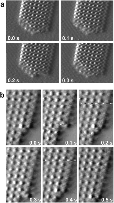
The dynamics of the Bi islands reflects their anisotropic structure. While the long, atomically smooth steps along the [1![[1 with combining macron]](https://www.rsc.org/images/entities/char_0031_0304.gif) 0] direction are very stable, the tips of the needle-like islands exhibit rough and highly mobile steps. In atomic resolution in situ video STM measurements these tips often appear blurry and change from image to image (see Fig. 3a and video 1 in the ESI†), indicating fast attachment and detachment of Bi adatoms. This instability of the step edge atoms at the needle tips can be explained within the structural model proposed above. Because the zigzag chains are terminated at the tips, these atoms have a lower number of covalent bonds to neighbouring Bi atoms than the atoms at the [1
0] direction are very stable, the tips of the needle-like islands exhibit rough and highly mobile steps. In atomic resolution in situ video STM measurements these tips often appear blurry and change from image to image (see Fig. 3a and video 1 in the ESI†), indicating fast attachment and detachment of Bi adatoms. This instability of the step edge atoms at the needle tips can be explained within the structural model proposed above. Because the zigzag chains are terminated at the tips, these atoms have a lower number of covalent bonds to neighbouring Bi atoms than the atoms at the [1![[1 with combining macron]](https://www.rsc.org/images/entities/char_0031_0304.gif) 0] oriented steps (see Fig. 2b). The weak tendency of the steps at the needle tips to orient roughly along the [1
0] oriented steps (see Fig. 2b). The weak tendency of the steps at the needle tips to orient roughly along the [1![[1 with combining macron]](https://www.rsc.org/images/entities/char_0031_0304.gif) 1] orientation suggests that the step edge atoms can also be partly stabilized by the non-covalent bonds; however, this effect is much less pronounced than that of the covalent coordination.
1] orientation suggests that the step edge atoms can also be partly stabilized by the non-covalent bonds; however, this effect is much less pronounced than that of the covalent coordination.
The same tendencies manifest in video STM studies of the motion of kinks along the straight [1![[1 with combining macron]](https://www.rsc.org/images/entities/char_0031_0304.gif) 0] oriented steps. These studies reveal that the kink motion proceeds via the addition or removal of two rows of Bi atoms in a zigzag fashion, i.e. via one-dimensional growth or dissolution of a chain of covalently bound Bi surface atoms along the island edge (see Fig. 3b and video 2†). Three types of kinks were observed in the STM videos, which are illustrated in Fig. 4: typically, kinks are of the type denominated as A or B in Fig. 4 and propagate along the step edge by alternating between these two states. Examples of these types of kinks can be observed e.g. in Fig. 3b. In more rare cases steps of the type C are observed in the images. Also in this case kink propagation occurs via subsequent changes between the type C and the type B state.
0] oriented steps. These studies reveal that the kink motion proceeds via the addition or removal of two rows of Bi atoms in a zigzag fashion, i.e. via one-dimensional growth or dissolution of a chain of covalently bound Bi surface atoms along the island edge (see Fig. 3b and video 2†). Three types of kinks were observed in the STM videos, which are illustrated in Fig. 4: typically, kinks are of the type denominated as A or B in Fig. 4 and propagate along the step edge by alternating between these two states. Examples of these types of kinks can be observed e.g. in Fig. 3b. In more rare cases steps of the type C are observed in the images. Also in this case kink propagation occurs via subsequent changes between the type C and the type B state.
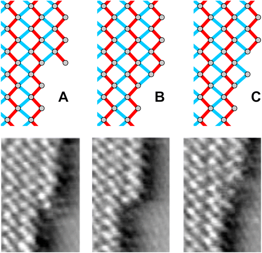 | ||
| Fig. 4 Different types of kinks observed along the edges of Bi needles on Au(111) and corresponding examples, taken from an STM video. | ||
The microscopic growth rates found in these experiments are much lower than those which would be expected at the rather high overpotentials employed. We attribute this to geometric shielding by the STM tip, which is a well-known effect in in situ STM studies of electrodeposition processes.56 Nevertheless, the video STM observations of the structural fluctuations at the kinks provide interesting additional information on the Bi deposits. Because these fluctuations occur on the hundred millisecond time scale, the different kink configurations can be sampled with good statistics. According to our data, the different types of kinks are observed with very different probabilities. Based on an analysis of 750 kinks, we find the type B kinks with 81% probability, type A kinks with 16% probability and type C kinks with only 3% probability. Within the experimental errors no clear dependence on potential was found in the range −0.10 to −0.64 V. These statistical data reflect the different probabilities pj (j = A, B, C) for a kink to be in one of the three observed states, i.e. the different residence times of the kinks to be in one of these configurations. Because the studies were performed at low kink propagation rates and thus are close to equilibrium, these statistical data allow the calculation of the relative energy difference ΔEij between these kinks via the Boltzmann equation ΔEij = −kBT![[thin space (1/6-em)]](https://www.rsc.org/images/entities/char_2009.gif) ln(pi/pj). Using the statistical data obtained in the video STM measurements (performed at T = 298 K) one obtains an increase in energy of ΔEAB = 42 ± 3 meV of the type A and of ΔECB = 86 ± 7 meV of the type C kinks as compared to the type B kinks, respectively.
ln(pi/pj). Using the statistical data obtained in the video STM measurements (performed at T = 298 K) one obtains an increase in energy of ΔEAB = 42 ± 3 meV of the type A and of ΔECB = 86 ± 7 meV of the type C kinks as compared to the type B kinks, respectively.
We interpret these results in terms of the different coordination of the Bi atoms at the kink in the three different states. In the type A kinks the Bi atoms at the kink are missing two non-covalent bonds to neighbouring atoms as compared to the type B kinks; type C kinks are even lacking two covalent bonds. Taken this into account, the energy differences at a first glance seem smaller than expected from the Bi cohesive energy (2.16 eV per atom57) or the Bi–Bi bond energy (2.08 eV (ref. 58)). However, the energy balance may be strongly affected by the presence of coadsorbates. Recent density functional theory calculations for two-dimensional Bi nanoribbons with similar covalently bound Bi chains along the edges found strong modification of the geometric and electronic structure by hydrogen adsorption at the dangling bonds of the terminating Bi atoms.51–53 Hydrogen adsorption energies in the range of 2.2 eV were reported.52 Similar behaviour may be expected in the electrochemical environment and may significantly reduce the kink energies.
Bismuth growth on Au(100)
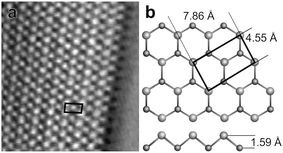
Similar in situ video STM studies of Bi electrodeposition were performed on Au(100) electrodes. In contrast to the structure of the Bi UPD adlayer on Au(100), which has been characterized in detail by STM and X-ray surface diffraction,36,40 the initial stages of Bi bulk electrodeposition have not been reported before. High-resolution video STM images recorded in the overpotential range (Fig. 5a) find a lattice structure that clearly differs from that of the UPD layer or of the Bi(110) film observed on Au(111). In particular, these Bi deposits exhibit a much more open atomic structure, which is incompatible with Bi(110) or the c(p × 2) Bi UPD layer. The observed surface structure is described by a rectangular unit cell with one prominent and one weaker maximum that form alternating rows. Upon assigning both of these to Bi surface atoms, a (pseudo-) hexagonal arrangement results. The interatomic distances are in good agreement with those in an atomic layer of the (111) plane of bulk Bi (shown in the model in Fig. 5b). In this plane the Bi atoms form hexagonally ordered bilayers, interlinked by covalent bonds. This assignment assumes that only the topmost Bi(111) layer is visible in the STM images, which is likely in view of the 1.59 Å spacing to the underlying second layer (see Fig. 5b, bottom).Bi(111) is the natural cleavage plane of bismuth and under UHV conditions the preferred orientation in epitaxial growth.16 The surface atoms in Bi(111) have a lower number of non-covalent long bonds to neighbouring atoms as compared to those in the Bi(110) surface, but – in contrast to the latter – do not exhibit dangling bonds. For thick epitaxial Bi films formed by electrodeposition on Au(100) a (110) orientation has been found.59 However, Bi(110) and Bi(111) films are similar in energy and structural transitions between them have been found in ultrathin epitaxial films.32,60 It therefore seems possible that a Bi(111) structure is epitaxially stabilized in the very thin films studied in this work (typically consisting of only a few layers).
Although a Bi(111) film would account for the observed inter-atomic spacings of the surface atoms, it cannot explain the row-like modulation of the structure. The latter would not be expected for true Bi(111) films and was not observed in previous STM studies of (111) oriented Bi films on Si(111).32,60 Most likely, these rows result from epitaxy to the underlying Au substrate lattice. This is supported by observations of the deposit morphology on larger length scales, which show that the rows in different Bi islands are arranged at well-defined angles of 90° with respect to each other (see below). Interestingly, the 7.86 Å spacing between next-nearest neighbour atoms of the topmost Bi(111) layer differs by only 3.7% from 2aAu (with aAu = 4.08 Å being the Au lattice constant). Furthermore, the Bi spacing in the perpendicular direction is only 11.5% larger than aAu. Minor deformation of the Bi(111) bilayer lattice thus allows it to transform into a structure that is fully commensurate by the Au(100) lattice and can be described by a (√2 × 2√2)R45° superstructure. In this structure half of the second layer Bi atoms would occupy the energetically preferred fourfold-hollow sites while the remaining half would reside on top sites, explaining the vertical modulation. The length of the covalent Bi–Bi bonds can be preserved in this arrangement by a small vertical relaxation of the bilayer distance; the bond angles likewise will only be slightly distorted. Such a commensurate structure may significantly reduce the Bi–Au interface energy and by this stabilize ultrathin Bi(111) films. For thicker deposits the epitaxial stress associated with this structure should drive a structural transition, apparently resulting in a Bi(110) film.
Observations of the growth morphology and dynamics support that the ultrathin Bi deposits on Au(100) differ structurally from the Bi(110) film found on Au(111). First, the observed Bi islands are rectangular in shape rather than needle-like. Similar to the latter they exhibit relatively straight edges which are preferentially oriented along the direction of the atomic rows. Typically, the islands are terminated by one of the rows that appear to be of lower apparent height in the STM images (see Fig. 5a). However, compared to the Bi deposits on Au(111) these steps usually exhibit a much larger number of kinks that often are multiple rows wide.
The typical structure and dynamic behaviour of these kinks is illustrated in Fig. 6. Kinks in the step are usually one unit cell (or a multiple thereof) wide, i.e. consisting of two Bi rows. They are predominantly terminated by an atomically smooth edge (see e.g.Fig. 6, 0.0 s) or an additional atom in the kink corner (Fig. 6, 0.1 s), resembling the B and C type kinks illustrated in Fig. 4. However, the kinks propagate in a much more irregular fashion along the step edges than for Bi on Au(111). In particular, single rows that extend several atoms away from the kink are often formed transiently during island growth or dissolution (Fig. 6, 0.2–0.3 s). Such structures were never observed in videos of kink propagation along the edges of the needle-like Bi(110) islands, where they would correspond to atoms that are bound to the step only by long non-covalent bonds (see model of C type kinks in Fig. 4) and thus are energetically very unfavourable. In contrast, these observations can be easily reconciled with a Bi(111) deposit. Because all covalent bonds of the Bi surface atoms in the (111) plane are to atoms in the underlying second layer, the different kink configurations should be similar in energy. A difference between the high and the low atomic rows could in this case only come from the different epitaxial relationship with respect to the substrate lattice, which should be a more minor effect.
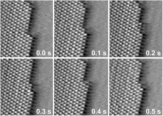 | ||
| Fig. 6 Sequences of STM images of Bi deposits on Au(100), taken from a video recorded at 10 Hz and a potential of −0.17 V. The images show kink propagation along the island edge (75 × 70 Å2). | ||
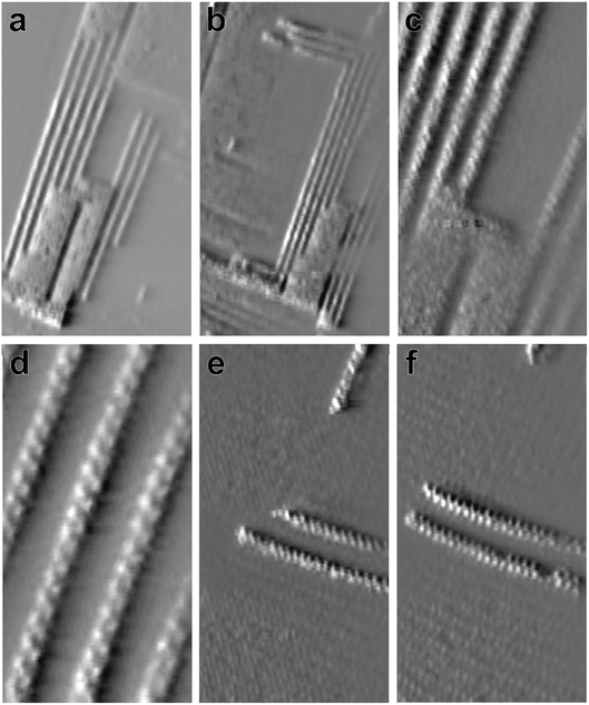
In addition to these two-dimensional islands spontaneous formation of truly one-dimensional nanowires was observed for Bi deposition on the Au(100) surface (Fig. 7). These nano-wires are of well-defined width and can be several tens of nanometers long. They grow predominantly away from the edges of the Bi islands, following the directions of the atomic rows (see Fig. 7c). Furthermore, structural fluctuations are observed in which Bi islands are converted into nanowires and vice versa. Often the nanowires form arrays with well-defined spacings that are exactly five times the distance between the atomic rows in the Bi islands (Fig. 7a–d). In more rare cases freestanding nanowires are also observed (Fig. 7e and f). The nanowires slowly grow with time, both in length and number, as can be seen in the image in Fig. 7b, recorded 25.5 s after the image in Fig. 7a in the same surface area. In addition, rapid fluctuations are found, especially for isolated free-standing nanowires. However, these fluctuations may be (at least partly) induced by the STM tip.
High-resolution images of the nanowires (Fig. 7d–f) reveal that they consist of a zigzag chain of atoms. As visible in the images in which the underlying Bi film is atomically resolved (Fig. 7e and f), these chains are commensurate to the Bi lattice. That is, the nanowires are exactly one of the rectangular unit cells of the Bi film wide and are oriented in the direction of the shorter unit cell vector. In areas where the nanowires are 90° rotated (e.g. in the upper right corner of Fig. 7e and f) the atomic rows in the underlying Bi substrate also run in the perpendicular direction. These observations indicate that the nanowires grow epitaxially on the Bi bulk deposit and, most likely, are structurally related to the latter. However, it is currently unclear what stabilises the unique one-dimensional morphology of these structures.
Conclusions
As demonstrated by these in situ video STM studies, Bi electrodeposition exhibits a rich microscopic growth behaviour, reflecting its unique material properties. A central aspect governing the deposit morphology and dynamic is the presence of short bonds with pronounced covalent character. These bonds have already been found to determine the epitaxial growth of ultrathin Bi films under UHV conditions as well as to strongly influence the electronic surface and edge states of one-dimensional Bi nanostructures – a topic of great current interest. Our observations indicate that the presence of covalent Bi–Bi bonds also governs epitaxial growth in an electrochemical environment. Specifically, the formation of the needle-like Bi deposits on Au(111) found in previous STM studies can be clearly rationalised by the structural anisotropy in the deposit caused by these bonds. The latter interlink the atoms in the Bi(110) surface in the form of one-dimensional chains that define the needle direction. Growth and dynamic fluctuations occur predominantly at the end of these chains.While thick Bi electrodeposits grow in the form of a Bi(110) film on Au(111) as well as on Au(100), video STM investigations of ultrathin deposits reveal a very different structure and growth morphology. As indicated by these data, the structure of ultrathin Bi electrodeposits may be strongly affected by epitaxial effects. On the basis of our structural observations we suggested the formation of a Bi(111) like film on Au(100), which is commensurate to the square substrate lattice. Independent confirmation of this deposit structure, e.g. by surface X-ray diffraction studies, would be highly desirable. Particularly interesting is the surprising observation of truly one-dimensional Bi nanowires on this surface. Structures of this type have not been reported in previous studies of Bi deposits, including deposits formed under vacuum conditions. Although their origin is currently unclear, they represent unique nanostructures with potentially interesting novel properties. In particular, one-dimensional Bi nanostructures are of great current interest in the field of topological insulators. The epitaxial electrodeposition of Bi may thus offer attractive new possibilities for the formation of such structures.
Acknowledgements
We gratefully acknowledge financial support by the Deutsche Forschungsgemeinschaft via MA 1618/11 and MA 1618/15, NSERC for a Discovery Grant and a Canada Research Chair (S. M.), a fellowship for S. M. by the Alexander von Humboldt-Stiftung, and field trip funds from York University for S.-H. L.Notes and references
- Y. Xia, P. Yang, Y. Sun, Y. Wu, B. Mayers, B. Gates, Y. Yin, F. Kim and H. Yan, Adv. Mater., 2003, 15, 353 CrossRef CAS.
- G. Staikov, in Electrocrystallization in nanotechnology, Wiley-VCH, Weinheim, 2007 Search PubMed.
- T. R. Kline, M. Tian, J. Wang, A. Sen, M. W. H. Chan and T. E. Mallouk, Inorg. Chem., 2006, 45, 7555 CrossRef CAS PubMed.
- H. Schloerb, V. Haehnel, M. S. Khatri, A. Srivastav, A. Kumar, L. Schultz and S. Faehler, Phys. Status Solidi B, 2010, 247, 2364 CrossRef CAS.
- U. S. Mohanty, J. Appl. Electrochem., 2011, 41, 257 CrossRef CAS.
- R. M. Penner, J. Phys. Chem. B, 2002, 106, 3339 CrossRef CAS.
- R. M. Penner, Mod. Aspects Electrochem., 2009, 45, 175 CAS.
- S. Morin, A. Lachenwitzer, O. M. Magnussen and R. J. Behm, Phys. Rev. Lett., 1999, 83, 5066 CrossRef CAS.
- X. Xiao, M. Nielinger and H. Baltruschat, Electrochim. Acta, 2003, 48, 3093 CrossRef CAS.
- J. K. Chang, C. M. Wu and I. W. Sun, J. Mater. Chem., 2010, 20, 3729 RSC.
- F. Möller, O. M. Magnussen and R. J. Behm, Phys. Rev. Lett., 1996, 77, 3165 CrossRef PubMed.
- S. Strbac, O. M. Magnussen and R. J. Behm, Phys. Rev. Lett., 1999, 83, 3246 CrossRef CAS.
- C. A. Jeffrey, D. A. Harrington and S. Morin, Surf. Sci., 2002, 512, L367 CrossRef CAS.
- S. Takakusagi, K. Kitamura and K. Uosaki, J. Phys. Chem. C, 2008, 112, 3073 CAS.
- R. Wen, G. B. Pan and L. J. Wan, J. Am. Chem. Soc., 2008, 130, 12123 CrossRef CAS PubMed.
- P. Hofmann, Prog. Surf. Sci., 2006, 81, 191 CrossRef CAS.
- T. E. Huber, K. Owusu, S. Johnson, A. Nikolaeva, L. Konopko, R. C. Johnson and M. J. Graf, J. Appl. Phys., 2012, 111, 043709 CrossRef.
- L. Li, Y. Yang, X. Fang, M. Kong, G. Li and L. Zhang, Solid State Commun., 2007, 141, 492 CrossRef CAS.
- M. Tian, J. Wang, Q. Zhang, N. Kumar, T. E. Mallouk and M. H. W. Chan, Nano Lett., 2009, 9, 3196 CrossRef CAS PubMed.
- K. Lee, S. Lee, S. N. Holmes, J. Ham, W. Lee and C. H. W. Barnes, Phys. Rev. B: Condens. Matter Mater. Phys., 2010, 82, 245310 CrossRef.
- J. Kim, S. Lee, Y. M. Brovman, M. G. Kim, P. Kim and W. Lee, Appl. Phys. Lett., 2014, 104, 043105 CrossRef.
- M. Tian, J. Wang, W. Ning, T. E. Mallouk and M. H. W. Chan, Nano Lett., 2015, 15, 1487 CrossRef CAS PubMed.
- F. Y. Yang, K. Liu, K. M. Hong, D. H. Reich, P. C. Searson and C. L. Chien, Science, 1999, 284, 1335 CrossRef CAS PubMed.
- F. Y. Yang, K. Liu, C. L. Chien and P. C. Searson, Phys. Rev. Lett., 1999, 82, 3328 CrossRef CAS.
- Z. Zhang, X. Sun, M. S. Dresselhaus, J. Y. Ying and J. Heremans, Phys. Rev. B: Condens. Matter Mater. Phys., 2000, 61, 4850 CrossRef CAS.
- Y. Koroteev, G. Bihlmayer, J. E. Gayone, E. V. Chulkov, S. Blügel, P. M. Echenique and P. Hofmann, Phys. Rev. Lett., 2004, 93, 046403 CrossRef PubMed.
- T. Hirahara, T. Nagao, I. Matsuda, G. Bihlmayer, E. V. Chulkov, Y. Koroteev, P. M. Echenique, M. Saito and S. Hasegawa, Phys. Rev. Lett., 2006, 97, 146803 CrossRef CAS PubMed.
- B. O'Brien, M. Plaza, L. Y. Zhu, L. Perez, C. L. Chien and P. C. Searson, J. Phys. Chem. C, 2008, 112, 12018 Search PubMed.
- C. A. Jeffrey, S. H. Zheng, E. Bohannan, D. A. Harrington and S. Morin, Surf. Sci., 2005, 600, 95 CrossRef.
- Z. L. Bao and K. L. Kavanagh, Appl. Phys. Lett., 2006, 88, 063708 Search PubMed.
- H. L. Zhang, W. Chen, X. S. Wang, J. Yuhara and A. T. S. Wee, Appl. Surf. Sci., 2009, 256, 460 CrossRef CAS.
- T. Nagao, J. T. Sadowski, M. Saito, S. Yaginuma, Y. Fujikawa, T. Kogure, T. Ohno, Y. Hasegawa, S. Hasegawa and T. Sakurai, Phys. Rev. Lett., 2004, 93, 105501 CrossRef CAS PubMed.
- S. Yaginuma, T. Nagao, J. T. Sadowski, M. Saito, K. Nagaoka, Y. Fujikawa, T. Sakurai and T. Nakayama, Surf. Sci., 2007, 601, 3593 CrossRef CAS.
- P. J. Kowalczyk, O. Mahapatra, D. N. McCarthy, W. Kozlowski, Z. Klusek and S. A. Brown, Surf. Sci., 2011, 605, 659 CrossRef CAS.
- P. J. Kowalczyk, O. Mahapatra, S. A. Brown, G. Bian, X. Wang and T. C. Chiang, Nano Lett., 2013, 13, 43 CrossRef CAS PubMed.
- S. H. Zheng, K. Krug, F. Golks, D. Kaminski, S. Morin and O. M. Magnussen, J. Electroanal. Chem., 2010, 649, 189 CrossRef CAS.
- C.-H. Chen and A. A. Gewirth, J. Am. Chem. Soc., 1992, 114, 5439 CrossRef CAS.
- C. Chen, K. D. Kepler, A. A. Gewirth, B. M. Ocko and J. Wang, J. Phys. Chem., 1993, 97, 7290 CrossRef CAS.
- K. Tamura, B. M. Ocko, J. X. Wang and R. R. Adzic, J. Phys. Chem. B, 2002, 106, 3896 CrossRef CAS.
- M. Hara, Y. Nagahara, S. Yoshimoto, J. Inukai and K. Itaya, J. Electrochem. Soc., 2004, 151, E92 CrossRef CAS.
- M. Nakamura, N. Sato, N. Hoshi and O. Sakata, Langmuir, 2010, 26, 4590 CrossRef CAS PubMed.
- L. Zitzler, B. Gleich, O. M. Magnussen and R. J. Behm, Proceedings of the Electrochemical Society, 2000, vol. 99–28, p. 29 Search PubMed.
- O. M. Magnussen, L. Zitzler, B. Gleich, M. R. Vogt and R. J. Behm, Electrochim. Acta, 2001, 46, 3725 CrossRef CAS.
- O. M. Magnussen, W. Polewska, L. Zitzler and R. J. Behm, Faraday Discuss., 2002, 121, 43 RSC.
- W. Polewska, R. J. Behm and O. M. Magnussen, Electrochim. Acta, 2003, 48, 2915 CrossRef CAS.
- M. Labayen and O. M. Magnussen, Surf. Sci., 2004, 573, 128 CrossRef CAS.
- M. Labayen, C. Haak and O. M. Magnussen, Phys. Rev. B: Condens. Matter Mater. Phys., 2005, 71, 241409–241411 CrossRef.
- H. Matsushima, A. Taranovskyy, C. Haak, Y. Gründer and O. M. Magnussen, J. Am. Chem. Soc., 2009, 131, 10362 CrossRef CAS PubMed.
- H. Matsushima, C. Haak, A. Taranovskyy, Y. Gründer and O. M. Magnussen, Phys. Chem. Chem. Phys., 2010, 12, 13992 RSC.
- Y. Lu, W. Xu, M. Zeng, G. Yao, L. Shen, M. Yang, Z. Luo, F. Pan, K. Wu, T. Das, P. He, J. Jiang, J. Martin, Y. P. Feng, H. Lin and X. S. Wang, Nano Lett., 2015, 15, 80 CrossRef CAS PubMed.
- Z. F. Wang, L. Chen and F. Liu, Nano Lett., 2014, 14, 2879 CrossRef CAS PubMed.
- L. Chen, G. Cui, P. Zhang, X. Wang, H. Liu and D. Wang, Phys. Chem. Chem. Phys., 2014, 16, 17206 RSC.
- D. Wang, L. Chen, H. Liu, X. Wang, G. Cui, P. Zhang, D. Zhao and S. Ji, Phys. Chem. Chem. Phys., 2015, 17, 3577 RSC.
- K. Lust, E. Perkson and E. Lust, Russ. J. Electrochem., 2000, 36, 1257 CrossRef CAS.
- X. Li and A. A. Gewirth, J. Am. Chem. Soc., 2003, 125, 7086 CrossRef CAS PubMed.
- O. Skylar, T. H. Treutler, N. Vlachopoulos and G. Wittstock, Surf. Sci., 2005, 597, 181 CrossRef.
- C. Kittel, in Introduction to solid state physics, Wiley, NY, 3rd edn, 1968 Search PubMed.
- D. R. Lide, in CRC handbook of chemistry and physics, CRC Press, Boca Raton, 73th edn, 2000 Search PubMed.
- S. H. Zheng, PhD thesis, York University, 2011.
- T. Nagao, S. Yaginuma, M. Saito, T. Kogure, J. T. Sadowski, T. Ohno, S. Hasegawa and T. Sakurai, Surf. Sci., 2005, 590, L247 CrossRef CAS.
Footnotes |
| † Electronic supplementary information (ESI) available: STM videos showing the dynamics of needle-like Bi islands. See DOI: 10.1039/c6fd00086j |
| ‡ New address: Faculty of Engineering, Hokkaido University, Sapporo, Japan. |
| § We employ throughout the paper the rhombohedral unit cell for crystallographic notation. In the discussion of literature where a hexagonal unit cell was employed, we have converted the notation for clarity. Specifically, we note that (110) and (111) in the rhombohedral system corresponds in the hexagonal notation to (012) and (001), respectively. |
| This journal is © The Royal Society of Chemistry 2016 |

