
Highly efficient, transparent and stable semitransparent colloidal quantum dot solar cells: a combined numerical modeling and experimental approach†
Xiaoliang
Zhang
a,
Carl
Hägglund
 b and
Erik M. J.
Johansson
*a
b and
Erik M. J.
Johansson
*a
aDepartment of Chemistry - Ångström Laboratory, Physical Chemistry, Uppsala University, 75120 Uppsala, Sweden. E-mail: erik.johansson@kemi.uu.se
bDepartment of Engineering Sciences, Solid State Electronics, Uppsala University, 75121 Uppsala, Sweden
First published on 14th November 2016
Abstract
Semitransparent solar cells (SSCs) can open new photovoltaic applications in many areas. However, because of the fundamental trade-off between optical transparency and photovoltaic efficiency, it is of special importance to minimize additional optical losses such as from reflectance and parasitic absorption. In this work, a semitransparent colloidal quantum dot solar cell (SCQDSC) with high efficiency, transparency and stability is investigated using a coupled theoretical and experimental approach. Extensive numerical simulations and experimental investigations are performed for optimizing the device transparency and efficiency simultaneously. The results show that the transparency and efficiency are largely enhanced as a result of lowering the optical losses in the SCQDSC, and the device exhibits a high efficiency of 7.3% with an average visible transmittance of 20.4%. Importantly, the SCQDSC exhibits very good stability under long term continuous illumination and the unencapsulated SCQDSCs show no large degradation in performance during storage for 70 days under ambient conditions. These findings suggest that the SCQDSC has high potential for applications, such as for building integrated photovoltaics, automobiles or screens. Moreover, this work also provides practical and quantitative guidelines for further enhancing the SSC performance.
Broader contextSemitransparent solar cells (SSCs) can open new photovoltaic applications in many areas, for instance, integration into windows of buildings, automobiles or screens of electronic equipment. Meanwhile, SSCs are also important for the construction of tandem or multi-junction solar cells that not only theoretically overcome the power conversion efficiency limitation of a single-junction solar cell but also enable lower energy cost. However, SSCs significantly suffer from the trade-off between optical transparency and efficiency, sacrificing either transparency or photovoltaic performance. Colloidal semiconductor quantum dots (CQDs) exhibit tunable physical and chemical properties by tailoring of the QD size, shape, composition and their surface chemistry functionalized with molecular ligands, which offer a powerful platform for device engineers. In this work, we report a semitransparent CQD solar cell (SCQDSC) with high efficiency, transparency and stability through a combined theoretical and experimental approach. It is found that acceptable levels of transparency and efficiency can be simultaneously accomplished if other optical losses in the device are minimized, such as parasitic absorptance and reflectance. Our best SCQDSC exhibits a high efficiency of 7.3% with an average visible transmittance of 20.4%. Importantly, the unencapsulated SCQDSC exhibits promising stability both under illumination and storage under ambient conditions. These results suggest that the SCQDSC is very promising for energy applications, towards clean, renewable and cheap energy. |
1. Introduction
Colloidal quantum dots (CQDs) possess the advantages of facile solution processability, high stability, low cost and tunable optical properties by adjustment of the CQD size.1–6 Due to these properties, CQDs are promising building blocks for the construction of solar cell devices and a certified power conversion efficiency (PCE) of 10.6% was demonstrated for an opaque CQD solar cell by fine controlling of the CQD surface chemistry.7 Compared to opaque solar cells, semitransparent solar cells (SSCs) have an expanded range of potential applications, for example, in building integrated photovoltaics (BIPVs), windows, automobiles or screens in electronics, for increased functionality and lower electricity consumption.8–11 The SSCs also enable the construction of tandem or multi-junction photovoltaic devices with sub-cells absorbing light in different wavelength regions and therefore improving the device efficiency.12–16 For PbS quantum dots the light absorption is significant in the UV and blue wavelength regions and also in the near IR region.17–21 In between these regions there is a decrease in light absorption, which enables transmission of visible light for very thin CQD solid layers.22Previously, we demonstrated the semitransparent CQD solar cell (SCQDSC) by using 3-mercaptopropionic acid as CQD surface ligands and in combination with a MoO3/Au/MoO3 (MAM) multilayer structure as a back transparent electrode.23 However, the resulting SCQDSCs suffered from rather low stability and significant optical losses, such as from reflectance and parasitic absorption, significantly limiting the device photovoltaic performance and transparency. An ideal back transparent electrode in a SSC is expected to be highly transparent in the visible region, to show high stability, low sheet resistance and should be easy to prepare.9,11,24–27 Therefore, ultrathin metal (Au or Ag) films with a thickness of a few nanometers are considered to be good candidates for SSCs because of their high conductivity and easy deposition by thermal evaporation.28,29 To reduce the light reflection at the metal/air interface resulting from the refractive index mismatch, a capping layer with a high refractive index, such as MoO3, is generally incorporated with the ultrathin metal electrode to construct a transparent electrode with superior optical transmission in the complete SSC devices.24,30–33
In this work, a SCQDSC with high efficiency, transparency and stability is presented. Using a device architecture of indium doped tin oxide (ITO)/In:ZnO (IZO)/CQDs/Au/TeO2, the SCQDSC was studied using a combined theoretical and experimental approach. The light absorbing layer in the SCQDSC is prepared by stacking n-type CQDs treated with tetrabutylammonium iodide (TBAI) with p-type CQDs treated with 1,2-ethanedithiol (EDT). A thin TeO2 antireflection capping layer is applied on the ultrathin Au electrode to enhance the device transparency. The influence of the thickness of the CQD solid and the TeO2 capping layer on the photocurrent and transparency of the complete SCQDSCs is numerically modeled using transfer matrix formalism and compared with the results from the experimental investigations. The results show that the CQD solid and the TeO2 capping layer significantly affect the device photovoltaic performance and transparency. By using a device architecture design following the theoretical results and utilizing a high refractive index TeO2 antireflection capping layer, the resulting SCQDSCs show up to 7.3% PCE with an average visible transmittance (AVT) of 20.4%, compared to 9.2% PCE for an opaque CQD solar cell. Importantly, the unencapsulated SCQDSCs exhibit very good stability under continuous illumination and the SCQDSCs show no large degradation after storage for 70 days under ambient conditions. To fundamentally understand the possibility of further improving the photovoltaic performance and transparency, the optical losses in the SCQDSCs are also analyzed.
2. Results and discussion
2.1. Device architecture and fabrication
Fig. 1 shows the device architecture of the demonstrated SCQDSC and the corresponding energy levels of each material for SCQDSC fabrication. Absorption and photoluminescence spectra and the transmission electron microscope (TEM) image of PbS CQDs are shown in Fig. S1 (ESI†). The SCQDSC devices are constructed on the ITO covered glass substrates. A thin IZO layer was deposited on the top of the ITO electrode working as an electron transporting layer. Surface ligands on the CQDs enable control over the colloidal stability and the CQD properties and by changing ligands the CQD solid exhibits either n-type or p-type behavior.6,34–36 During the CQD solid deposition, the n-type PbS CQD solid treated with TBAI (PbS-TBAI) was first deposited on the IZO layer and then the p-type PbS CQD solid treated with EDT (PbS-EDT) was stacked on the top of the n-type CQD solid. The CQDs with different ligands together form the light absorbing layer. The p-type CQD also acts as a hole transporting layer in the SCQDSC, diminishing the parasitic absorption resulting from other hole transporting materials, such as MoO3.23,37,38 The CQD solid is prepared by a layer-by-layer spin-coating method, and therefore the thickness of the CQD solid can be fine controlled by the number of spin-coating cycles.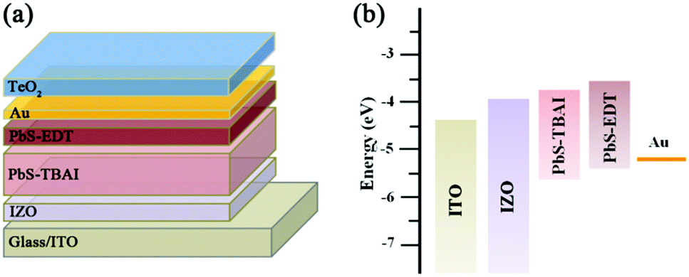 | ||
| Fig. 1 (a) Device architecture of the SCQDSC device. (b) Energy level diagram of the materials for the SCQDSC device.39,40 | ||
As demonstrated, when an ultrathin metal film is used alone as the back transparent electrode in the SSC devices, there is significant light reflection at the metal/air interface because of the refractive index mismatch, decreasing the optical transmittance of the SSC devices. For back transparent electrode preparation, a gold film with a thickness of 10 nm and a thin TeO2 antireflection capping layer were thermally evaporated in sequence to form complete SCQDSC devices (Fig. 1a).
2.2. Theoretical simulations
To understand the effect of the CQD solid and TeO2 antireflection capping layer on the optical properties and photovoltaic performance of the SCQDSCs, extensive theoretical modeling was carried out before experimental investigations. The opto-electric properties of the SCQDSCs with different thicknesses of the CQD solid and TeO2 capping layer were computationally modeled by using transfer matrix formalism (TMF).41–44 The complex refractive index [ñ = n(λ) + ik(λ)] of each layer in the SCQDSCs applied for TMF calculation was analyzed via spectroscopic ellipsometry, and is shown in Fig. S2 (ESI†) and in previous work.23 The results from the simulations are summarized in Fig. 2. Fig. 2a presents the visible transmittance spectra of the SCQDSCs without any capping layer and with different thicknesses of the TeO2 capping layer. It can be seen that enhanced transmittance was observed by covering the ultrathin Au film with a thin TeO2 capping layer, and that the transmittance of SCQDSC is strongly affected by the thickness of the TeO2 capping layer. By incorporating the high refractive index TeO2 layer on the ultrathin Au film, decreased light reflection at the interface of Au/air results, benefiting the transparency of SCQDSCs. However, the TeO2 capping layer with a high thickness will also increase the light absorption by the TeO2 layer and thus affect the transparency of the SCQDSCs in an opposite way. Therefore, an optimal balance between light reflection at the Au/air interface and absorption by the anti-reflective TeO2 capping layer is necessary for maximizing the transparency of SCQDSCs.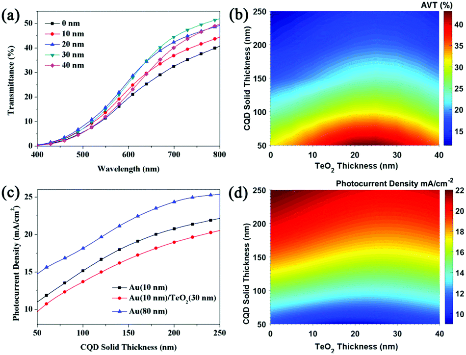 | ||
| Fig. 2 (a) Visible transmittance spectra of SCQDSCs without any capping layers and with different thicknesses of the TeO2 capping layer. (b) The effect of the CQD solid and TeO2 capping layer on the AVT of the SCQDSCs. (c) Photocurrent density of SCQDSCs with different back contact electrodes. The Au film with a thickness of 80 nm is applied for the fabrication of opaque CQD solar cells. (d) The effect of the CQD solid and TeO2 capping layer on the photocurrent density of SCQDSCs. During the optical and photovoltaic modeling, the thickness of the PbS-EDT layer in the SCQDSCs is 50 nm and the rested thickness is the PbS-TBAI layer. | ||
For different applications of SSCs, SSCs with various transparencies as a result of different thicknesses of the CQD solid in the device may be needed. Therefore, to figure out the influence of the TeO2 capping layer on the average visible transmittance (AVT) of SCQDSCs, CQD solid layers and TeO2 capping layers with various thicknesses were taken into account for AVT modeling, as shown in Fig. 2b. Clearly, a lower AVT is theoretically expected for SCQDSCs with a thick layer of the CQD solid due to increased light absorption from the CQDs.22 From the modeling, a TeO2 capping layer thickness of 20–30 nm is ideal for maximizing the transparency of the SCQDSCs, and with the thickness of the CQD solid increasing, a slightly thicker TeO2 capping layer is needed.
A trade-off between photovoltaic performance and transparency is general for all SSCs.9,45 However, at the maximum performance of the device all the light should ideally be absorbed in the CQD layer and other optical losses should be minimized. To understand the effect of the back transparent electrode on the photovoltaic performance of SCQDSCs, the photocurrent density of the SCQDSCs with a different back electrode was modeled according to a previously reported method.46 An opaque CQD solar cell with a thick Au film (80 nm) was also modeled for comparison, as shown in Fig. 2c. As expected, lower photocurrent density is observed for the SCQDSC with an Au (10 nm)/TeO2 (30 nm) electrode in comparison to that of the SCQDSC with only an Au (10 nm) electrode because of reduced light reflection at the Au/air interface, which leads to a lower optical electric field in the CQD layer and thereby a lower photocurrent. The opaque CQD solar cell with a back Au electrode of 80 nm exhibits a higher photocurrent density that is ∼5 mA cm−2 higher than that of the SCQDSC with an Au (10 nm)/TeO2 (30 nm) electrode, which implies that the back electrode is critical for an optimal solar cell performance. The optical electric field distribution versus position and incidence wavelength within the SCQDSC without any capping layers and with a TeO2 capping layer were also modeled, as shown in Fig. S3 (ESI†). The results show that a weaker intensity optical electric field was observed in the SCQDSC with a TeO2 capping layer due to lower light reflection at the Au/air interface. However, although the photocurrent is lowered the light transmission is significantly enhanced, which is necessary for use in SSCs.
Fig. 2d summarizes the dependence of the photocurrent density of SCQDSC on the CQD solid and TeO2 capping layer. Higher photocurrent is expected for the solar cell with a higher thickness of CQD solid. The photocurrent density is largely affected by the TeO2 capping layer and a slightly thicker TeO2 capping layer is necessary for SCQDSCs with a thicker CQD solid layer. The exciton generation rate within the CQD solid was further analyzed (Fig. S4, ESI†), showing that a lower exciton generation rate was obtained within the CQD solid after capping the ultrathin Au film with a TeO2 layer. This is expected due to the higher light transmission through the electrode and thereby higher transparency of the SSC. For the demonstrated SCQDSC with a given thickness of the CQD solid, a TeO2 capping layer with a thickness of 20–30 nm is optimal for balancing the decreased light reflection at the Au/air interface enabling a combination of high transparency and high photocurrent density.
2.3. Device performance
To compare with the results from the above simulations, SCQDSC devices were fabricated. Fig. 3a shows the cross-sectional scanning electron microscope (SEM) image of a complete SCQDSC device with a planar architecture of glass/ITO/IZO/CQDs/Au/TeO2. The transmittance spectra of SCQDSCs with various thicknesses of the CQD solid layer are presented in Fig. 3b. The thickness of the PbS-EDT layer in the CQD solid layer of all the devices is ∼50 nm. | ||
| Fig. 3 (a) Cross-sectional SEM image of the SCQDSC. (b) Transmittance spectra, (c) J–V curves, and (d) IPCE spectra of the SCQDSC with different thicknesses of the CQD solid. The thickness of the TeO2 capping layer is 30 nm. (e) The dependence of PCE and AVT on the thickness of the CQD solid. (f) Transmittance spectra and (g) J–V curves of the SCQDSC with different thicknesses of the TeO2 capping layer. (h) The dependence of PCE and AVT on the thickness of the TeO2 capping layer. The J–V curves were measured under AM1.5G illumination with a light intensity of 100 mW cm−2. | ||
It can be seen that the SCQDSCs exhibit good transmittance in the visible wavelength region, in good agreement with the modeled results in Fig. 2a. Lower transmittance is observed in the short wavelength region because of the high light absorption coefficient of PbS CQDs in this wavelength region.4 Decreased transmittance for devices with a thick CQD layer is obtained due to the fact that a CQD solid with a large thickness in the solar cell shows high light absorption.
Fig. 3c shows the measured photocurrent density–voltage (J–V) curves of SCQDSC devices prepared with different thicknesses of the CQD solid. The J–V curves were measured under AM1.5G 100 mW cm−2 illumination. The photovoltaic parameters as well as AVT are summarized in Table 1. When the SCQDSC has a CQD solid with a thickness of only 100 nm (PbS-TBAI 50 nm + PbS-EDT 50 nm) and an AVT of 31.4%, the device shows an impressive PCE of 5.0% with a short-circuit current density (Jsc) of 12.3 mA cm−2, an open-circuit voltage (Voc) of 615 mV and a fill factor (FF) of 0.66, respectively. For a CQD solid thickness of 200 nm (PbS-TBAI 150 nm + PbS-EDT 50 nm), the PCE was further enhanced up to 7.3% with a Jsc of 18.4 mA cm−2, a Voc of 605 mV, and a FF of 0.65, respectively, and the AVT lowers to 20.4%. The enhanced efficiency mainly stems from the improved photocurrent as a result of increased light absorption by the thicker CQD solid, which also leads to decreased optical transmittance. The results obtained from the experimental investigation were also compared to the results from simulations, which show that they are in good agreement (Fig. S5, ESI†).
| T CQD (nm) | T TeO2 (nm) | J sc (mA cm−2) | V oc (mV) | FF | PCE (%) | Average PCE (%) | AVT (%) |
|---|---|---|---|---|---|---|---|
| 100 | 30 | 12.3 | 615 | 0.66 | 5.0 | 4.9 ± 0.2 | 31.4 |
| 150 | 30 | 16.7 | 615 | 0.67 | 6.9 | 6.8 ± 0.2 | 23.9 |
| 200 | 30 | 18.4 | 605 | 0.65 | 7.3 | 7.1 ± 0.2 | 20.4 |
| 150 | 0 | 17.7 | 615 | 0.65 | 7.1 | 6.9 ± 0.1 | 17.5 |
| 150 | 10 | 17.1 | 620 | 0.66 | 7.0 | 6.8 ± 0.1 | 19.9 |
| 150 | 20 | 16.8 | 620 | 0.66 | 6.9 | 6.8 ± 0.2 | 22.8 |
| 150 | 40 | 16.3 | 615 | 0.66 | 6.7 | 6.6 ± 0.2 | 21.1 |
The corresponding incident photon to current conversion efficiency (IPCE) spectra are shown in Fig. 3d, with the SCQDSC having a thicker CQD solid showing a higher IPCE in line with the observed higher photocurrent density. To balance the device photovoltaic performance with transparency of the SCQDSC device, the PCE and AVT were measured for devices with different thicknesses of CQD solid, and the results are summarized in Fig. 3e. A trade-off is clearly observed between the device efficiency and transparency and, depending on the requested transparency, different efficiencies are obtained.
Fig. 3f displays the transmittance spectra of SCQDSCs without any capping layers and with different thicknesses (10–40 nm) of the TeO2 capping layer, and the corresponding AVT are also summarized in Table 1. After addition of a TeO2 capping layer on the SCQDSC device, the transmittance of the SCQDSC was largely enhanced so that the AVT is increased from 17.5% for the SCQDSC without any capping layers to ∼24% for the SCQDSC with a TeO2 capping layer thickness of 30 nm due to decreased reflection (Fig. S6, ESI†). The enhanced AVT of the SCQDSCs with a TeO2 capping layer may mainly result from the increased transmittance of the Au/TeO2 electrode (Fig. S7, ESI†).
Fig. 3g shows the J–V curves of the SCQDSCs without any capping layers and with different thicknesses of the TeO2 capping layer. The solar cell with a capping layer thickness of 30 nm shows a PCE of 6.9%, compared to that of 7.1% PCE of the solar cell without any TeO2 capping layer. The slightly lower PCE in this device is attributed to the reduced Jsc as a result of enhanced AVT and decreased light absorption in the CQD solid. Fig. 3h presents the effect of the TeO2 capping layer on the device efficiency and AVT. The results show that the thickness of the TeO2 capping layer is critical for the balance between the PCE with AVT because of the change in light reflection and light transmission at the Au/air interface. A thicker TeO2 capping layer is necessary to eliminate the light reflection at the Au/air interface, but the light absorption in the TeO2 layer also needs to be considered.
From the combination of theoretical modeling and experimental investigations, we conclude here that the optimal thickness of the TeO2 capping layer is around 30 nm for the demonstrated SCQDSCs by balancing the efficiency with transparency, in accordance with the results from simulations. We also compared these results with the widely studied semitransparent organic solar cells, which indicates that the SCQDSC demonstrated here shows comparable or even better photovoltaic performance and transparency than the semitransparent organic solar cells (Table S1, ESI†),8,15,47 and that the SCQDSC has great potential for semitransparent photovoltaics. Opaque CQD solar cells with an 80 nm-thick Au electrode were also fabricated for comparison. Solar cell devices with a CQD solid layer thickness of 100 nm, 150 nm and 200 nm demonstrated a PCE of 7.1%, 7.9% and 9.2%, respectively (Fig. S8 and Table S2, ESI†). For these opaque solar cells, we also find that a good agreement between the experimental results and the simulations (Fig. S9, ESI†), which indicates that the built model could offer practical and quantitative guidelines for CQD solar cell performance maximization.
2.4. Device stability
The stability of a SSC is important for the consideration of various applications, and therefore the stability of SCQDSCs under both continuous illumination and storage under ambient conditions was examined.The SCQDSC was placed under the solar simulator with continuous AM1.5G 100 mW cm−2 illumination and the test course was performed for 6000 s under a N2 atmosphere. Fig. 4a shows the evolution of efficiency, photocurrent density (JMPP) and voltage (VMPP) of the SCQDSC at the maximum power point (MPP) with continuous illumination. After illumination of ∼4500 s, the illumination was blocked by a shutter leaving the SCQDSC in the dark for ∼500 s, after which the shutter was opened again. It is encouraging that there is no significant degradation of the photovoltaic performance under continuous illumination. Both JMPP and VMPP maintain a high level output, resulting in ∼90% of the original PCE after illumination for ∼4500 s. The SCQDSC also exhibits good light response with the illumination on or off. It is notable that after the illumination is on again, a slightly higher PCE was recovered compared to just before the light was turned off, which indicates that the decreased efficiency with continuous illumination may be at least in part due to heating of the device during illumination and not from material degradation within the device. The device stability was also examined in an ambient atmosphere with continuous AM1.5G 100 mW cm−2 illumination. The results show that more than 90% of the original efficiency was maintained after illumination for ∼3100 s (Fig. S10, ESI†).
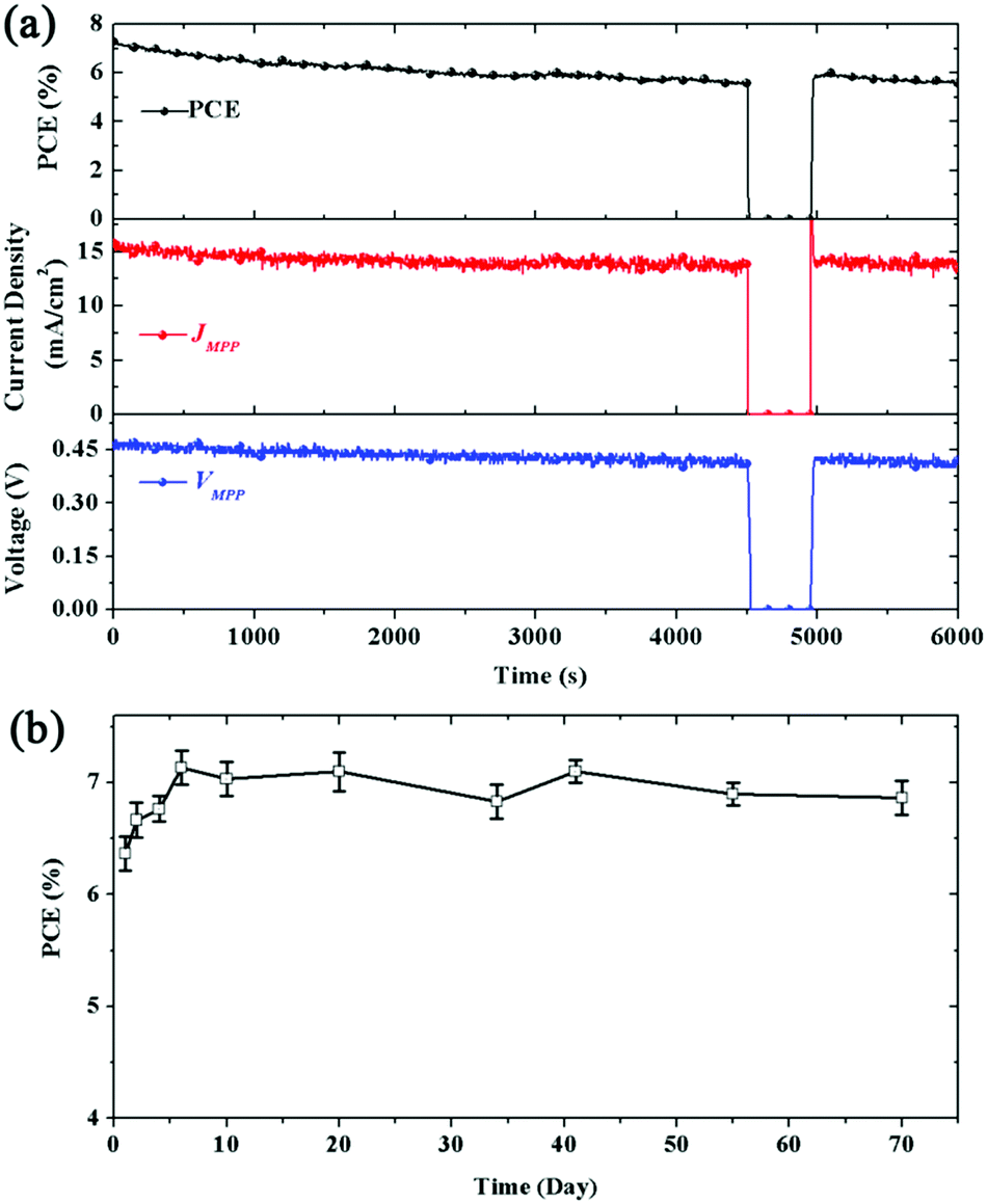 | ||
| Fig. 4 (a) Steady-state efficiency, photocurrent density and voltage of the SCQDSC at the MPP under continuous illumination of AM1.5G 100 mW cm−2. (b) Stability test of the unencapsulated SCQDSCs. The SCQDSCs were stored under ambient conditions. The thickness of the CQD solid and TeO2 capping layer is 200 nm and 30 nm, respectively. | ||
The unencapsulated SCQDSCs were stored in an ambient atmosphere. Fig. 4b shows the PCE as a function of storage time. It is interesting that the PCE is increasing in the initial 7 days and after 7 days the device maintains a high level performance with very small degradation. The reason for the increased PCE in the initial storage time is not clear at this point. Compared to the previous SCQDSCs,23 the stability of the demonstrated SCQDSCs is significantly enhanced, and the origin of the enhanced stability may be due to different CQD surface ligands and bilayer CQD device architecture, as reported by Bawendi.48 The increased stability may also be related to the extra TeO2 capping layer, which may reduce effects from the atmosphere.
2.5. Device color
Fig. 5a shows a photograph of the demonstrated SCQDSC. The final color of the SSC device should be considered for various applications, such as integration on buildings or windows. The transparency color perceptions of the SCQDSCs with different thicknesses of CQD solid were therefore calculated. Fig. 5b displays the color coordinates of the SCQDSCs with different thicknesses of CQD solid in the CIE1931 xy chromaticity diagram, which is designed to present the colors perceptible for the human eye.45,49 The AM1.5G solar spectrum was used for the color calculation and AM1.5G and reference D65 standard daylight illumination are also plotted for comparison. It can be seen that the color coordinates shift to the brown/red side in the chromaticity diagrams by increasing the thickness of the CQD solid. The brown/red appearance is due to the fact that the SCQDSCs with a thick CQD solid show stronger light absorption in the short wavelength in the visible region, leading to lower transmittance in these wavelength regions (Fig. 3b) and therefore higher transmittance of red light.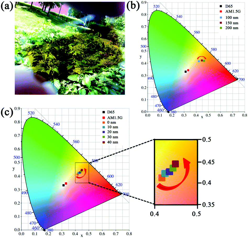 | ||
| Fig. 5 (a) Photograph of the demonstrated SCQDSC. (b) Color coordinates of the SCQDSCs with different thicknesses of the CQD solid under AM1.5G illumination on the CIE1931 chromaticity diagram. The thickness of the TeO2 capping layer is 30 nm. (c) Color coordinates of the SCQDSCs with different thicknesses of the TeO2 capping layer under AM1.5G illumination on the CIE1931 chromaticity diagram. The thickness of the CQD solid is 150 nm. The D65 standard daylight illumination and AM1.5G illumination are also plotted in the chromaticity diagram for comparison. | ||
To offer more details concerning the effect of the TeO2 capping layer on the transparency color of SCQDSCs, the transparency color of the SCQDSC without any capping layer and with different thicknesses of the TeO2 capping layer were also calculated. Fig. 5c shows the color coordinate of the SCQDSCs with different thicknesses of the TeO2 capping layer in the CIE1931 chromaticity diagram. The results show that the color of the SCQDSC is slightly affected by this capping layer. With the thickness of the TeO2 capping layer increasing, the color coordinates move to the yellow side.
2.6. Optical losses
For an ideal SSC, the incoming light is expected to be either absorbed by the light absorbing layer or transmitted through the complete device. However, the parasitic absorption induced by electrodes, charge transporting materials as well as reflection in the SSC device (Fig. 6a) lead to optical losses.12,23,50 Therefore, understanding the origin and amount of optical losses in the SCQDSC is necessary to fundamentally figure out the possibility of further improving the photovoltaic performance or transparency. A proportion spectrum of the incoming light in the SCQDSC was analyzed, as shown in Fig. 6b. It can be seen that most of the incoming light is either absorbed by the CQD solid or transmitted through the complete device in the visible region. Here, we define the optical efficient usage by the light absorbed by the CQD solid and the light transmitted through the complete device. Of course, other layers, such as ITO, IZO, Au, and the TeO2 capping layer, also absorb a certain proportion of the light in the visible region. The optical loss is defined by the light absorption by other layers in the device and reflection, as shown in Fig. 6c. It is found that the average optically efficient usage of the light in the visible region is up to ∼80%, which is largely enhanced compared to that of ∼60% of previously reported SCQDSCs.23 The improved optically efficient usage is therefore one of the main causes of the enhanced photovoltaic performance and transparency of the devices presented here.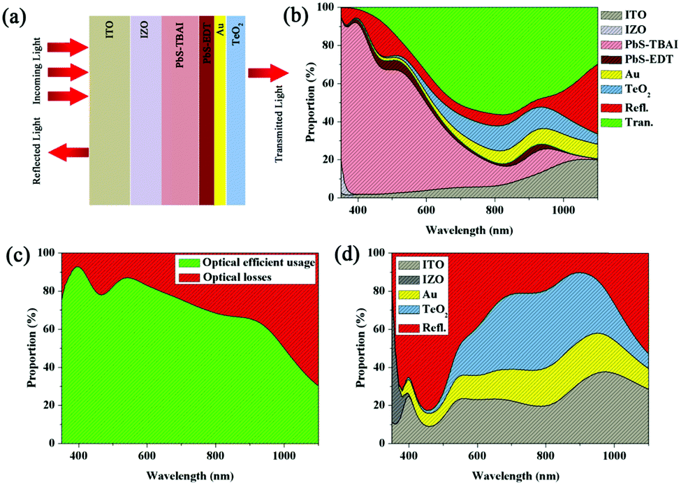 | ||
| Fig. 6 (a) Optical processes of the SCQDSCs. The incoming light is either absorbed by the materials within the SCQDSC, transmitted through the full device or reflected. (b) Proportion spectra of the incoming light in the SCQDSC. (c) Optically efficient usage and losses in the SCQDSC. (d) Proportion spectra of the optical losses by the reflection and absorption by ITO, IZO, Au and the TeO2 capping layer. | ||
The proportion of losses in each layer is also analyzed, as shown in Fig. 6d. It is found that the optical losses mainly stem from the light reflection in the short wavelength of the visible region. The total value of reflection and absorption by the TeO2 capping layer accounts for more than ∼40% of the optical losses in the longer wavelengths of the visible region. Therefore, further enhancement of photovoltaic performance and transparency is highly possible to be obtained by optical optimization of an antireflection layer or capping layer on the ultrathin metal electrode.
3. Conclusion
In summary, we have demonstrated highly efficient and transparent SCQDSCs through a combination of theoretical simulations and experimental investigations with new material combinations. The thickness of the CQD solid and the antireflective capping layer on the ultrathin metal electrode significantly affect the device photovoltaic performance and transparency. The optical losses in the SCQDSCs are largely decreased by optimization of the device architecture and in combination with a TeO2 capping layer on the ultrathin Au electrode, resulting in simultaneously enhanced photovoltaic performance and transparency. The SCQDSCs exhibit high PCEs of 7.3% with an average visible transmittance of 20.4%. Meanwhile, the SCQDSCs exhibit very good stability under both continuous illumination and storage under ambient conditions. These results suggest that PbS CQDs are very promising for high performing and stable semitransparent solar cells and the obtained SCQDSCs have potential for integration in buildings, windows or automobiles. The findings also provide practical and quantitative guidelines for further enhancing the photovoltaic performance and transparency of semitransparent solar cells.4. Experimental methods
4.1. CQD synthesis
PbS CQDs were synthesized according to the literature,51 and finally dispersed in octane with a concentration of ∼50 mg mL−1. The CQD solution was stored in an argon glovebox until usage.4.2. Device fabrication
SCQDSCs were fabricated on the ITO glass substrates (15 Ω □−1). The substrates were cleaned sequentially with water, acetone and ethanol with sonication for 20 min, and dried with air flow. The ITO substrates were UV-ozone treated for 20 min before depositing an IZO layer on the top of the ITO substrate. The IZO layer was prepared on the ITO glass substrate according to the reported method.39 Before deposition of the CQD layer on the top of the IZO layer, the IZO layer was subjected to UV-ozone treatment for 20 min. The CQD solution was filtered using a filter with a pore size of 0.2 μm and spin-coated on the top of the IZO layer at 2500 rpm for 13 s. The CQD film was treated with TBAI (10 mg mL−1 in methanol) for 30 s and then spun again at 2500 rpm. The treated film was rinsed with methanol twice. These processes were repeated until reaching the desired thickness. Another two CQD layers were deposited on the top of the PbS-TBAI film and treated with EDT (0.01 v/v% in acetonitrile) for 30 s. The film was rinsed 3 times with acetonitrile. An Au film with a thickness of 10 nm was thermally evaporated on the top of the CQD solid. The device was completed by thermal evaporation of the TeO2 capping layer on the Au film.4.3. Device characterization
The photovoltaic performance of the SCQDSC was measured using a Newport solar simulator (Model 91160) with AM1.5G illumination with a light intensity of 100 mW cm−2 (1 sun). Before the measurement, a certified reference Si solar cell (Fraunhofer ISE) was applied for light intensity calibration. The J–V curves of the SCQDSCs were measured using a Keithley model 2400 digital source meter under a nitrogen flow. The working area of the device was defined by a black mask with an aperture area of 6.8 mm2. IPCE spectra were recorded according to a previous method that uses a computer-controlled setup consisting of a xenon lamp (Spectral Products ASBXE 175), a monochromator (Spectral Products CM110), a LabJack U6, and a potentiostat (PINE, AFRDE 5).23 The transmittance spectra of the SCQDSCs were measured using an Ocean Optics HR2000 spectrometer with a Micropack DH-2000-BAL light source. Cross-sectional SEM images of the SCQDSCs were obtained using a scanning electron microscope (Zeiss 1550) at an accelerating voltage of 5 kV.4.4. Simulations
The optical properties of each material were measured using spectroscopic ellipsometry measurements with a Woollam VASE instrument over studied wavelengths and with different incidence angles. The ellipsometric data were analyzed by means of Kramers–Kronig consistent oscillator models. The transfer matrix method was applied for the simulation of the transmittance spectra of the SCQDSCs. The photocurrent density was modeled according to a previously reported method.46 Briefly, during the simulation, planar interfaces and isotropy were assumed for the layers within the SCQDSCs. The modeled photocurrent density was calculated by assuming 100% internal quantum efficiency and collection efficiency and an AM1.5G illumination spectrum was applied for the calculation.4.5. Device color calculation
The device color was calculated according to the literature.9 Briefly, the color calculation of the SCQDSC device is based on the determination of the CIE 1931 chromaticity coordinates x and y values, which were calculated from device transmittance T(λ) and CIE standard observer functions.Acknowledgements
This work was funded by Göran Gustafsson Foundation, Swedish Energy Agency, the Swedish Research Council FORMAS, ÅForsk, and the Swedish Research Council (VR). The authors thank Prof. Z. Hens, E. Drijvers, and Dr L. Häggman for discussion and technical support.References
- M. Yuan, M. Liu and E. H. Sargent, Nat. Energy, 2016, 1, 16016 CrossRef.
- E. H. Sargent, Nat. Photonics, 2012, 6, 133–135 CrossRef CAS.
- I. J. Kramer and E. H. Sargent, Chem. Rev., 2014, 114, 863–882 CrossRef CAS PubMed.
- G. H. Carey, A. L. Abdelhady, Z. Ning, S. M. Thon, O. M. Bakr and E. H. Sargent, Chem. Rev., 2015, 115, 12732–12763 CrossRef CAS PubMed.
- R. L. Wang, Y. Q. Shang, P. Kanjanaboos, W. J. Zhou, Z. J. Ning and E. H. Sargent, Energy Environ. Sci., 2016, 9, 1130–1143 CAS.
- M. A. Boles, D. Ling, T. Hyeon and D. V. Talapin, Nat. Mater., 2016, 15, 141–153 CrossRef CAS PubMed.
- X. Lan, O. Voznyy, F. P. Garcia de Arquer, M. Liu, J. Xu, A. H. Proppe, G. Walters, F. Fan, H. Tan, M. Liu, Z. Yang, S. Hoogland and E. H. Sargent, Nano Lett., 2016, 16, 4630–4634 CrossRef CAS PubMed.
- K.-S. Chen, J.-F. Salinas, H.-L. Yip, L. Huo, J. Hou and A. K. Y. Jen, Energy Environ. Sci., 2012, 5, 9551–9557 CAS.
- C. Roldán-Carmona, O. Malinkiewicz, R. Betancur, G. Longo, C. Momblona, F. Jaramillo, L. Camacho and H. J. Bolink, Energy Environ. Sci., 2014, 7, 2968–2973 Search PubMed.
- B. Petter Jelle, C. Breivik and H. Drolsum Røkenes, Sol. Energy Mater. Sol. Cells, 2012, 100, 69–96 CrossRef CAS.
- D. Zhang, K. Ryu, X. Liu, E. Polikarpov, J. Ly, M. E. Tompson and C. Zhou, Nano Lett., 2006, 6, 1880–1886 CrossRef CAS PubMed.
- Z. M. Beiley, M. G. Christoforo, P. Gratia, A. R. Bowring, P. Eberspacher, G. Y. Margulis, C. Cabanetos, P. M. Beaujuge, A. Salleo and M. D. McGehee, Adv. Mater., 2013, 25, 7020–7026 CrossRef CAS PubMed.
- J. H. Yim, S. Y. Joe, C. Pang, K. M. Lee, H. Jeong, J. Y. Park, Y. H. Ahn, J. C. de Mello and S. Lee, ACS Nano, 2014, 8, 2857–2863 CrossRef CAS PubMed.
- J. W. Jung, C.-C. Chueh and A. K. Y. Jen, Adv. Energy Mater., 2015, 5, 1500486 CrossRef.
- C.-C. Chen, L. Dou, J. Gao, W.-H. Chang, G. Li and Y. Yang, Energy Environ. Sci., 2013, 6, 2714–2720 CAS.
- M. Bonora, M. R. Wieckowsk, C. Chinopoulos, O. Kepp, G. Kroemer, L. Galluzzi and P. Pinton, Nat. Commun., 2015, 34, 1608 CAS.
- I. Moreels, K. Lambert, D. Smeets, D. De Muynck, T. Nollet, J. C. Martins, F. Vanhaecke, A. Vantomme, C. Delerue, G. Allan and Z. Hens, ACS Nano, 2009, 3, 3023–3030 CrossRef CAS PubMed.
- G. Itskos, P. Papagiorgis, D. Tsokkou, A. Othonos, F. Hermerschmidt, S. P. Economopoulos, M. Yarema, W. Heiss and S. Choulis, Adv. Energy Mater., 2013, 3, 1490–1499 CrossRef CAS.
- D. Zherebetskyy, M. Scheele, Y. Zhang, N. Bronstein, C. Thompson, D. Britt, M. Salmeron, P. Alivisatos and L. W. Wang, Science, 2014, 344, 1380–1384 CrossRef CAS PubMed.
- D. Tsokkou, P. Papagiorgis, L. Protesescu, M. V. Kovalenko, S. A. Choulis, C. Christofides, G. Itskos and A. Othonos, Adv. Energy Mater., 2014, 4, 1301547 CrossRef.
- I. Moreels, Y. Justo, B. De Geyter, K. Haustraete, J. C. Martins and Z. Hens, ACS Nano, 2011, 5, 2004–2012 CrossRef CAS PubMed.
- X. Zhang, G. E. Eperon, J. Liu and E. M. J. Johansson, Nano Energy, 2016, 22, 70–78 CrossRef CAS.
- X. Zhang, C. Hägglund, M. B. Johansson, K. Sveinbjörnsson and E. M. J. Johansson, Adv. Funct. Mater., 2016, 26, 1921–1929 CrossRef CAS.
- Y. M. Yang, Q. Chen, Y. T. Hsieh, T. B. Song, N. D. Marco, H. Zhou and Y. Yang, ACS Nano, 2015, 9, 7714–7721 CrossRef CAS PubMed.
- H. M. Stec, R. J. Williams, T. S. Jones and R. A. Hatton, Adv. Funct. Mater., 2011, 21, 1709–1716 CrossRef CAS.
- R. Betancur, P. Romero-Gomez, A. Martinez-Otero, X. Elias, M. Maymó and J. Martorell, Nat. Photonics, 2013, 7, 995–1000 CrossRef CAS.
- F. Guo, P. Kubis, N. Li, T. Przybilla, G. Matt, T. Stubhan, T. Ameri, B. Butz, E. Spiecker, K. Forberich and C. J. Brabec, ACS Nano, 2014, 8, 12632–12640 CrossRef CAS PubMed.
- L. Zuo, C. C. Chueh, Y. X. Xu, K. S. Chen, Y. Zang, C. Z. Li, H. Chen and A. K. Jen, Adv. Mater., 2014, 26, 6778–6784 CrossRef CAS PubMed.
- J. Huang, C.-Z. Li, C.-C. Chueh, S.-Q. Liu, J.-S. Yu and A. K. Y. Jen, Adv. Energy Mater., 2015, 5, 1500406 CrossRef.
- J. F. Salinas, H. L. Yip, C. C. Chueh, C. Z. Li, J. L. Maldonado and A. K. Jen, Adv. Mater., 2012, 24, 6362–6367 CrossRef CAS PubMed.
- H. W. Lin, S. W. Chiu, L. Y. Lin, Z. Y. Hung, Y. H. Chen, F. Lin and K. T. Wong, Adv. Mater., 2012, 24, 2269–2272 CrossRef CAS PubMed.
- C. Tao, G. Xie, C. Liu, X. Zhang, W. Dong, F. Meng, X. Kong, L. Shen, S. Ruan and W. Chen, Appl. Phys. Lett., 2009, 95, 053303 CrossRef.
- X. Zhang and E. M. J. Johansson, Nano Energy, 2016, 28, 71–77 CrossRef CAS.
- M. V. Kovalenko, Nat. Nanotechnol., 2015, 10, 994–997 CrossRef CAS PubMed.
- Z. Ning, O. Voznyy, J. Pan, S. Hoogland, V. Adinolfi, J. Xu, M. Li, A. R. Kirmani, J. P. Sun, J. Minor, K. W. Kemp, H. Dong, L. Rollny, A. Labelle, G. Carey, B. Sutherland, I. Hill, A. Amassian, H. Liu, J. Tang, O. M. Bakr and E. H. Sargent, Nat. Mater., 2014, 13, 822–828 CrossRef CAS PubMed.
- A. H. Ip, S. M. Thon, S. Hoogland, O. Voznyy, D. Zhitomirsky, R. Debnath, L. Levina, L. R. Rollny, G. H. Carey, A. Fischer, K. W. Kemp, I. J. Kramer, Z. Ning, A. J. Labelle, K. W. Chou, A. Amassian and E. H. Sargent, Nat. Nanotechnol., 2012, 7, 577–582 CrossRef CAS PubMed.
- M. Yuan, O. Voznyy, D. Zhitomirsky, P. Kanjanaboos and E. H. Sargent, Adv. Mater., 2015, 27, 917–921 CrossRef CAS PubMed.
- X. Zhang, Y. Justo, J. Maes, W. Walravens, J. Zhang, J. Liu, Z. Hens and E. M. J. Johansson, J. Mater. Chem. A, 2015, 3, 20579–20585 CAS.
- M. Liu, F. P. de Arquer, Y. Li, X. Lan, G. H. Kim, O. Voznyy, L. K. Jagadamma, A. S. Abbas, S. Hoogland, Z. Lu, J. Y. Kim, A. Amassian and E. H. Sargent, Adv. Mater., 2016, 28, 4142–4148 CrossRef CAS PubMed.
- C. H. Chuang, P. R. Brown, V. Bulovic and M. G. Bawendi, Nat. Mater., 2014, 13, 796–801 CrossRef CAS PubMed.
- C. C. Katsidis and D. I. Siapkas, Appl. Opt., 2002, 41, 3978–3987 CrossRef PubMed.
- L. A. A. Pettersson, L. S. Roman and O. Inganäs, J. Appl. Phys., 1999, 86, 487–496 CrossRef CAS.
- D. W. Sievers, V. Shrotriya and Y. Yang, J. Appl. Phys., 2006, 100, 114509 CrossRef.
- G. F. Burkhard, E. T. Hoke and M. D. McGehee, Adv. Mater., 2010, 22, 3293–3297 CrossRef CAS PubMed.
- G. E. Eperon, V. M. Burlakov, A. Goriely and H. J. Snaith, ACS Nano, 2014, 8, 591–598 CrossRef CAS PubMed.
- X. Zhang, C. Hägglund and E. M. J. Johansson, Adv. Funct. Mater., 2016, 26, 1253–1260 CrossRef CAS.
- C. C. Chen, L. Dou, R. Zhu, C. H. Chung, T. B. Song, Y. B. Zheng, S. Hawks, G. Li, P. S. Weiss and Y. Yang, ACS Nano, 2012, 6, 7185–7190 CrossRef CAS PubMed.
- X. Lan, S. Masala and E. H. Sargent, Nat. Mater., 2014, 13, 233–240 CrossRef CAS PubMed.
- G. E. Eperon, D. Bryant, J. Troughton, S. D. Stranks, M. B. Johnston, T. Watson, D. A. Worsley and H. J. Snaith, J. Phys. Chem. Lett., 2015, 6, 129–138 CrossRef CAS PubMed.
- J. M. Ball, S. D. Stranks, M. T. Hörantner, S. Hüttner, W. Zhang, E. J. W. Crossland, I. Ramirez, M. Riede, M. B. Johnston, R. H. Friend and H. J. Snaith, Energy Environ. Sci., 2015, 8, 602–609 CAS.
- X. Lan, O. Voznyy, A. Kiani, F. P. Garcia de Arquer, A. S. Abbas, G. H. Kim, M. Liu, Z. Yang, G. Walters, J. Xu, M. Yuan, Z. Ning, F. Fan, P. Kanjanaboos, I. Kramer, D. Zhitomirsky, P. Lee, A. Perelgut, S. Hoogland and E. H. Sargent, Adv. Mater., 2016, 28, 299–304 CrossRef CAS PubMed.
Footnote |
| † Electronic supplementary information (ESI) available. See DOI: 10.1039/c6ee02824a |
| This journal is © The Royal Society of Chemistry 2017 |