
 Open Access Article
 This Open Access Article is licensed under a
 Creative Commons Attribution 3.0 Unported Licence
Elimination of the light soaking effect and performance enhancement in perovskite solar cells using a fullerene derivative†
Shuyan
Shao
a,
Mustapha
Abdu-Aguye
a,
Li
Qiu
ab,
Lai-Hung
Lai
a,
Jian
Liu
a,
Sampson
Adjokatse
a,
Fatemeh
Jahani
b,
Machteld E.
Kamminga
a,
Gert H.
ten Brink
a,
Thomas T. M.
Palstra
a,
Bart J.
Kooi
a,
Jan C.
Hummelen
ab and
Maria
Antonietta Loi
*a
aZernike Institute for Advanced Materials, University of Groningen, Nijenborgh 4, 9747 AG, Groningen, The Netherlands. E-mail: m.a.loi@rug.nl
bStratingh Institute for Chemistry, University of Groningen, Nijenborgh 4, 9747 AG, Groningen, The Netherlands
First published on 2nd June 2016
Abstract
In this work, we investigate how electron extraction layers (EELs) with different dielectric constants affect the device performance and the light-soaking phenomenon in hybrid perovskite solar cells (HPSCs). Fulleropyrrolidine with a triethylene glycol monoethyl ether side chain (PTEG-1) having a dielectric constant of 5.9 is employed as an EEL in HPSCs. The commonly used fullerene derivative [60]PCBM, which has identical energy levels but a lower dielectric constant of 3.9, is used as a reference. The device using PTEG-1 as the EEL shows a negligible light soaking effect, with a power conversion efficiency (PCE) of 15.2% before light soaking and a minor increase to 15.7% after light soaking. In contrast, the device using [60]PCBM as the EEL shows severe light soaking, with the PCE improving from 3.8% to 11.7%. Photoluminescence spectroscopy and impedance spectroscopy measurements indicate that trap-assisted recombination at the interface between the hybrid perovskite and the EEL is the cause of the light soaking effect in HPSCs. The trap-assisted recombination is effectively suppressed at the perovskite/PTEG-1 interface, while severe trap assisted recombination takes place at the perovskite/[60]PCBM interface. We attributed these experimental findings to the fact that the higher dielectric constant of PTEG-1 helps to screen the recombination between the traps and free electrons. In addition, the electron donating side chains of PTEG-1 may also contribute to the passivation of the electron traps. As a consequence, the devices using PTEG-1 as the EEL display a considerable increase in the efficiency and a negligible light soaking effect.
Broader contextHybrid perovskite solar cells have witnessed unprecedented progress in power conversion efficiency from around 3% to around 22% in less than 10 years and have the potential to outperform silicon based solar cells, which took more than 20 years to achieve similar device performance and recently has reached a plateau. In addition, hybrid perovskites also have the advantages of being lightweight, processable on flexible substrates and possibly low cost. However, the rapid increase in device performance does not imply that hybrid perovskite solar cells do not present open issues; the large hysteresis presented by the current–voltage characteristics and their variation under illumination (light-soaking effect) raise concerns about the long-term operational stability of these solar cells. In this study we report that a high dielectric constant electron extraction layer (PTEG-1) helps to suppress the trap-assisted recombination at the perovskite/PTEG-1 interface and thus eliminates the light soaking effect and improves the device performance. |
1. Introduction
Hybrid halide perovskites (HPs) are regarded as promising materials for photovoltaic devices due to their high absorption coefficients, long diffusion length of free carriers, the non-excitonic nature of the photo-generated species, as well as the convenient solution processability.1–8 Over the past five years, intensive research efforts have been made to increase the power conversion efficiency (PCE) of methylammonium lead triiodide-type HP solar cells (SCs) to over 20% by developing strategies to improve the composition of the HP film and enable the film growth, and optimizing the interfacial layers and the device structure.4,9–20 However, the rapid increase in device performance is accompanied by several unresolved issues, such as the hysteresis of the current–voltage characteristics and the instability of the devices under continuous irradiation (light-soaking effect). Obviously, both effects raise concerns about the long-term operational stability of HPSCs.Nevertheless, the underlying mechanism of the light soaking effect is the reason for strong debates in the literature. Photoluminescence (PL) studies indicate that the trap states in HP layers are responsible for the light soaking effect.21,22 Some research groups attributed the light soaking to surface traps in the TiO2 electron extraction layer (EEL).23,24 Zhao et al. proposed that charges accumulated at the electrode interface and the positively charged bulk traps lead to severe loss in the open-circuit voltage (VOC) and fill factor (FF) of HPSCs using [60]PCBM as the EEL.25 In their model the photo-generated charges can neutralize these charges and thus increase the VOC and FF over time.25 Deng et al. proposed a doping mechanism to explain the light soaking phenomenon in device structures without EELs.26 They argued that the photo-generated voltage drives the positively/negatively charged ions to the cathode/anode electrodes, leading to p/n doping at the anode/cathode interface with a consequent increase in VOC.26 Recent computational studies indicate that metal halide perovskites are prone to form defects including vacancies, interstitial atoms, substituent atoms, and grain boundaries in the crystal structure.27–30
It is well known that defects in absorbers may play a critical role in determining the VOC of a solar cell. Defects that create deep energy levels usually act as Schockley–Read–Hall non-radiative recombination centers, leading to low VOC.29 Whereas, defects acting as shallow levels are benign to the device performance.29 In the case of MAI perovskite, the nature of traps is still subject to debate. Yin et al., by performing first-principles density-functional theory calculations, showed that the dominant intrinsic defects in HP are shallow traps.29 While Samiee et al., in mixed-halide based HPSCs, observed deep trap states (1023 m−3) with an activation energy of 0.6 eV below the conduction band.30 Baumann et al. also reported deep trap states in the order of 1021 m−3 in HPSCs by thermally stimulated current (TSC) measurements.31 Recently, trap density as low as 109–1010 m−3 was reported in HP single crystals, showing the role of the quality of the material in determining the trap density.32
A further point of consideration, which has been ignored until now in the HP literature, is the effect of the dielectric constant on the device performance. HPs have high dielectric constants with reported values higher than 6.5, which lead to very small binding energy of electron–hole pairs and generation of free carriers upon excitation.2,8,33,34 However, many organic charge carrier extraction layers, for example, [60]PCBM, usually feature a relatively low dielectric constant (≈3). Previous studies on polymer or polymer–inorganic nano-structured solar cells have proposed the dielectric mismatch to be unfavorable for charge separation at the organic/organic or organic/inorganic heterojunction interface.35–37
In this work, we investigate the effects of the dielectric constant of the EEL on the trap assisted recombination and light-soaking phenomena in HPSCs. The preparation of fulleropyrrolidine with a triethylene glycol monoethyl ether side chain (PTEG-1), having a dielectric constant of 5.9, was reported earlier.38,39 [60]PCBM, which has similar energy levels and a dielectric constant of 3.9, is used as a reference EEL.38,39 The device using PTEG-1 as the EEL shows a negligible light soaking effect, a starting PCE of 15.2%, which shows a minor increase to 15.7% after light soaking. In contrast, the device using [60]PCBM as the EEL shows severe light soaking, with the PCE increasing from 3.8% to 11.7%. Time-resolved and steady state photoluminescence combined with impedance spectroscopy measurements indicate that trap-assisted recombination is effectively suppressed at the perovskite/PTEG-1 interface, while severe trap assisted recombination takes place at the perovskite/[60]PCBM interface. The higher dielectric constant and electron donating properties of PTEG-1 may synergistically suppress the trap-assisted recombination at the HP/EEL interface. The reduction of the trap-assisted recombination has two major consequences, i.e., the increase of the efficiency and the almost total suppression of the light soaking effect. The stability of the electrical characteristics of the HPSC is an important pre-requisite for the technological exploitation of HPSCs.
2. Results and discussion
2.1. Device performance and light soaking effect
We fabricated devices with a p–i–n configuration ITO/PEDOT:PSS/CH3NH3PbI3−xClx/EEL/Al as shown in Fig. 1a. The fullerene derivative PTEG-1 with a dielectric constant of 5.9,38,39 and [60]PCBM with a dielectric constant of 3.9,38,39 are used to fabricate the electron-extraction layers. The chemical structures of these two EEL materials are shown in Fig. 1b.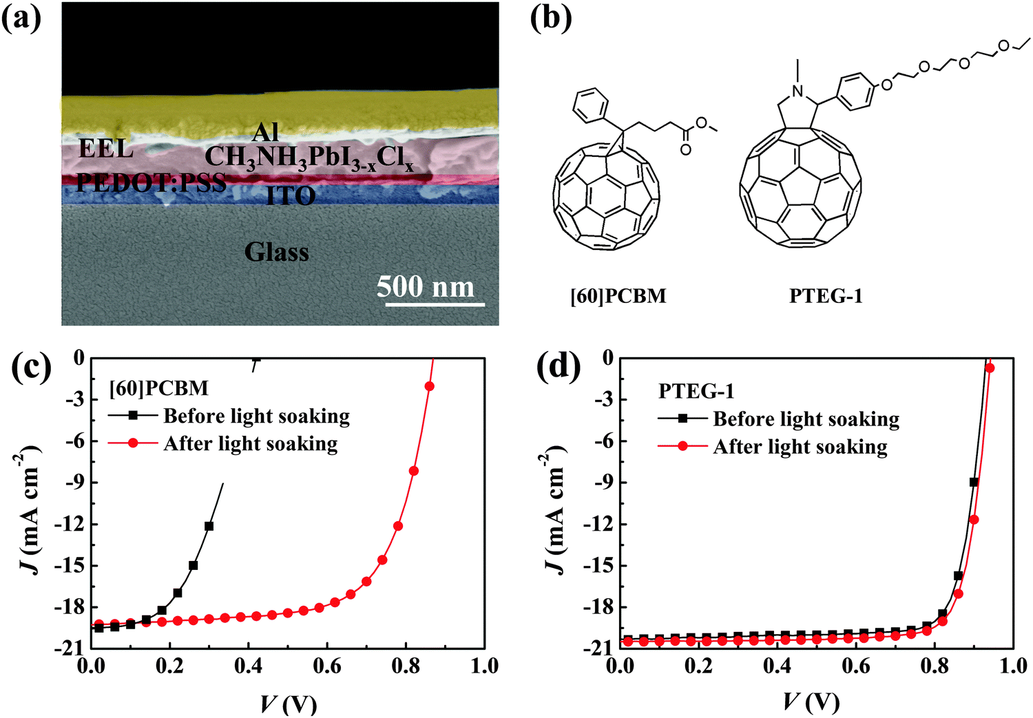 | ||
| Fig. 1 (a) Cross sectional SEM image of the device architecture, (b) chemical structures of [60]PCBM and PTEG-1. J–V characteristics under illumination for the devices using (c) [60]PCBM and (d) PTEG-1 as EELs. | ||
The performances of the devices using these two different EELs are investigated under continuous illumination. Before measurement, the devices were stored in the dark without applying any external bias. In the following, the condition under which the devices are measured immediately after exposure to the solar simulator is named ‘before light soaking’ and the condition under which the device is measured after reaching saturation with exposure to light is named ‘after light soaking’.
Fig. 1c and d show the J–V characteristics of the two (representative) devices fabricated using [60]PCBM and PTEG-1 as EELs, before and after light soaking. As can be seen from Fig. 1c, the reference device shows rather poor performance before light soaking, with a VOC of 0.42 V, a JSC of 19.50 mA cm−2, a FF of 0.46 and a PCE of 3.77% (see Table 1). After 1.5 h exposure to the solar simulator, it shows a considerable increase of its performance with a VOC of 0.87 V, a JSC of 19.20 mA cm−2, a FF of 0.70, and a PCE of 11.7%. Unlike the device using [60]PCBM as the EEL, the device using PTEG-1 shows very weak dependence on the light exposure time, as shown in Fig. 1d. Before light soaking, a VOC of 0.93 V, a JSC of 20.40 mA cm−2, a FF of 0.80 and a PCE of 15.2% are measured. After light soaking, a VOC of 0.94 V, a JSC of 20.63 mA cm−2, a FF of 0.81 and a PCE of 15.7% are measured. The J–V curve hysteresis for both devices is limited (see Fig. S1, ESI†). Fig. S2 and S3 (ESI†) show the statistics of the device parameters obtained for both device types. It is important to stress that regardless of light soaking, the device using PTEG-1 as the EEL shows considerably improved performance compared to that using [60]PCBM.
Fig. 2 summarizes how the device parameters for the two solar cells vary with time under continuous illumination. The VOC of the device using [60]PCBM as the EEL increases very fast from 0.42 to 0.8 V during the first 30 minutes, then slowly saturates after 1.5 h exposure to the solar light. While the JSC of the device is relatively constant, the FF follows the same trend as that of the VOC. Hence, the variation in PCE is mainly determined by that of the VOC and of the FF. For the device using PTEG-1 as the EEL, the VOC and FF increase slightly from 0.93 to 0.94 V, and 0.8 to 0.81, respectively.
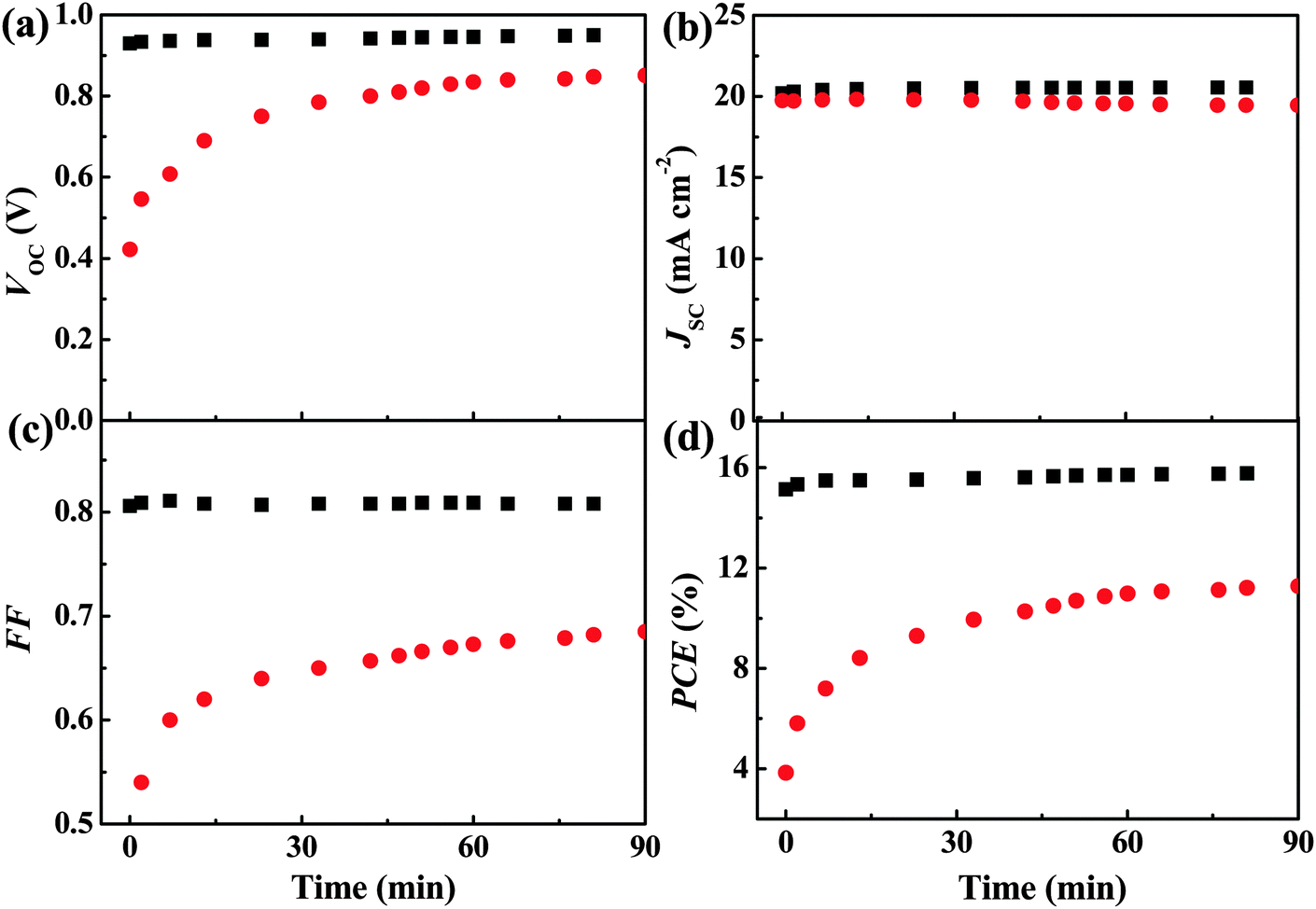 | ||
| Fig. 2 Time evolution of the (a) VOC, (b) JSC, (c) FF and (d) PCE of the device using PTEG-1 (black squares) and [60]PCBM (red dots) as EELs under illumination. | ||
Prolonged light illumination was carried out for the above soaked devices (see Fig. S4, ESI†) to detect their stability. After 9 hours of light exposure, the device using PTEG-1 as the EEL does not show observable degradation in the performance with a PCE of 100% of its initial value. Instead, the device using [60]PCBM as the EEL starts to show degradation after two hours of light exposure, and 82% of the initial PCE value is measured after 9 hours of light exposure. In the following sections, we focus on investigating the variation of the device parameters during the first 1.5 h of light soaking.
2.2. The origin of light soaking-trap assisted recombination
To explore the origin of the light soaking effect in HPSCs, we studied the light intensity dependence of the device performance before and after 1.5 h of light soaking. First we observed that the light soaking effect is reversible in HPSCs, and that the devices recover to their initial performance within 1.5 h storage under inert dark conditions.For devices measured before light soaking, the J–V curves were measured under varied light intensity with an interval of 1.5 h between each light intensity measurement; during the interval the devices were stored in a nitrogen filled glove box in the dark to recover their original state. For the devices measured after light soaking, the J–V curves were measured under varied light intensity sequentially without any extra storage in the dark.
Fig. S5 (ESI†) shows a logarithmic plot of JSC as a function of light intensity in the two device types. The slopes of JSCvs. light intensity are 1 for devices using [60]PCBM and PTEG-1 EELs before light soaking, indicating negligible bimolecular recombination.40 After light soaking, the slope values remain equal to 1, showing that bimolecular recombination is not involved in the light soaking phenomenon.
Fig. 3a and b shows a semi-logarithmic plot of the VOCvs. light intensity for the two device types. Ideally, the slope (n) of the curve should be equal to kT/q in the absence of trap assisted recombination.41 The device using [60]PCBM as the EEL measured before light soaking shows a slope of 1.70kT/q, demonstrating a significant energy loss from trap assisted recombination (Fig. 3a).35 After light soaking, the slope is reduced to 1.38kT/q, which is in agreement with the reduction of the trap-assisted recombination. For the device using PTEG-1 as the EEL, there is a limited variation of the slope from (1.23kT/q) to (1.18kT/q) as shown in Fig. 3b.
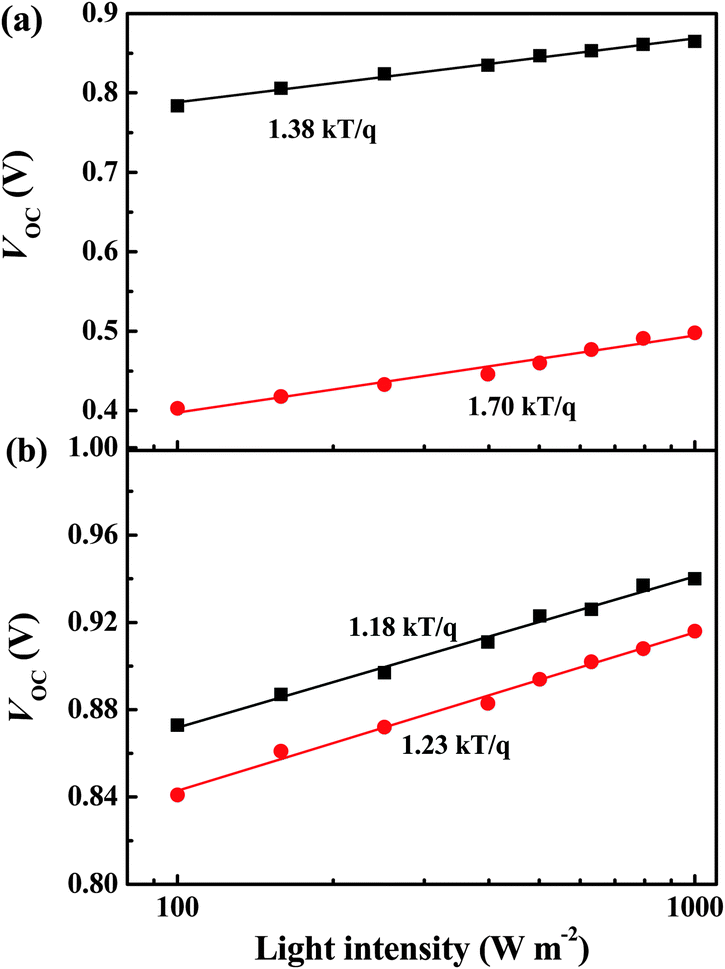 | ||
| Fig. 3 Light intensity dependent VOC for the devices using (a) [60]PCBM and (b) PTEG-1 as EELs before light soaking (in red) and after light soaking (in black). Symbols are experimental data and lines are the result of linear fitting. | ||
Therefore, PTEG-1 alleviates the trap-assisted recombination more effectively than [60]PCBM. Moreover, these results seem to indicate that the light soaking effect in HPSCs originates from trap-assisted recombination.
Impedance spectroscopy (IS) can further help to elucidate the bulk and interface properties of our devices.39,42Fig. 4 shows the time dependent Nyquist plots for the two types of devices measured under open circuit conditions under 1 Sun illumination. For devices which use [60]PCBM as the EEL, the Nyquist plots show asymmetric semi-arcs, probably due to the presence of a chemical capacitance (Cμ), which is possibly associated with the occupancy of the trap states at the HP/[60]PCBM interface.30 The semi-arcs get smaller, until saturation, with increasing light soaking time. This behavior can be fitted with the equivalent circuit shown in Fig. 4a, where RS is the series resistance; R1 and C1 are resistance and capacitance of the bulk HP layer, respectively. These parameters are not dependent on the light soaking time, which excludes either contact resistance or the bulk property of the HP layer as the reason for the light soaking effect. Instead, Cμ depends strongly on light soaking. After 1.5 hour light-soaking the chemical capacitance is significantly reduced, indicating a lower number of carrier traps at the HP/[60]PCBM interface (Fig. 4b). The reduced carrier recombination after light soaking causes smaller chemical resistance Rμ. Therefore, the smaller arc is due to higher carrier density in the device after trap filling under illumination. The fitting parameters are listed in Table S1 (ESI†).
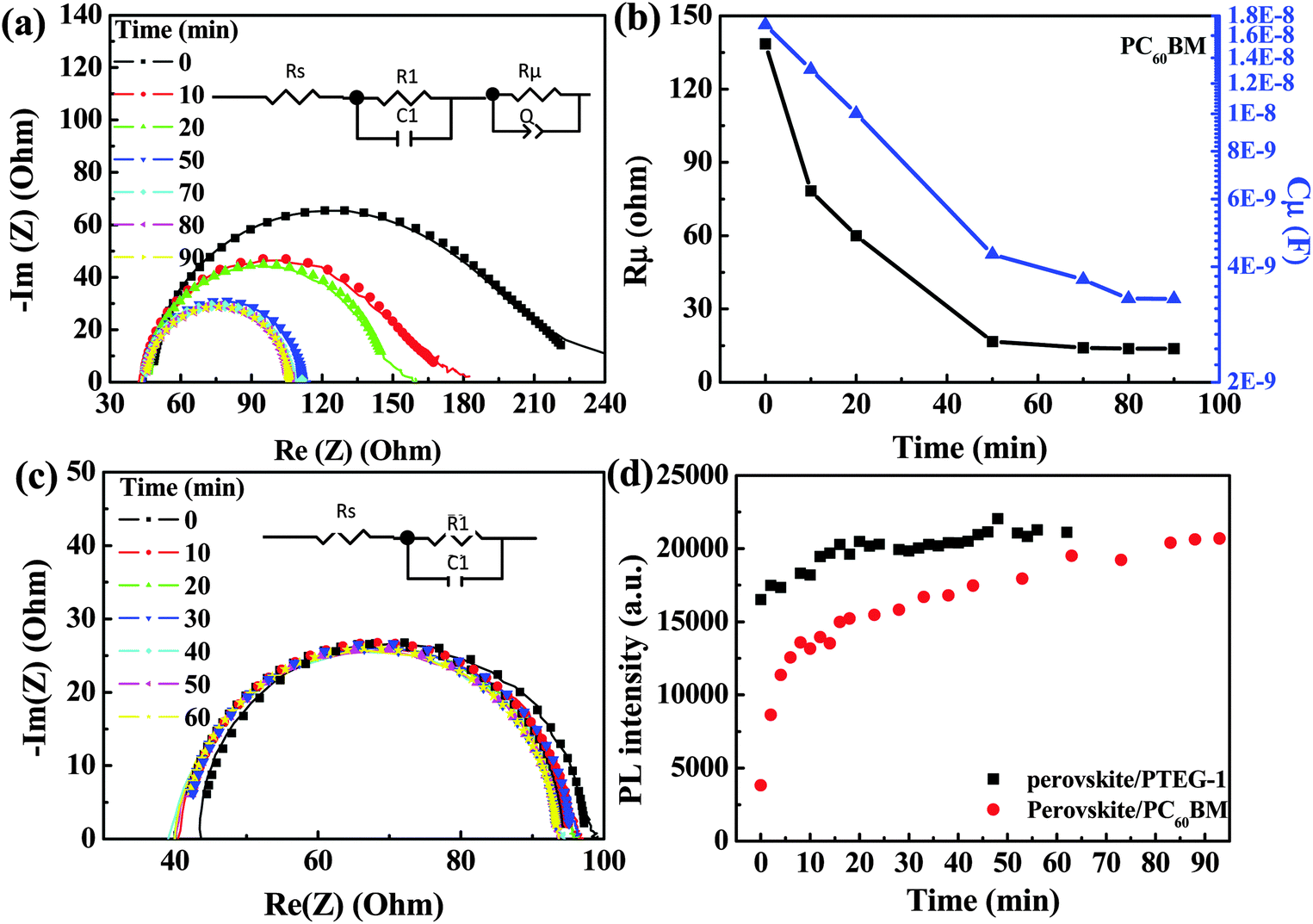 | ||
| Fig. 4 (a) Light soaking time dependence of the Nyquist plot (solid lines are experimental results and solid symbols are fitting results) and (b) Rμ and Cμ of the device using [60]PCBM as the EEL, (c) light soaking time dependence of the Nyquist plot of the device using PTEG-1 as the EEL, (d) variation of the PL intensity (detected at 780 nm) for ITO/PEDOT:PSS/perovskite/PTEG-1, and ITO/PEDOT:PSS/perovskite/[60]PCBM. | ||
Two distinctive features are observed in the impedance spectra of the device using PTEG-1 as the EEL. The symmetric semi-arcs, which are the classical features of an ideal semiconductor, could be fitted well with the simple equivalent circuit model shown in Fig. 4c. The absence of a considerable chemical capacitance indicates that the trap states at the HP/PTEG-1 interface are suppressed. Another important feature evidenced in Fig. 4c is that the shapes of the semi-arcs are very weakly dependent on the light soaking time. The fitting parameters used to reproduce these measurements are reported in Table S2 (ESI†).
The dark J–V characteristics of the corresponding devices measured before and after light soaking are displayed in Fig. S6 (ESI†). The exponential dependence of the current on the applied voltage, which is regarded as a typical property of a Shockley diode, is dominated mostly by the electron–hole recombination at the interface between the HP and the EEL.43 The turn-on voltage (the point where the current starts to increase exponentially) for the sample using [60]PCBM as the EEL before light soaking is only 0.4 V, while it increases considerably, reaching 0.8 V after light soaking (Fig. S6a, ESI†). The variation in turn-on voltage is consistent with that of the VOC which is observed under illumination. Before light soaking, the trap states could assist the recombination of carriers at the [60]PCBM/HP interface, as schematically illustrated in Fig. S2c (ESI†). A large number of trap states get filled during light soaking, strongly limiting the TA recombination pathway. At this point, charge carriers can only recombine in a bi-molecular pattern, which results in an increased turn-on voltage for the diode. The large variation in VOC indicates that the trap states might reside in the middle of the band-gap (deep traps).
In the HPSCs with PTEG-1 as the EEL, the turn on voltage shows negligible changes after light-soaking (see Fig. S6b, ESI†) due to suppressed trap-assisted recombination, which is in agreement with previous observations.41,44
Steady state PL measurements were performed in transmission mode on samples with a structure of ITO/PEDOT:PSS/HP/EEL, which were prepared under identical conditions to those for the device fabrication. Fig. 4d shows the variation in PL intensity recorded at the peak emission (780 nm) of the HP film excited at 400 nm at 295 K in a N2 atmosphere. The HP film with [60]PCBM as the EEL shows a fast and large increase in PL intensity within the first 30 min exposure to laser illumination and then saturates in about 1.5 hour. In contrast, the HP film with PTEG-1 as the EEL shows minor improvement in PL intensity over the same illumination time. It is important to underline that the rise time of the PL intensity matches that of the photo-voltage. It is also noted that HP/PTEG-1 samples emit light more effectively than the HP/[60]PCBM samples (see below). Recently, it has been predicted that the non-radiative decay of charge carriers is dominated by the deep-trap-assisted recombination.29 Our PL data further confirm that the deep electron trap-assisted recombination dominates the light soaking phenomenon.
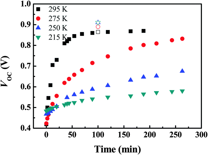
As mentioned above, the extremely slow photo-response of the performance of both devices and the as slow variation of the PL could be an indication of trap filling by mobile ions. To check this hypothesis, we investigated the temperature dependent VOC in HPSCs with the [60]PCBM EEL under continuous illumination, as shown in Fig. 5. As the temperature decreases, the increase in VOC slows down and after 90 minutes of light soaking, the VOC increases to 0.87, 0.7, 0.55 and 0.52 V at 295, 275, 250, and 215 K, respectively. As a comparison, the saturated VOC values of the device at those temperatures, but recorded after 90 minutes light soaking at 295 K, are shown by the open symbols in Fig. 5. The devices measured at lower temperatures exhibit an even higher saturated VOC value than that at 295 K. However, when the temperature is lower than 295 K, the VOCs are not saturated even after 4 h light soaking. The fact that the deactivation rate of the trap states becomes slower already at 275 K is indeed an indication that mobile ions are relevant for the trap filling process. Recent computational studies indicated that iodine vacancies have the lowest formation energy and these vacancies enable anion (I−) migration with a relatively low activation energy of about 0.6 eV.27,28,45 Therefore, we speculate that the positively charged iodine vacancies (V+I) act as electron traps in HPSCs and the mobile I− anions can fill them during light soaking.
 | ||
| Fig. 5 Time evolution of the VOC for the device using [60]PCBM as the EEL at different temperatures under continuous light illumination (solid symbols). Open symbols represent the saturated VOC values at various temperatures. | ||
Scanning electron microscopy (SEM) and atomic force microscopy (AFM) measurements were performed for the HPSC active layer before and after the deposition of the EELs. As shown in Fig. S7a and b (ESI†), the pristine HP layer is not compact, with large pinholes more than 100 nm in depth and with a consequent high surface roughness of about 34 nm. Such a rough HP film could have a very high density of deep traps due to the large grain boundaries, which may facilitate the formation of a high density of iodine vacancies. After [60]PCBM and PTEG-1 deposition, the active layer appears to be much smoother, with a roughness of about 9 and 14 nm, respectively (Fig. S7d–i, ESI†). It is interesting to note that the surface coverage of [60]PCBM is slightly better than that of PTEG-1, which excludes the EEL morphology as the factor determining the discrepancy in PCE and in suppressing the light-soaking phenomenon.
Time-resolved PL measurements could provide deeper insight into the influence of the trap states on the radiative decay dynamics. Fig. 6 shows the time-resolved PL decay measurements, taken at 780 nm, following the excitation at 400 nm of the samples with a structure ITO/PEDOT:PSS/HP/EEL, measured at 295 K. The pristine HP layer exhibits a mono-exponential PL lifetime of about 7.6 ns and when [60]PCBM and PTEG-1 are deposited on it the PL decay becomes bi-exponential. The faster decay is measured for the sample with [60]PCBM, which shows a pronounced first decay with a lifetime of 0.9 ns and a weaker component with a lifetime of about 11 ns. The PTEG-1 sample shows two components of similar intensity and with lifetimes of 1.9 ns and 5 ns. These experimental results indicate that the charge transfer process is much faster than the charge recombination process in the HP layer. Though the electron transfer from HP to [60]PCBM appears to be more efficient than that to PTEG-1, as we show in this work, the HPSCs using the [60]PCBM EEL suffer more severe TA recombination than the devices based on PTEG-1. Obviously, the severe trap-assisted recombination will open a new deactivation channel that should be evident in the dynamics of photoluminescence, explaining the faster decay time of the sample containing [60]PCBM.
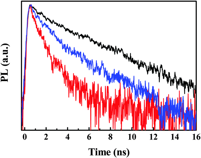 | ||
| Fig. 6 Time resolved PL before light soaking for ITO/PEDOT:PSS/CH3NH3I3−xClx (black line), ITO/PEDOT:PSS/CH3NH3I3−xClx/[60]PCBM (red line), ITO/PEDOT:PSS/CH3NH3I3−xClx/PTEG-1 (blue line). | ||
2.3. The light soaking effect suppression mechanism
In the previous section, we have shown that the light soaking effect is greatly reduced by using the fullerene derivative with higher εr, namely PTEG-1. In this part, we will discuss the possible mechanisms for the reduced light soaking effect from the molecular design perspective. Fig. 7a depicts the trap-assisted recombination process occurring between the perovskite layer and the EEL. The photo-generated electrons are first injected into the EEL and pile up at the perovskite/EEL interface before being collected at the cathode. These accumulated electrons before extraction at the cathode can be captured by surface traps in the perovskite layer ending up in non-radiative recombination.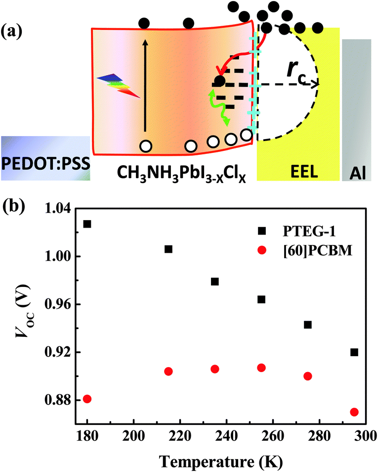 | ||
| Fig. 7 (a) Schematic of the proposed mechanism for the light soaking phenomenon, (b) VOCs measured after light soaking for the devices using [60]PCBM and PTEG-1 as EELs at different temperatures. | ||
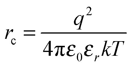
We propose as a possible mechanism the capture of electrons by interface traps driven by the Coulombic interactions between the electrons and the positively charged trap states on the HP surface. The critical distance (rc), at which the charges can escape the electrostatic force also with the aid of thermal energy (kT), can be expressed as follows:35
 | (1) |
Fig. 7b shows the temperature dependence of VOC in HPSCs using [60]PCBM and PTEG-1 as EELs. The HPSC using [60]PCBM as the EEL shows the maximum VOC value at 255 K. The trap density in perovskite film decreases as the temperature decreases,21,46 while the rc value increases according to eqn (1). At temperatures higher than 255 K, the reduced trap density dominates the trap-assisted recombination process. At temperatures lower than 255 K, the increased electrostatic binding force between the charges (rc = 20 nm at 215 K) dominates the recombination. Therefore the trade-off between the density of trap states and the electrostatic binding force results in a maximum VOC at 255 K. It is interesting to note that the HPSC using PTEG-1 as the EEL shows consistently increased VOC, with the temperature going down from 295 to 180 K. Owing to the higher dielectric constant of the PTEG-1 EEL, and assuming limited variation of it with temperature, the electrostatic force is not significantly increased even at low temperature (rc = 13 nm at 215 K). Thus, the reduced trap density at low temperature leads to significantly suppressed recombination and an increased VOC value.
Recently, Snaith et al. reported that Lewis bases may coordinate the halide vacancies and passivate these traps.47 It is noted that PTEG-1 has electron donating side chains consisting of a tertiary amine and triethylene oxide moieties, which may also coordinate with the iodide vacancies and thus passivate those electron traps.
Therefore, the high dielectric constant and electron donating properties of PTEG-1 may synergistically reduce the trap-assisted recombination and thus eliminate the light soaking phenomenon in HPSCs.
3. Conclusions
In conclusion, we investigated how the electron extraction material affects the device performance and the light soaking phenomenon in HPSCs. A high dielectric-constant (5.9) fullerene derivative PTEG-1 is used as an electron extraction layer and is compared with the most common and lower dielectric constant (3.9) fullerene derivative [60]PCBM. The power conversion efficiency of HPSCs using PTEG-1 as the electron extraction layer is about 15.7%, which is substantially higher than the 11.7% efficiency obtained using [60]PCBM. What is more important is that the device using PTEG-1 as the electron extraction layer shows a negligible light soaking effect compared to the devices using [60]PCBM, which are severely affected by light soaking. From the photoluminescence and impedance spectroscopy experiments, we learn that surface electron trap assisted recombination plays a dominant role in the light soaking effect. Therefore, it strongly affects the device performance. The higher dielectric constant of PTEG-1 helps to screen the recombination between the traps and the free electrons in the extraction layer. In addition, the electron donating side chains of PTEG-1 may passivate the electron traps. These two factors may synergistically improve the charge collection and reduce the light soaking effect.Experimental section
Materials
The MAI salt was synthesised from an equimolar mixture of MA (methylamine) and HI (hydriodic acid). A syringe was used to slowly add the hydriodic acid (57 wt% in H2O; Sigma Aldrich; 99.95%) to the methylamine solution (33 wt% in absolute alcohol; Sigma Aldrich), and the mixture was left under continuous stirring at 300 rpm for two hours. After evaporation at 70 °C, the prepared powder was washed five times with diethyl ether (Avantor) and a bright white powder was obtained. In order to dry, the salt was placed in a vacuum oven at 125 °C for 24 hours before storing in a nitrogen-filled glovebox. PbCl2 (99.99%), DMF (99.8%) and chloroform (99.8%) were acquired from Sigma-Aldrich.Device fabrication
ITO coated glass substrates were sonicated sequentially in a detergent, deionized water, acetone, and isopropanol for 20 minutes, respectively. After spin-drying, the cleaned ITO substrates were further dried at 140 degrees for 10 min. Then, the ITO substrates were subjected to UV ozone cleaning treatment for 20 min. A 30 nm thick PEDOT:PSS layer was spin coated onto the ITO substrates and dried at 140 degrees for 10 min. A precursor solution (40 wt%) of CH3NH3I and PbCl2 with a 3:1 molar ratio was spin-coated on top of PEDOT:PSS and then the substrates were stored in a high vacuum (<10−6 mbar) for 12 h. The annealing step was performed on the aforementioned substrates at 100 degrees for 1 h in a nitrogen-filled glove box. 280 nm thick CH3NH3PbI3−xClx films were obtained. Then, a 50 nm thick electron extraction layer was spin-coated on top of the perovskite films from solutions of [60]PCBM and PTEG-1. The device structure was completed by evaporating 100 nm thick Al under high vacuum <1 × 10⁻⁶ mbar.Characterization of perovskite solar cells
The current density–voltage characteristics of perovskite solar cells were measured under simulated AM 1.5 G solar illumination using a Steuernagel Solar constant 1200 metal halide lamp in a nitrogen filled glove box. The light intensity was calibrated to 100 mW cm−2 by using a calibrated Si cell.Steady-state and time-resolved PL measurements
The samples for the PL experiment were prepared in the same way as the devices, but without the deposition of the top electrode. These samples were measured in an inert atmosphere and excited at 400 nm by the second harmonic of a mode-locked Ti:sapphire (Mira 900) laser delivering pulses of 150 fs. Steady-state spectra were collected using a Hamamatsu EM-CCD camera and time resolved traces were recorded using a Hamamatsu streak camera working in single sweep mode.AFM measurements
The samples were prepared in the same way as that of the samples for the PL experiment. AFM topographical images were recorded in tapping mode using a Bruker MultiMode 8 microscope with TESP probes.SEM measurements
The same samples were used as that of the AFM measurement. SEM topographical images were recorded on a XL 30 ESEM microscope.Acknowledgements
This work is financed by the European Commission, Marie Curie Actions-Intra-European Fellowships (IEF) “SECQDSC” No. 626852 and European Research Council, ERC Starting Grant “HySPOD” No. 306983. The technical support of A. Kamp is highly appreciated. The authors would like to thank T. Sherkar and L. J. A. Koster for discussion. This is a publication of the FOM-focus Group ‘Next Generation Organic Photovoltaics’ No. 130, participating in the Dutch Institute for Fundamental Energy Research (DIFFER).Notes and references
- J. M. Ball, S. D. Stranks, M. T. Hörantner, S. Hüttner, W. Zhang, E. J. W. Crossland, I. Ramirez, M. Riede, M. B. Johnston, R. H. Friend and H. J. Snaith, Energy Environ. Sci., 2015, 8, 602–609 Search PubMed.
- Q. Lin, A. Armin, R. C. R. Nagiri, P. L. Burn and P. Meredith, Nat. Photonics, 2014, 9, 106–112 CrossRef.
- J. H. Heo, D. H. Song and S. H. Im, Adv. Mater., 2014, 26, 8179–8183 CrossRef CAS PubMed.
- N. Pellet, P. Gao, G. Gregori, T.-Y. Yang, M. K. Nazeeruddin, J. Maier and M. Grätzel, Angew. Chem., Int. Ed., 2014, 53, 3151–3157 CrossRef CAS PubMed.
- Y. Chen, J. Peng, D. Su, X. Chen and Z. Liang, ACS Appl. Mater. Interfaces, 2015, 7, 4471–4475 Search PubMed.
- S. D. Stranks, G. E. Eperon, G. Grancini, C. Menelaou, M. J. P. Alcocer, T. Leijtens, L. M. Herz, A. Petrozza and H. J. Snaith, Science, 2013, 342, 341–344 CrossRef CAS PubMed.
- G. Xing, N. Mathews, S. Sun, S. S. Lim, Y. M. Lam, M. Grätzel, S. Mhaisalkar and T. C. Sum, Science, 2013, 342, 344–347 CrossRef CAS PubMed.
- V. D’Innocenzo, G. Grancini, M. J. P. Alcocer, A. R. S. Kandada, S. D. Stranks, M. M. Lee, G. Lanzani, H. J. Snaith and A. Petrozza, Nat. Commun., 2014, 5, 3586 Search PubMed.
- A. Kojima, K. Teshima, Y. Shirai and T. Miyasaka, J. Am. Chem. Soc., 2009, 131, 6050–6051 CrossRef CAS PubMed.
- J. Burschka, N. Pellet, S.-J. Moon, R. Humphry-Baker, P. Gao, M. K. Nazeeruddin and M. Grätzel, Nature, 2013, 499, 316–319 CrossRef CAS PubMed.
- M. Cai, V. T. Tiong, T. Hreid, J. Bell and H. Wang, J. Mater. Chem. A, 2015, 3, 2784–2793 RSC.
- Z. Yuan, Z. Wu, S. Bai, Z. Xia, W. Xu, T. Song, H. Wu, L. Xu, J. Si, Y. Jin and B. Sun, Adv. Energy Mater., 2015, 5, 1500038 CrossRef.
- Q. Xue, Z. Hu, J. Liu, J. Lin, C. Sun, Z. Chen, C. Duan, J. Wang, C. Liao, W. M. Lau, F. Huang, H.-L. Yip and Y. Cao, J. Mater. Chem. A, 2014, 2, 19598–19603 RSC.
- H. Yu, X. Liu, Y. Xia, Q. Dong, K. Zhang, Z. Wang, Y. Zhou, B. Song and Y. Li, J. Mater. Chem. A, 2015, 321–326 Search PubMed.
- A. Mei, X. Li, L. Liu, Z. Ku, T. Liu, Y. Rong, M. Xu, M. Hu, J. Chen, Y. Yang, M. Grätzel and H. Han, Science, 2014, 345, 295–298 CrossRef CAS PubMed.
- J. Liu, S. Lu, L. Zhu, X. Li and W. C. H. Choy, Nanoscale, 2016, 8, 3638–3646 RSC.
- S. Bai, Z. Yuan and F. Gao, J. Mater. Chem. C, 2016, 4, 3898–3904 RSC.
- H.-S. Kim, C.-R. Lee, J.-H. Im, K.-B. Lee, T. Moehl, A. Marchioro, S.-J. Moon, R. Humphry-Baker, J.-H. Yum, J. E. Moser, M. Grätzel and N.-G. Park, Sci. Rep., 2012, 2, 591 CrossRef PubMed.
- M. M. Lee, J. Teuscher, T. Miyasaka, T. N. Murakami and H. J. Snaith, Science, 2012, 338, 643–647 CrossRef CAS PubMed.
- S. Shao, Z. Chen, H.-H. Fang, G. H. ten Brink, D. Bartesaghi, S. Adjokatse, L. J. A. Koster, B. J. Kooi, A. Facchetti and M. A. Loi, J. Mater. Chem. A, 2016, 4, 2419–2426 RSC.
- S. D. Stranks, V. M. Burlakov, T. Leijtens, J. M. Ball, A. Goriely and H. J. Snaith, Phys. Rev. Appl., 2014, 2, 034007 CrossRef.
- D. W. de Quilettes, S. M. Vorpahl, S. D. Stranks, H. Nagaoka, G. E. Eperon, M. E. Ziffer, H. J. Snaith and D. S. Ginger, Science, 2015, 348, 683–686 CrossRef CAS PubMed.
- Y. Li, Y. Zhao, Q. Chen, Y. (Michael) Yang, Y. Liu, Z. Hong, Z. Liu, Y.-T. Hsieh, L. Meng, Y. Li and Y. Yang, J. Am. Chem. Soc., 2015, 137, 15540–15547 CrossRef CAS PubMed.
- J. H. Heo, M. S. You, M. H. Chang, W. Yin, T. K. Ahn, S.-J. Lee, S.-J. Sung, D. H. Kim and S. H. Im, Nano Energy, 2015, 15, 530–539 CrossRef CAS.
- C. Zhao, B. Chen, X. Qiao, L. Luan, K. Lu and B. Hu, Adv. Energy Mater., 2015, 5, 1500279 CrossRef.
- Y. Deng, Z. Xiao and J. Huang, Adv. Energy Mater., 2015, 5, 1500721 CrossRef.
- A. Walsh, D. O. Scanlon, S. Chen, X. G. Gong and S.-H. Wei, Angew. Chem., Int. Ed., 2015, 54, 1791–1794 CrossRef CAS PubMed.
- J. M. Azpiroz, E. Mosconi, J. Bisquert and F. De Angelis, Energy Environ. Sci., 2015, 8, 2118–2127 Search PubMed.
- W.-J. Yin, T. Shi and Y. Yan, Appl. Phys. Lett., 2014, 104, 063903 CrossRef.
- M. Samiee, S. Konduri, B. Ganapathy, R. Kottokkaran, H. A. Abbas, A. Kitahara, P. Joshi, L. Zhang, M. Noack and V. Dalal, Appl. Phys. Lett., 2014, 105, 153502 CrossRef.
- A. Baumann, S. Väth, P. Rieder, M. C. Heiber, K. Tvingstedt and V. Dyakonov, J. Phys. Chem. Lett., 2015, 6, 2350–2354 CrossRef CAS PubMed.
- D. Shi, V. Adinolfi, R. Comin, M. Yuan, E. Alarousu, A. Buin, Y. Chen, S. Hoogland, A. Rothenberger, K. Katsiev, Y. Losovyj, X. Zhang, P. A. Dowben, O. F. Mohammed, E. H. Sargent and O. M. Bakr, Science, 2015, 347, 519–522 CrossRef CAS PubMed.
- D. Sapori, M. Kepenekian, L. Pedesseau, C. Katan and J. Even, Nanoscale, 2016, 8, 6369–6378 RSC.
- H.-H. Fang, R. Raissa, M. Abdu-Aguye, S. Adjokatse, G. R. Blake, J. Even and M. A. Loi, Adv. Funct. Mater., 2015, 25, 2378–2385 CrossRef CAS.
- M. Kuik, L. J. A. Koster, G. A. H. Wetzelaer and P. W. M. Blom, Phys. Rev. Lett., 2011, 107, 256805 CrossRef CAS PubMed.
- L. J. A. Koster, S. E. Shaheen and J. C. Hummelen, Adv. Energy Mater., 2012, 2, 1246–1253 CrossRef CAS.
- T. S. Sherkar and L. J. A. Koster, ACS Appl. Mater. Interfaces, 2015, 7, 11881–11889 Search PubMed.
- F. Jahani, S. Torabi, R. C. Chiechi, L. J. A. Koster and J. C. Hummelen, Chem. Commun., 2014, 50, 10645–10647 RSC.
- S. Torabi, F. Jahani, I. Van Severen, C. Kanimozhi, S. Patil, R. W. A. Havenith, R. C. Chiechi, L. Lutsen, D. J. M. Vanderzande, T. J. Cleij, J. C. Hummelen and L. J. A. Koster, Adv. Funct. Mater., 2015, 25, 150–157 CrossRef CAS.
- S. R. Cowan, R. A. Street, S. Cho and A. J. Heeger, Phys. Rev. B: Condens. Matter Mater. Phys., 2011, 83, 035205 CrossRef.
- G.-J. A. H. Wetzelaer, M. Scheepers, A. M. Sempere, C. Momblona, J. Ávila and H. J. Bolink, Adv. Mater., 2015, 27, 1837–1841 CrossRef CAS PubMed.
- J. C. Yu, D. Bin Kim, G. Baek, B. R. Lee, E. D. Jung, S. Lee, J. H. Chu, D.-K. Lee, K. J. Choi, S. Cho and M. H. Song, Adv. Mater., 2015, 27, 3492–3500 CrossRef CAS PubMed.
- S. R. Cowan, A. Roy and A. J. Heeger, Phys. Rev. B: Condens. Matter Mater. Phys., 2010, 82, 245207 CrossRef.
- Y. Shao, Y. Yuan and J. Huang, Nat. Energy, 2016, 1, 15001 CrossRef CAS.
- C. Eames, J. M. Frost, P. R. F. Barnes, B. C. O’Regan, A. Walsh and M. S. Islam, Nat. Commun., 2015, 6, 7497 CrossRef CAS PubMed.
- R. L. Milot, G. E. Eperon, H. J. Snaith, M. B. Johnston and L. M. Herz, Adv. Funct. Mater., 2015, 25, 6218–6227 CrossRef CAS.
- N. K. Noel, A. Abate, S. D. Stranks, E. S. Parrott, V. M. Burlakov, A. Goriely and H. J. Snaith, ACS Nano, 2014, 8, 9815–9821 CrossRef CAS PubMed.
Footnote |
| † Electronic supplementary information (ESI) available. See DOI: 10.1039/c6ee01337f |
| This journal is © The Royal Society of Chemistry 2016 |