Maximized performance of dye solar cells on plastic: a combined theoretical and experimental optimization approach†
Received
10th February 2016
, Accepted 29th March 2016
First published on 29th March 2016
Abstract
We demonstrate that a combined optimization approach based on the sequential alternation of theoretical analysis and experimental realization gives rise to plastic supported dye solar cells for which both light harvesting efficiency and electron collection are maximized. Rationalized configurations with optimized light trapping and charge extraction are realized to achieve photoanodes on plastic prepared at low temperature, showing a power conversion efficiency of 8.55% and a short circuit photocurrent of 16.11 mA cm−2, unprecedented for plastic based dye solar cell devices. Furthermore, the corresponding fully flexible designs present stable mechanical properties after several bending cycles, displaying 7.79% power conversion efficiency, an average broadband internal quantum efficiency above 90%, and a short circuit photocurrent of 15.94 mA cm−2, which is the largest reported value for bendable cells of this sort to date.
Broader context
Plastic based dye solar cells present several attractive features regarding their potential use as energy sources for portable rechargeable devices or in building integrated photovoltaics. One of them is beyond any doubt their low weight, which arises as a result of replacing partially or totally the thick glass slides that support the transparent conducting coatings usually employed. However, the efficiencies that can be achieved with these plastic based devices have traditionally been limited by the poor charge diffusion properties of the absorbing materials involved, which result from the low temperature processing of the absorbing materials, required to preserve the integrity of the plastic components. In this work we demonstrate a method to maximize the performance of plastic based dye solar cells based on an optimization procedure in which theoretical and experimental analyses are combined to reach the largest photocurrent achieved to date for these devices. This serves both to better rationalize the effect of each relevant parameter on their final efficiency and to pave the way for even further increasing their performance in the future.
|
Introduction
Flexible photovoltaic devices offer alternative, versatile, adaptable and scalable energy sources with high surface areas for both indoor and outdoor applications.1,2 They may replace the traditional installation approach by one based on the integration of the solar-to-electric energy conversion functionality into already existing structures, from windows to roofs, without adding load to the structures. New generation flexible solar cells can also present a wide range of color hues, which make them practical as elements of housing design. In this context, most photovoltaic technologies present today a branch devoted to the development of flexible energy conversion devices.3–9 The field of dye sensitized solar cells (DSCs) is not an exception.10 Several studies have reported on the development of bendable cells deposited on conducting metallic and plastic substrates.11,12 While a record certified power conversion efficiency (PCE) of 7.6% has been achieved,13 the average value in the field may be considered to be around 5.5%.14 These values, which are significantly lower than the record and average values attained for rigid DSCs,15 are due to the poor charge transport properties of nanocrystalline titania electrodes processed at low temperatures. With the aim of improving their photoconductivity, relevant advances have been made by the introduction of compression techniques,13 novel synthetic approaches that yield enhanced inter-particle connectivity,16 or original transfer methods for fabrication of completely transparent conducting oxide-free flexible cells with high efficiency.17 Another key aspect to be considered when optimizing the performance of a solar cell is light harvesting. In this regard, DSCs based on plastic substrates also have their particularities. A photoanode, in which the electron diffusion length is expected to be relatively short when compared to the electrode thickness, would benefit more, as recently demonstrated theoretically,18 from a specific light trapping scheme based on multiple scattering caused by high refractive index inclusions rather than by the presence of a diffuse back scattering layer, like the one typically employed in optimized DSCs on transparent conducting oxide (TCO) glass.19 The reason is that, in the former case, the electron generation function, which follows the optical absorption profile along the electrode,20 is increased in regions closer to the metal contact, thus enhancing electron collection efficiency. So far, no integral approach in which both a rigorous theoretical design and experimental realization are combined together in order to maximize light absorption and charge collection to achieve a high efficiency solar cell on a plastic substrate has been reported.
Herein, we propose and demonstrate a gradual optimization strategy of DSCs deposited on plastic substrates based on the sequential modeling and experimental evaluation of the optical and electrical properties of low temperature processed nanocrystalline titania electrodes. The result is that we are able to attain DSCs that display power conversion efficiencies (PCE) of 8.55%, when TCO glass is used as the counter-electrode, and a short circuit photocurrent (JSC) of 16.11 mA cm−2 under 1 Sun illumination, which is, to the best of our knowledge, the highest achieved on plastic substrates to date. Furthermore, in the case of fully flexible devices, when both substrates are made of plastic, a PCE of 7.79% and a JSC of 15.94 mA cm−2, also under 1 Sun illumination, are achieved, establishing a new JSC record for this sort of bendable device. The mechanical stability of the optimized flexible device is also analyzed, the same photovoltaic performance being retrieved after 180 bending cycles with a curvature radius of 15 mm. Unlike previous approaches, we use a systematic and gradual evaluation of the theoretical designs proposed at each optimization step by means of their experimental realization and characterization. This yields designs of increasingly better performance and provides at the same time a thorough physical insight into the optical and electrical properties of such devices. Maximum light absorptance is achieved by an optical scattering configuration in which TiO2 light scatterers of adequate size are randomly distributed at the right concentration within a photoelectrode. Simultaneously, electron collection is optimized by the incorporation of an intermediate layer with the same composition as the rest of the photoanode but without scatterers, whose role is to enhance the electrical contact between the electrode and the metal contacts without affecting the optimum optical absorption already achieved. A full description of the productive and parasitic absorption that occurs in different parts of the cell allows us to provide a reliable estimation of the internal quantum efficiency of the devices, which turns out to be around 90% over a wide spectral range.
Methods
Fabrication of dye-sensitized solar cells
For the fabrication of dye-sensitized solar cells, the autoclaved TiO2 (coined “autoTiO2”) nanoparticles are synthesized by slowly adding a mixture of titanium(IV) tetra-isopropoxide/2-propanol into distilled water in the presence of acetic acid, followed by gelation in an oil bath and hydrothermal processes in a titanium autoclave.21 Then, the synthesized autoTiO2 nanoparticles are collected by centrifugation and washed with EtOH three times, which are finally re-dispersed in a mixture of EtOH/tert-butanol (v/v = 50![[thin space (1/6-em)]](https://www.rsc.org/images/entities/char_2009.gif) :50) for use. The resulting autoTiO2 nanoparticles, which present a pure anatase phase and an average radius of about 10 nm, possess better electron transport and N719 dye adsorption properties than commercial Degussa P25 TiO2 nanoparticles. An inorganic binding agent, or nanoglue, was synthesized by the same sol–gel process as autoTiO2 but without the hydrothermal process in an autoclave,16 and following the same optimization method for its combination with commercial anatase particles within a hot compression procedure as recently demonstrated in ref. 22. Nanoglue containing anatase TiO2 particles of 2.5 nm radius were added into the organic binder-free paste to induce good interparticle connection at low temperature. Large TiO2 particles (T030, radius of 160 nm, K. K. Titan, Japan) were employed to give rise to multiple scattering within the electrode and hence enhance light harvesting at long wavelengths. The viscous organic binder-free paste made out of a combination of the three type of particles herein employed was formulated according to the typical procedure as follows: dispersed autoTiO2 particles, smaller particles of nanoglue, and T030 particles were mixed and further well-dispersed by tip sonication (Q500 Sonicator, Qsonica) and vigorous shaking using a vortex mixer for at least 10 min each step. The weight ratio of particles from autoTiO2, T030 and small particles of nanoglue is optimized at 55:30:15. The content of the particle mixture in final pastes was fixed at 15 wt%. A similar paste without adding T030 scattering particles was also prepared following the same procedure above for coating a thin adhesion layer which had a thickness of approximately (2.65 ± 0.15) microns and was employed to improve the electrical contact between the photoelectrode and the indium tin oxide (ITO) contact, differentiating itself from the well-known recombination blocking layer in the field of DSCs.
:50) for use. The resulting autoTiO2 nanoparticles, which present a pure anatase phase and an average radius of about 10 nm, possess better electron transport and N719 dye adsorption properties than commercial Degussa P25 TiO2 nanoparticles. An inorganic binding agent, or nanoglue, was synthesized by the same sol–gel process as autoTiO2 but without the hydrothermal process in an autoclave,16 and following the same optimization method for its combination with commercial anatase particles within a hot compression procedure as recently demonstrated in ref. 22. Nanoglue containing anatase TiO2 particles of 2.5 nm radius were added into the organic binder-free paste to induce good interparticle connection at low temperature. Large TiO2 particles (T030, radius of 160 nm, K. K. Titan, Japan) were employed to give rise to multiple scattering within the electrode and hence enhance light harvesting at long wavelengths. The viscous organic binder-free paste made out of a combination of the three type of particles herein employed was formulated according to the typical procedure as follows: dispersed autoTiO2 particles, smaller particles of nanoglue, and T030 particles were mixed and further well-dispersed by tip sonication (Q500 Sonicator, Qsonica) and vigorous shaking using a vortex mixer for at least 10 min each step. The weight ratio of particles from autoTiO2, T030 and small particles of nanoglue is optimized at 55:30:15. The content of the particle mixture in final pastes was fixed at 15 wt%. A similar paste without adding T030 scattering particles was also prepared following the same procedure above for coating a thin adhesion layer which had a thickness of approximately (2.65 ± 0.15) microns and was employed to improve the electrical contact between the photoelectrode and the indium tin oxide (ITO) contact, differentiating itself from the well-known recombination blocking layer in the field of DSCs.
The TiO2 films were coated using a doctor blade with 3 M tape as a spacer onto a transparent conducting plastic substrate (ITO/PEN, 200 μm thick, 15 Ω sq−1, transmittance of 80% at 550 nm, Peccell Tech. Inc.). TiO2 films were dried at ambient temperature and then simply hot compressed at 130 °C for 5 min using a lamination apparatus (Creative & Innovation System, Korea). To avoid contamination and film peeling off during compression, a thin Teflon film was inserted between the TiO2 film and the piston. Compressed films were then immersed into 0.5 mM N719 (cis-bis(isothiocyanato) bis(2,2′-bipyridyl-4,4′-dicarboxylato)-ruthenium(II) bis-tetrabutylammonium, Everlight) anhydrous ethanol solution for dye loading at 40 °C for 3 h with continuous shaking. For plastic cells, Pt counter-electrodes were prepared by spreading a drop of 7 mM of H2PtCl6·6H2O in 2-propanol on a glass substrate (FTO/glass, 8 Ω sq−1, 2.3 mm thick, Pilkington TEC8), and annealed at 400 °C for 20 min after being dried at ambient temperature. For fully flexible cells, a flexible counter-electrode consisting of Pt–Ti alloy on an ITO/PEN substrate (5 Ω square−1, 188 μm thickness) was purchased from Peccell Technologies Inc. The two electrodes were assembled using a 60 μm-thick hot melt Surlyn (Dupont 1702). The standard electrolyte solution was introduced through the drilled holes on the counter-electrode, which composed of 0.4 M tetrabutylammonium iodide (TBAI), 0.1 M LiI, 0.02 M I2, and 0.5 M 4-tert-butylpyridine (tBP) in acetonitrile. Unless otherwise indicated, the active area of dye-adsorbed TiO2 films was about 0.40 cm2, which was measured using an image analysis program equipped with a digital microscope camera (Moticam 1000). The thickness of TiO2 films was measured using an Alpha-step IQ surface profiler (KLA Tencor).
Photovoltaic characterization of dye-sensitized solar cells
The optical characterization of each component of the solar cell was carried out using an integrating sphere (Labsphere RTC-060-SF), a halogen lamp (Ocean Optics HL-2000) as a light source, and a spectrometer (Ocean Optics USB 2000+ UV-Vis) as a detector. Photocurrent-voltage measurements were performed using a Keithley 2400 source measure unit. A solar simulator (Yamashida Denso) equipped with a 1000 W Xenon lamp was used as a light source. Light intensity was adjusted employing an NREL-calibrated Si solar cell. A black mask with a proper aperture was placed on top of the cells to prevent the effect of diffuse light during measurement. The external quantum efficiency was measured using a system specifically designed for DSCs (PV measurements, Inc.).
For investigating the mechanical stability of the optimized flexible DSCs, the photovoltaic properties were recorded before and after various bending cycles (up to 180) using a cylindrical rod of radius 15 mm for the bending test.23
Optical modelling
For calculations, the same approach applied in ref. 24 was considered. It consists of a Monte-Carlo approach in which, for each wavelength, the trajectories of 107 photons impinging on the cell are considered. This number guarantees convergence for all computed output variables. The system involves a general multilayer structure in which each layer of a given thickness may comprise several materials (m), each one described by the corresponding complex spectral refractive index ñm(λ) = nm(λ) + ikm(λ), with λ the incident wavelength. In particular, from reflectance (R(λ)) and transmittance (T(λ)) measurements of simplified experimental samples of known thickness, the spectral ñm(λ) values of all materials here employed, including the dye and the electrolyte extinction coefficients, are extracted after applying the formalisms described in ref. 25–27. Specifically, the optical properties of the infiltrated mesoporous dye-sensitized TiO2 layer are defined in terms of a volumetric effective refractive index accounting for a 50% porous dye-sensitized TiO2 film infiltrated with an electrolyte,  . ñm(λ) spectra of all materials considered in the calculations are available in Fig. S1, ESI.† The trajectory of each individual photon is described by Fresnel coefficients at the interface of two layers, and by scattering Mie theory when photons interact with light scatterers. In this regard, the main novelty we introduced is the consideration of the influence of the external absorbing media on the diffuse dispersion of light described by Mie theory,28 something that was neglected in previously developed approaches in the field.15,29–32 To determine the trajectory of a photon, we calculate the distance l it travels before suffering either an absorption or a scattering event, through:
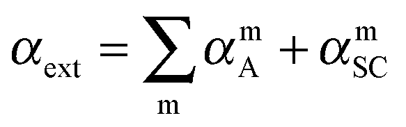
with r a random number fulfilling 0 < r ≤ 1, and αext the extinction coefficient accounting for both absorption (αmA) and scattering (αmSC) coefficients of all materials comprised in each layer:
For light scatterers, we define αscattererA = ρσscattererA and αscattererSC = ρσscattererSC with ρ = ffs(%)/Vscatterer the number density of the scatterers that depends upon the volume filling fraction (ffs(%)) and the scatterer volume (Vscatterer), and σscattererA and σscattererSC the corresponding single particle absorption or scattering cross sections calculated through Mie theory.28 For the remaining cell materials, αmA = 4πkm/λ and αmSC = 0. If the distance l travelled by the photon is larger than the possible distance it can cover in straight light before reaching the interface between two layers, the photon reaches the layer interface and it is transmitted or reflected back according to Fresnel coefficients. Those photons concluding their trajectory at the incoming or outgoing media contribute to reflectance and transmittance, and we can distinguish between diffuse and specular reflectance (Rd(λ) and Rs(λ), respectively) as well as diffuse and ballistic transmittance (Td(λ) and Tb(λ), respectively) through their exit angle. If the distance l travelled by the photon is shorter, either an absorption or scattering event occurs, and a new random number r′ is generated. If r′ ≤ αmSC/αext, the photon is scattered, and a new direction (θ, ϕ) is raffled according to the angular scattering distribution defined by Mie theory. Otherwise, the photon is absorbed by one of the absorbing materials contained in that layer, and the trajectory of the photon finishes. To determine the absorbing material, another random number is generated r′′ and it is compared to each of the absorption coefficients of all materials comprised in the layer, i.e., if r′′ ≤ αmA/αext, the photon is absorbed by material m. This allows us to specifically evaluate light absorbed by dye molecules within the electrode and therefore, evaluate the light harvesting of the cell ηLH(λ), separating it from electrolyte and scatterers absorptance. Moreover, parasitic absorption in the cell can be also evaluated. In addition, calculation of the trajectory of each photon provides spatial and spectral information of absorption events. This allows us to also evaluate the optical path or the distance covered by photons before absorption, as well as the electron generation function, or spectral absorption profile, g(λ, x), as the spatial location of all photons inside the cell is registered while the photon is travelling. The variable x is defined as the distance along the incident light propagation direction, with x = 0 set at the interface between the ITO and the nanocrystalline photoanode. Indeed, integration of g(λ, x) in x provides ηLH(λ), in which just the absorption of dye molecules is considered.
Therefore, as input parameters it is necessary to know the thickness of each layer in the structure, the filling fraction of the materials comprising each layer, the corresponding refractive indexes of all materials in each layer, and the particle radius if light scatterers are included. Importantly, with this model all optical magnitudes are evaluated without any fitting parameters.
Electrical modelling
Regarding the electrical part of the model, we assume an electron diffusion model like that originally proposed by Södergren et al. in ref. 20, and whose validity has been confirmed in numerous occasions afterwards. We assume, in a first approximation, that the electron recombination is linear, and take as the only fitting parameter the ‘effective’ electron diffusion length, Le, that accounts for the average distance covered by the electron before recombination.18 This is the simplest electrical model to be employed in which all microscopic (intra-grain) and mesoscopic (inter-grain) electron transportation processes are gathered together in Le (without the chance of discriminating processes). The ηEQE(λ) is affected by four partial efficiencies, namely, light harvesting efficiency (or absorptance) ηLH(λ), electron collection efficiency ηcol(λ), electron injection efficiency ηinj(λ), and dye regeneration efficiency ηreg(λ):| | |
ηEQE(λ) = ηLH(λ)ηcol(λ)ηinj(λ)ηreg(λ)
| (1) |
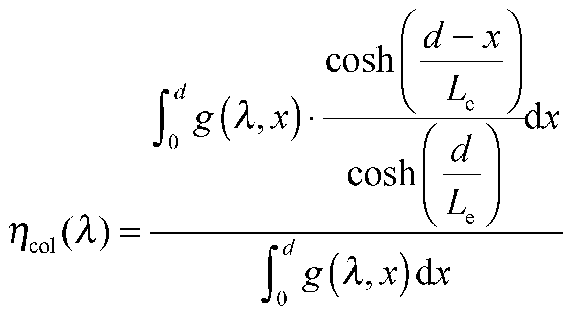
Collection efficiency is determined by spatial integration of the electron generation function weighted by the fitting parameter Le:
| |
 | (2) |
where
d is the total electrode thickness. Electron collection is thus herein considered as a result of electron diffusion through the nanocrystalline network and the transfer to the ITO and, from there, to the metal contact. In addition, our full optical and electrical model allows evaluating the internal quantum efficiency
ηIQE(
λ) defined as:
| | |
ηIQE(λ) = ηEQE(λ)/ηLH(λ) = ηcol(λ)ηinj(λ)ηreg(λ)
| (3) |
Moreover, since the inclusion of light scatterers within the photoelectrode affects both ηLH(λ) and ηcol(λ), while it can be assumed that it has a negligible effect on the injection and regeneration efficiencies, we can take ηinj(λ) = ηreg(λ) = 1 rendering the internal quantum efficiency and charge collection efficiency equivalent:
| | |
ηIQE(λ) = ηEQE(λ)/ηLH(λ) = ηcol(λ)
| (4) |
All predictions and fittings herein presented have been carried out using this model.
Results and discussion
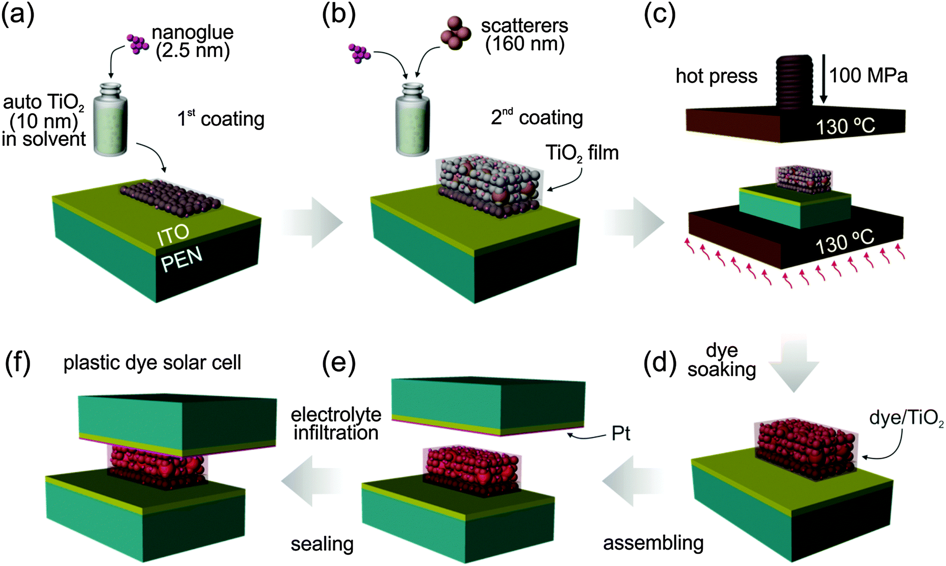
In what follows we will describe the optimization procedure followed to obtain a highly efficient flexible solar cell, maximizing light harvesting and electron collection by introducing gradual changes in the electrode structure. Our optimization approach is based on the sequential maximization of optical absorption and charge transport in four steps: first a reference DSC on a plastic substrate with a rigid counter-electrode is devised; second, TiO2 scatterers of optimal size and concentration are randomly distributed within the electrode to enhance light absorption; third, electron collection is enlarged by including an intermediate adhesion layer between the contact and the electrode of the previous DSC already optimized optically; and finally, the rigid counter-electrode is replaced with a plastic film to realize the fully flexible version. Partial results of each of the optimization steps just mentioned will be shown along this work. As a result of this study, we reach a final experimental procedure to attain the optimum design of a highly efficient mechanically stable flexible DSC, which constitutes one of the main contributions of our work and is schematized in Fig. 1. First, a thin layer (<3 microns) made of low sintering temperature nanocrystalline titania is deposited on an ITO coated plastic substrate (Fig. 1a) in order to maximize the electrical contact between the photoanode and the transparent conductor; on top of this, a titania film containing a multimodal distribution of crystals with sizes in three well defined ranges, so that they can serve to build a chemically glued mesostructure containing light scatterers, is casted (Fig. 1b); hot compression (Fig. 1c) and dye soaking of the film (Fig. 1d) follows; finally, a platinized conducting plastic substrate is added as a counter-electrode (Fig. 1e), and the electrodes are hot sealed with a thermoplastic (Fig. 1f).
 |
| | Fig. 1 Schematic illustration of the final fabrication process of a plastic dye solar cell on a flexible ITO/PEN substrate containing the necessary optimization steps. (a) A thin adhesion layer was coated using the doctor blade method with 3 M tape as a spacer from an organic binder free paste which was prepared by dispersing 2.5 nm radius nanoglue nanoparticles (NPs) with 10 nm radius TiO2 NPs into the mixture solvent of EtOH and tert-butanol. (b) Main TiO2 layer was coated using the same method but with a 160 nm radius scattering NP added paste. (c) Hot pressing, that is, physically pressing at 100 MPa simultaneously with heating at 130 °C to synergistically enhance the interconnection of TiO2 NPs. (d) Dye soaking of TiO2 film. (e) Electrolyte infiltration, and assembling dye sensitized TiO2 film with a thermoplastic surlyn and a counter electrode composing of a catalytic Pt layer on an ITO/PEN substrate. (f) Hot sealing of electrodes by thermoplastic surlyn for a plastic dye solar cell. | |
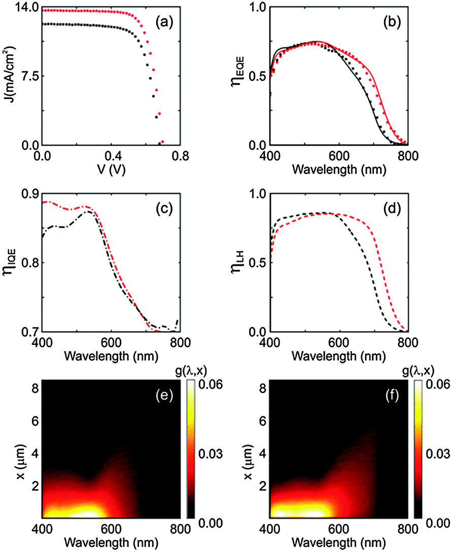
Each modification in the electrode structure was realized following the guidelines extracted from a detailed electrical and optical theoretical model of the cell, whose full description can be found in the Methods section. In brief, it consists of a Monte Carlo approach in which the trajectory of individual photons defined by Fresnel coefficients at the interface of two material layers, and scattering Mie theory when light scatterers are considered, is fully accounted for. By collecting all photons concluding their trajectory at the incoming or outgoing media, we can evaluate reflectance and transmittance and distinguish diffuse light through their exit angle. Those photons finishing their trajectory inside the DSC contribute to the absorption of the cell, our model being capable of discriminating between productive (photons absorbed by dye molecules) and parasitic (photons absorbed by any other material comprising the cell) absorption. With our model we can evaluate all optical magnitudes not only spectrally but also spatially (inside each component of the cell) thus yielding the electron generation function (or spectral absorption profile) g(λ, x) and, most importantly, without employing any fitting parameters. Concerning the electrical magnitudes, the only fitting parameter enters the model via the electrical part, when the external quantum efficiency ηEQE(λ) is calculated through an ‘effective’ electron diffusion length, Le, that accounts for the average distance covered by the electron before recombination. This theoretical model was first employed to evaluate the reference cell, i.e., without any kind of electrode structuring and/or light scatterers. Such DSCs were prepared on standard conducting plastic substrates, namely ITO coated polyethylene naphthalate (ITO-PEN), following a combination of chemical and physical sintering.22 This method relies on the use of a bimodal distribution of particles in the precursor paste, the smaller ones being of the order of a few nanometers and the larger with an average size of around a few tens of nanometers. The former ones serve as a sort of nanoglue capable of enhancing the connectivity, and hence the electrical and mechanical properties, of the photoanode.16 The compression at low temperature of this paste results in the formation of a mesoporous film with improved charge transport properties. In our case, and in order to maximize the efficiency with photoanodes built by this method, we use autoclaved nanocrystalline titania particles (autoTiO2), following a procedure, as described in the Methods section, which provides films with better dye adsorption and charge transport properties than commercial particles.33 Besides, a highly transparent electrolyte is prepared to minimize parasitic absorption losses in the cell. The results of the photovoltaic characterization of solar cells containing these compressed nanoglued photoanodes of approximately (8.60 ± 0.05) microns are presented in Fig. 2. Analysis of the current density–voltage (J–V) curve of the reference cell prepared using this combined chemical and physical sintering method, displayed as a black square curve in Fig. 2a, yields an overall PCE of 5.94%. Although it is a relatively high value for a transparent cell, the analysis of these first cells unconcealed the need of improving both light harvesting and electron collection in order to enhance the performance of the plastic substrate based device. Indeed, a first look at the ηEQE(λ) plotted as black squares in Fig. 2b reveals that light absorption of the dye is meaningful, but it is still inefficient in the wavelength range above 600 nm. Using our model, we evaluate ηEQE(λ), ηIQE(λ) and ηLH(λ) for the same reference cell. All magnitudes are displayed in Fig. 2b, c and d as solid, dashed and dash-dotted lines, respectively. From the fitting of ηEQE(λ) and the calculation of ηLH(λ) we notice that, while light absorption by the dye is close to saturation for blue and green photons, it drops significantly for red ones. Also, the estimated ηIQE(λ) (or equivalently ηcol(λ)) is around 85% for the former and only 70% for the latter, revealing that charge collection is not optimal and that it presents significant wavelength dependence. This is characteristic of electrodes in which the electron average diffusion length is shorter than the one required to effectively collect all photocarriers, hence being charge collection very sensitive to the precise profile of the electron generation function, g(λ, x), which is plotted in Fig. 2e. In this contour plot it can be readily seen that red photons are absorbed at longer distances from the metal contact as a result of the smaller absorption coefficient of the dye at those wavelengths, their absorption being therefore more affected by a short Le. In fact, the best fit of ηEQE(λ) for the reference cell is found for Le = 8 microns. Although this is a respectable value for a non-thermally sintered electrode, our model allows us to identify it as mainly responsible, along with the observed insufficient long wavelength absorption, for the limited performance of the device of reference.
 |
| | Fig. 2 (a) Experimental J–V curves of plastic cells. Square black symbols correspond to an (8.60 ± 0.05) micron electrode without scatterers, and circular red ones to an electrode of the same thickness with 30% of titania particles of radius 160 nm. (b) Experimental (symbols) and theoretical (solid lines) ηEQE(λ) spectra for the same systems as in panel (a). The “effective” electron diffusion length is taken to be Le = 8 microns. (c) Corresponding calculated ηIQE(λ) (or equivalently ηcol(λ)) curves and (d) ηLH(λ) (or absorptance) spectra. (e and f) Electron generation functions, or spectral absorption profiles g(λ, x) of each photoelectrode as a function of x and λ for a (e) reference cell without scatterers and (f) a DSC with 30% of light scatterers (r = 160 nm). | |
In order to tackle the low red photon absorption observed, we employed an optimization procedure based on the evaluation of numerous optical configurations. Both back diffuse scattering layers and intra-electrode multiple scattering configurations were theoretically analyzed (Fig. S2 in the ESI†). In this latter case, a wide range of spherical titania particle radius and concentrations were considered, and different electrode thicknesses covering the experimental error were compared. The response of systems differing by 50 nm in thickness was the same. Best results were attained for those configurations in which light harvesting is augmented as a result of light trapping caused by multiple scattering due to inclusions in the nanocrystalline photoanode. Calculations also showed that this approach presents a high degree of tolerance, as a wide range of particle sizes (between 100 nm and 200 nm radius) and concentrations (filling fractions ffs between 10% and 30%) gave rise to similar absorption enhancements (Fig. S3 and S4 in the ESI†). Upper limits of particle concentration are not absolute, as the model is not applicable for concentrations above 30%. Moreover, our theoretical analysis shows that the use of structured electrodes with a multilayer architecture,12 in which the concentration of light scatterers is gradually increased as the incident light enters the electrode, yields slightly less efficient cells than those made of electrodes containing just a single concentration of scatterers (Fig. S4 in the ESI†). This is more clearly seen through the analysis of the solar spectrum weighted integrated absorption (ηsswia), defined as the fraction of light absorbed by dye molecules weighted across the solar spectrum (AM1.5), between 400 and 800 nm
| |
 | (5) |
With this definition, the
ηsswia would be directly proportional to the estimated short circuit photocurrent if a charge collection efficiency of 100% is assumed. In Fig. S4b in the ESI,
† it can be seen that the
ηsswia in electrodes composed of several layers, each one containing particles of similar size at different concentrations, remains practically the same as in simple electrodes containing just a single particle concentration (above concentrations of 10%). These effects evidence the high tolerance of the system to changes in particle concentration and size as long as they are kept within certain boundaries.
29 The experimental realization of one of these optimized designs, containing scattering centers with a radius of 160 nm, gave rise to a plastic substrate based solar cell that showed an abrupt increase of PCE up to 7.1%, as extracted from its
J–
V characteristics (red circles in
Fig. 2a). Results for
ηEQE(
λ),
ηIQE(
λ) (or equivalently
ηcol(
λ)), and
ηLH(
λ) are shown in red in
Fig. 2b, c and d, respectively. This enhancement is undoubtedly due to enhanced light harvesting at long wavelengths caused by multiple scattering, as revealed by the measured
ηEQE(
λ) (red circles in
Fig. 2b), which is in good agreement with the calculated
ηLH(
λ) of the electrode with embedded scatterers (red line in
Fig. 2d). In addition, the inclusion of light scatterers is responsible for the lower
ηLH(
λ) at short wavelengths as they absorb light mainly in the blue range. Furthermore, our results also show that the predicted
ηIQE(
λ) (red line in
Fig. 2c) is slightly improved for shorter wavelengths. While our analysis demonstrate that the electron diffusion length (estimated to be
Le = 8 microns) is not influenced by the presence of scatterers, the electron generation function or spatial distribution of absorption,
g(
λ,
x), in contrast, is strongly affected by multiple scattering events occurring within the electrode, as it can be seen in
Fig. 2f in which the absorption profile of a cell containing light scatterers is displayed. Comparison between these two absorption maps shows explicitly that multiple scattering not only provides larger overall light harvesting, but also that absorption takes place closer to the ITO contacts for shorter wavelengths, which improves the amount of collected photocarriers and therefore also enhances
ηIQE(
λ) at short wavelengths. Please notice that this sort of insight can only be provided because our model permits discriminating between productive and parasitic absorption in each part of the cell. Details of the spectral absorption dependence of each material within each medium, as well as of the other relevant optical parameters (diffuse,
Rd, and specular,
Rs, reflectance; diffuse,
Td, and ballistic,
Tb, transmittance), are presented in
Fig. 3, where symbols and solid line graphs correspond to cells with and without scatterers, respectively. Interestingly, improvement of productive absorption when TiO
2 scattering particles are included also gives rise to a slight increase of parasitic absorption, as diffuse scattering within the cell also increases the optical path length along the electrolyte and the ITO coating. Besides, the inclusion of light scatterers yields larger diffuse reflectance and transmittance, which renders the device translucent. To analyze the effect of multiple scattering on the effective optical path travelled by photons in the photoanode, in Fig. S5 of the ESI,
† we plot the histograms corresponding to the number of absorbed photons
versus distance travelled by those photons before absorption. Data are shown for photons of
λ = 650 nm and for two cells, one containing light scatterers and another without them. In cells deprived of light scatterers, photons are only absorbed as they cross along the electrode thickness (8.5 microns) or, although to a much less extent, after being back reflected at the counter-electrode. In contrast, in cells containing light scatterers, as the photon incoming direction is successively changed after several scattering events, the optical path is increased up to values as large as ∼40 microns, which may be considered as the effective electrode thickness.
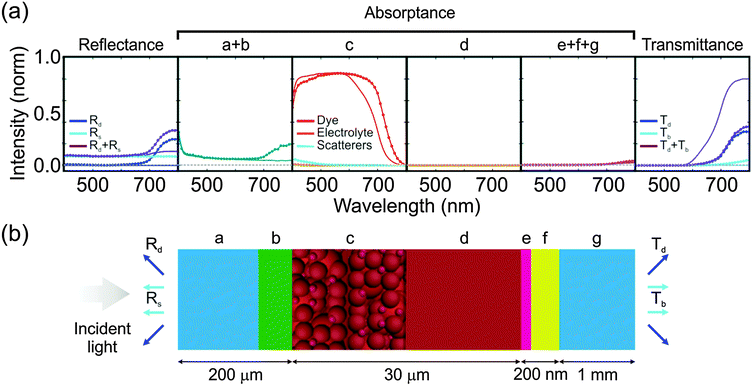 |
| | Fig. 3 (a) Theoretical results of reflectance (left panel), absorptance (intermediate panels) and transmittance (right panel) for the same systems as those considered in Fig. 2. Lines correspond to a reference cell without scatterers, and symbols with lines to a cell with 30% scatterers (r = 160 nm). The cell is illuminated from the PEN substrate. Dashed grey line accounts for 0 reflectance, absorptance or transmittance. Diffuse and specular reflectance are labeled as Rd(λ) and Rs(λ), respectively, and diffuse and ballistic transmittance as Td(λ) and Tb(λ), respectively. Each absorptance panel corresponds to each element comprising the cell: [a + b] PEN and ITO substrate, [c] electrode (distinguishing each component, i.e., dye molecules, electrolyte and TiO2 scatterers in the case of the electrode containing light scatterers), [d] electrolyte, and [e + f + g] counter electrode (platinized FTO and glass). (b) Schematic of the multilayer DSC containing light scatterers, displaying corresponding slab thicknesses. | |
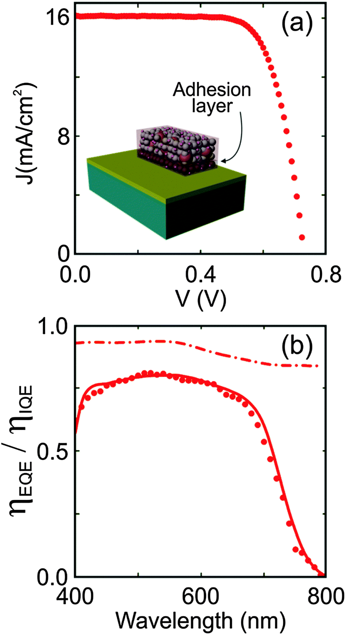
Analysis of these first samples show that light harvesting absorption within the cell is close to optimum after introducing scattering centers in the electrode, while charge collection is still insufficient. This was confirmed by building a much thicker photoanode with an approximate 11.3 micron thick mesoporous titania film, with and without scatterers (Fig. S6 in the ESI†). The cell with scatterers yielded only 7.23% PCE (Table 1), which implies a weak improvement with respect to the cell made with an approximate 8.5 micron thick electrode with the same internal structure (7.1% PCE), in spite of being around 50% thicker. In order to further raise electron collection, we opted for improving the electrical contact between the scatterer embedded nanocrystalline electrode and the ITO. To this aim, a structured electrode consisting of a thinner 2.65 ± 0.15 micron intermediate layer, which we will refer to as “adhesion layer” from here onwards, made with the basic nanoglued titania but without scatterers, was deposited onto the ITO before coating it with a highly diffusive 9.15 ± 0.65 micron thick electrode containing light scatterers (filling fraction of 30%, and r = 160 nm). This approach was suggested by the observation that the electrodes containing light scatterers presented a slightly higher probability of delamination than scatterer free pastes, indicating that the former might not be properly adhered to the substrate and hence having potentially a poorer electrical contact. In Fig. 4a and b, the experimental J–V curves and ηEQE(λ), attained for the adhesion improved electrodes, are displayed with red circles, respectively. In this case, the PCE is 8.55%, which, as far as we know, is the highest reported for a cell containing a photoanode deposited on a plastic substrate. Interestingly, the estimated ηLH(λ) is basically the same as it was before including the intermediate adhesion layer, while the estimated effective electron diffusion length is doubled (Le = 16 microns) and the ηIQE(λ) is significantly higher, being now a few points above 90% for λ < 600 nm and above 85% for longer wavelengths. Direct comparison of ηLH(λ) between cells containing electrodes of ∼8 micron and ∼11 micron total electrode thickness, with and without scatterers and with and without adhesion layer are shown in Fig. S6 in the ESI.† Also in that figure, the optical absorption profiles of cells with scatterers, with and without the adhesion layer, are displayed, presenting identical light absorptance between pairs of comparable systems. Thus, the PCE enhancement observed should be attributed to the improved electron collection derived from the presence of the adhesion layer.
 |
| | Fig. 4 (a) Experimental J–V curve for a plastic cell with a total structured electrode thickness of (11.80 ± 0.50) microns consisting of a first (2.65 ± 0.15) micron adhesion layer without scatterers, and a second layer on top with 30% of nanoparticles of radius 160 nm. The schematics in the inset represent the considered electrode. (b) Experimental (symbols) and theoretical (solid lines) ηEQE(λ) spectra for the same system as that in panel (a). The effective electron diffusion length estimated from the fitting is Le = 16 microns. Corresponding calculated ηIQE(λ) curves are displayed with dashed lines. | |
Table 1 Photovoltaic characterization of cells with various anode and cell structures. “rigid” indicates that the counter electrode is made of a rigid Pt/FTO/Glass arrangement while the counter electrode for “flexible” is Pt/ITO/PEN. “SL” stands for single layer, without an adhesion layer, and “BL” for bilayer in which the anode structure employs an adhesion layer which contains no scattering particles. The substrate for the anode is the flexible ITO/PEN for all cases. The active area of dye-adsorbed TiO2 films was about 0.4 cm2
| Sample |
J SC (mA cm−2) |
V OC (V) |
FF |
PCE (%) |
d (μm) |
Area (cm2) |
| SL-without scatterers-rigid |
12.25 |
0.681 |
0.712 |
5.94 |
8.60 ± 0.05 |
0.387 |
| SL-with scatterers-rigid |
13.61 |
0.704 |
0.741 |
7.10 |
8.60 ± 0.05 |
0.409 |
| SL-with scatterers-rigid |
14.06 |
0.697 |
0.737 |
7.23 |
11.80 ± 0.50 |
0.432 |
| BL-with scatterers-rigid |
16.11 |
0.729 |
0.728 |
8.55 |
11.80 ± 0.50 |
0.390 |
| BL-with scatterers-flexible |
15.94 |
0.719 |
0.679 |
7.79 |
11.80 ± 0.50 |
0.350 |
Once both light harvesting and electron collection were optimized for a cell containing a plastic substrate based photoanode, a fully flexible version of the cell was built by substituting the FTO coated glass, employed as a counter-electrode during the optimization process, by a platinized ITO coated PEN substrate. Comparison of the theoretical parasitic and productive absorptance of the optimized cell employing either a flexible or rigid counter electrode is shown in Fig. S7 and S8 in the ESI,† respectively. The results of the photovoltaic characterization of one of these cells are shown in Fig. 5, together with a scheme of the cell and a photograph of the bendable device. In Table 1, the relevant photovoltaic parameters are listed for all the different cells built during the optimization process. The optimum flexible cell displayed a PCE of 7.79% and, importantly, a short circuit photocurrent of JSC = 15.94 mA cm−2, which is, to the best of our knowledge, the highest reported so far for a flexible DSC, being even above that attained for flexible cells of record efficiency (15.2 mA cm−2).12 Further enhancement of the PCE could be achieved by increasing the fill factor which, as it can be seen in Table 1, drops by an 8% with respect to the optimized cell built using FTO-glass for the counter electrode. This is likely caused by the poorer catalytic activity of the plastic based counter-electrode, as it has been demonstrated elsewhere.34 Most importantly, the ηEQE(λ) of the flexible device remains almost unaltered with respect to that of the optimized rigid device. Overall, these cells consistently show PCE values above 7.5%. For better comparison, Fig. S9 in the ESI,† displays ηIQE(λ) for all cells herein considered. Starting from the reference cell, the first improvement of the internal quantum efficiency observed at short wavelengths when light scatterers are considered is linked to light absorption occurring closer to the contact, as demonstrated by electron generation functions in Fig. 2e and f. The abrupt enhancement of average 10% retrieved when the adhesion layer is incorporated in the structured electrode accounts for an improvement of the electron collection, as confirmed by the enlargement of the electron diffusion length while light harvesting remains almost unaltered.
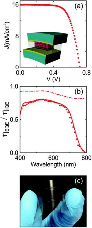 |
| | Fig. 5 (a) Experimental J–V curve for a flexible cell with a total structured electrode thickness of (11.80 ± 0.50) microns consisting of a first (2.65 ± 0.15) micron layer without scatterers, and a second layer on top with 30% of light scatterers (r = 160 nm). (b) Experimental (symbols) and theoretical (solid lines) ηEQE(λ) spectra for the same system as that considered in panel (a). The effective electron diffusion length estimated from the fitting is Le = 16 microns. Corresponding calculated ηIQE(λ) curves are displayed with dashed lines. (c) Image of the fabricated flexible dye solar cell. | |
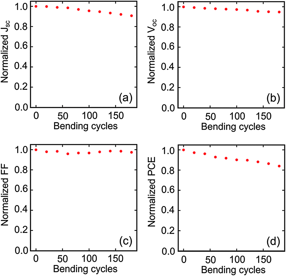
The mechanical stability of the optimized flexible DSC was also investigated by a repeated bending test using a cylindrical rod of radius 15 mm. The photovoltaic properties were recorded before and after various bending cycles. Fig. 6 shows the normalized photovoltaic characterization (JSC, VOC, FF, and PCE) of the designed flexible DSC analysed in Fig. 5. These results demonstrate that this device presents an excellent tolerance to bending tests, reserving all photovoltaic properties after 150 bending cycles, after which the cell performance becomes slightly worse, its JSC decreasing by 10% and its PCE by 15%. The origin of this lowering of JSC and VOC may be attributed to the presence of microcracks generated within the inorganic titania electrode as a consequence of the repeated bendings. As the FF mainly accounts for the electrical conductivity of the thin ITO layer, which shows a better mechanical stability than the thick TiO2 layer, its value remains constant after several bending cycles.23
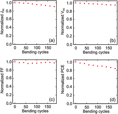 |
| | Fig. 6 Normalized photonic characterization (JSC in panel (a), VOC in panel (b), FF in panel (c) and PCE in panel (d)) of the optimized flexible cell in Fig. 5 as a function of bending cycles with radius 15 mm. | |
Conclusion
In summary, we have presented a combined theoretical and experimental optimization procedure to build highly efficient dye solar cells on plastic substrates with maximized light harvesting and charge collection efficiencies, which are attained following the guidelines of a rigorous and complete optical and electrical model of the cell. The optimized design includes a dispersion of scatterers to reinforce light absorption over the whole spectral range at which the dye absorbs (leading to saturation absorption), and structuring of the electrode incorporating an adhesion layer to enhance charge collection. A synthetic route to prepare these electrodes at low temperatures based on a combination of chemical and physical sintering is employed. An analysis of the effect of introducing gradual changes in the electrode structure have allowed us to rationalize the importance of each variable and quantify its relevance. We have demonstrated that by using this approach it is possible to build DSCs on plastic electrodes with record PCE as high as 8.55%, and fully flexible DSCs with efficiencies as high as 7.79%. In the latter case, the photocurrent reaches a value of 15.94 mA cm−2, above the highest value previously reported for a flexible DSC device (15.2 mA cm−2).12 Moreover, bending tests prove that the optimized design of flexible DSCs is mechanically stable, photovoltaic performance being preserved after 150 bending cycles. We foresee our work may have an impact in the fields of building integrating photovoltaics and in that of rechargeable portable devices, for which light weight and adaptability of energy suppliers are key aspects.
Acknowledgements
Financial support from the European Research Council under the European Union's Seventh Framework Programme (FP7/2007–2013)/ERC grant agreement no. 307081 (POLIGHT) and the Spanish Ministry of Economy and Competitiveness under grant MAT2014-54852-R is gratefully acknowledged. YL acknowledges the financial support from the People Programme (Marie Curie Actions) of the European Union’s Seventh Framework Programme FP7/2007–2013/ under REA grant agreement no. 622533. AJS thanks Spanish Ministry of Economy and Competitiveness for funding through an FPI program under the project MAT2011–23593. MJK acknowledges funding support from the Global Frontier R&D Program on Center for Multiscale Energy System (2012M3A6A7054856), the Technology Development Program to Solve Climate Changes (2015M1A2A2056824) and 2015 University-Institute cooperation program funded by the National Research Foundation under the Ministry of Science, ICT & Future Planning, Korea. This work was also supported by the KIST institutional programs.
Notes and references
- M. Pagliaro, G. Palmisano and R. Ciriminna, Flexible Solar Cells, Wiley-VCH Verlag GmbH & Co. KGaA, Weinheim, 2008 Search PubMed.
- J. Jean, P. R. Brown, R. L. Jaffe, T. Buonnassisi and V. Bulovic, Energy Environ. Sci., 2015, 8, 1200–1219 CAS.
- F. C. Krebs, S. A. Gevorgyan and J. Alstrup, J. Mater. Chem., 2009, 19, 5442–5451 RSC.
- Z. Fan, H. Razavi, J.-W. Do, A. Moriwaki, O. Ergen, Y.-L. Chueh, P. W. Leu, J. C. Ho, T. Takahashi, L. A. Reichertz, S. Neale, K. Yu, M. Wu, J. W. Ager and A. Javey, Nat. Mater., 2009, 8, 648–653 CrossRef CAS PubMed.
- B. Kippelen and J.-L. Brédas, Energy Environ. Sci., 2009, 2, 251–261 CAS.
- I. J. Kramer, G. Moreno-Bautistal, J. C. Minor, D. Kopilovic and E. H. Sargent, Appl. Phys. Lett., 2014, 105, 163902 CrossRef.
- B. J. Kim, D. H. Kim, Y.-Y. Lee, H.-W. Shin, G. S. Han, J. S. Hong, K. Mahmood, T. K. Ahn, Y.-C. Joo, K. S. Hong, N.-G. Park, S. Lee and H. S. Jung, Energy Environ. Sci., 2015, 8, 916–921 CAS.
- A. Chirilă, S. Buecheler, F. Pianezzi, P. Bloesch, C. Gretener, A. R. Uhl, C. Fella, L. Kranz, J. Perrenoud, S. Seyrling, R. Verma, S. Nishiwaki, Y. E. Romanyuk, G. Bilger and A. N. Tiwari, Nat. Mater., 2011, 10, 857–861 CrossRef PubMed.
- S.-M. Lee, R. Biswas, W. Li, D. Kang, L. Chan and J. Yoon, ACS Nano, 2014, 8, 10507–10516 CrossRef CAS PubMed.
- W. Guo, X. Zhang, R. Yu, M. Que, Z. Zhang, Z. Wang, Q. Hua, C. Wang, Z. L. Wang and C. P. Pan, Adv. Energy Mater., 2015, 5, 1500141 Search PubMed.
- S. Ito, N.-L. C. Ha, G. Rothenberger, P. Liska, P. Comte, S. M. Zakeeruddin, P. Pechy, M. K. Nazeeruddin and M. Gräetzel, Chem. Commun., 2006, 4004–4006 RSC.
- H. Arakawa, T. Yamaguchi, T. Sutou, Y. Koishi, N. Tobe, D. Matsumoto and T. Nagai, Curr. Appl. Phys., 2010, 10, S157–S160 CrossRef.
- T. Yamaguchi, N. Tobe, D. Matsumoto, T. Nagai and H. Arakawa, Sol. Energy Mater. Sol. Cells, 2010, 94, 812–816 CrossRef CAS.
- K. Miettunen, J. Halme and P. Lund, Wiley Interdiscip. Rev.: Energy Environ., 2013, 2, 104–120 CrossRef CAS.
- A. Yella, H. W. Lee, H. N. Tsao, C. Y. Yi, A. K. Chandiran, M. K. Nazeeruddin, E. W-G. Diau, C.-Y. Yeh, S. M. Zakeeruddin and M. Grätzel, Science, 2011, 334, 1203 CrossRef CAS PubMed.
- Y. Li, W. Lee, D. K. Lee, K. Kim, N. G. Park and M. J. Ko, Appl. Phys. Lett., 2011, 98, 103301 CrossRef.
- K. Yoo, J.-Y. Kim, J. A. Lee, J. S. Kim, D.-K. Lee, K. Kim, J. Y. Kim, B. Kim, H. Kim, W. M. Kim, J. H. Kim and M. J. Ko, ACS Nano, 2015, 9, 3760–3771 CrossRef CAS PubMed.
- F. E. Gálvez, E. Kemppainen, H. Míguez and J. Halme, J. Phys. Chem. C, 2012, 116, 11426–11433 Search PubMed.
- S. Ito, S. M. Zakeeruddin, R. Humphry-Baker, P. Liska, R. Charvet, P. Comte, M. K. Nazeeruddin, P. Pechy, M. Takata, H. Miura, S. Uchida and M. Grätzel, Adv. Mater., 2006, 18, 1202 CrossRef CAS.
- S. Södergren, A. Hagfeldt, J. Olsson and S. E. Lindquist, J. Phys. Chem., 1994, 98, 5552–5556 CrossRef.
- A. Zaban, S. Ferrere, J. Sprague and B. A. Gregg, J. Phys. Chem. B, 1997, 101, 55–57 CrossRef CAS.
- Y. Li, K. Yoo, D.-K. Lee, J. Y. Kim, H. J. Son, J. H. Kim, C.-H. Lee, H. Míguez and M. J. Ko, RSC Adv., 2015, 5, 76795–76803 RSC.
- Y. Li, D.-K. Lee, J. Y. Kim, B. Kim, N.-G. Park, K. Kim, J.-H. Shin, I.-S. Choi and M. J. Ko, Energy Environ. Sci., 2012, 5, 8950–8957 CAS.
- J. M. Miranda-muñoz, S. Carretero-Palacios, A. Jiménez-Solano, Y. Li, G. Lozano and H. Míguez, J. Mater. Chem. A, 2016, 4, 1953–1961 Search PubMed.
- E. Nichelatti, J. Opt. A: Pure Appl. Opt., 2002, 4, 400–403 CrossRef.
- R. Santbergen, H. Tan, M. Zeman and A. H. M. Smets, Opt. Express, 2014, 22, A1023–A1028 CrossRef PubMed.
- M. Anaya, G. Lozano, M. E. Calvo, W. Zhang, M. B. Johnston, H. J. Snaith and H. Míguez, J. Phys. Chem. Lett., 2015, 6, 48–53 CrossRef CAS PubMed.
- I. W. Sudiarta and P. Chylek, J. Opt. Soc. Am. A, 2001, 18, 1275–1278 CrossRef CAS PubMed.
- F. E. Gálvez, P. R. F. Barnes, J. Halme and H. Míguez, Energy Environ. Sci., 2014, 7, 689–697 Search PubMed.
- J. Ferber and J. Luther, Sol. Energy Mater. Sol. Cells, 1998, 54, 265–275 CrossRef CAS.
- A. Usami, Sol. Energy Mater. Sol. Cells, 2000, 64, 73–83 CrossRef CAS.
- G. Rothenberger, P. Comte and M. Grätzel, Sol. Energy Mater. Sol. Cells, 1999, 58, 321–336 CrossRef CAS.
- Y. Li, K. Yoo, D.-K. Lee, J. Y. Kim, H. Kim, B. Kim and M. J. Ko, Nanoscale, 2013, 5, 4711–4719 RSC.
- D. Kuang, J. Brillet, P. Chen, M. Takata, S. Uchida, H. Miura, K. Sumioka, S. M. Zakeeruddin and M. Gräetzel, ACS Nano, 2008, 2, 1113–1116 CrossRef CAS PubMed.
Footnotes |
| † Electronic supplementary information (ESI) available. See DOI: 10.1039/c6ee00424e |
| ‡ These authors contributed equally to this work. |
|
| This journal is © The Royal Society of Chemistry 2016 |
Click here to see how this site uses Cookies. View our privacy policy here. 
 Open Access Article
 This Open Access Article is licensed under a Creative Commons Attribution-Non Commercial 3.0 Unported Licence
 . ñm(λ) spectra of all materials considered in the calculations are available in Fig. S1, ESI.† The trajectory of each individual photon is described by Fresnel coefficients at the interface of two layers, and by scattering Mie theory when photons interact with light scatterers. In this regard, the main novelty we introduced is the consideration of the influence of the external absorbing media on the diffuse dispersion of light described by Mie theory,28 something that was neglected in previously developed approaches in the field.15,29–32 To determine the trajectory of a photon, we calculate the distance l it travels before suffering either an absorption or a scattering event, through: