
 Open Access Article
 This Open Access Article is licensed under a
 Creative Commons Attribution 3.0 Unported Licence
Light trapping in mesoporous solar cells with plasmonic nanostructures
William R.
Erwin
,
Holly F.
Zarick
,
Eric M.
Talbert
and
Rizia
Bardhan
*
Department of Chemical and Biomolecular Engineering, Vanderbilt University, Nashville, TN, USA 37212. E-mail: rizia.bardhan@vanderbilt.edu
First published on 2nd February 2016
Abstract
Plasmon resonances in metal nanostructures have been extensively harnessed for light trapping in mesoporous solar cells (MSCs), including dye-sensitized solar cells (DSSCs) and recently in perovskite solar cells (PSCs). By altering the geometry, dimension, and composition of metal nanostructures, their optical characteristics can be tuned to either overlap with the sensitizer absorption and enhance light harvesting, or absorb light at a wavelength complementary to the sensitizer enabling broadband solar light capture in MSCs. In this comprehensive review, we discuss the mechanisms of plasmonic enhancement in MSCs including far-field coupling of scattered light, near-field coupling of localized electromagnetic fields, hot electron transfer, and plasmon resonant energy transfer. We then summarize the progress in plasmon enhanced DSSCs in the past decade and decouple the impact of metal nanostructure shape, size, composition, and surface coatings on the overall efficiency. Further, we also discuss the recent advances in plasmon-enhanced perovskite solar cells. Distinct from other published reviews, we discuss the significance of femtosecond spectroscopies to probe the fundamental underpinnings of plasmon enhanced phenomena and understand the mechanisms that give rise to energy transfer between metal nanoparticles and solar materials. The review concludes with a discussion on the challenges in plasmonic device fabrication, and the promise of low-loss semiconductor nanocrystals for plasmonic enhancement in MSCs that facilitate light capture in the infrared.
 William R. Erwin | William Erwin is pursuing his PhD in Chemical and Biomolecular Engineering at Vanderbilt University under the supervision of Prof. Rizia Bardhan. He received a BS in Chemical Engineering from the University of Arkansas in 2012, and was awarded the NSF Graduate Research Fellowship in 2013. His research focuses on the interactions of plasmons with third generation solar materials including dye-sensitized solar cells, organic semiconductors and perovskites. |
 Holly F. Zarick | Holly Zarick is a PhD student in the Chemical and Biomolecular Engineering department at Vanderbilt University. She received her Bachelor's degree in Chemical Engineering from the University of New Mexico in 2012. Currently, she is conducting her PhD studies under the supervision of Dr Rizia Bardhan, with a focus on enhancing the performance of dye-sensitized and organometal trihalide perovskite solar cells with the incorporation of shape and composition controlled plasmonic nanostructures, and further studying the impact on electron dynamics in these systems using ultrafast spectroscopies. |
 Eric M. Talbert | Eric Talbert is a graduate student of chemical engineering at Vanderbilt University. He received a BS in Chemical and Biomolecular Engineering from Rice University in 2014, then joined Prof. Rizia Bardhan's group to investigate light interactions with nanoscale materials. Recently, he has focused on studying absorption dynamics and charge transport in perovskite solar cells using ultrafast spectroscopies. |
 Rizia Bardhan | Prof. Rizia Bardhan joined the Chemical and Biomolecular Engineering department at Vanderbilt University in August 2012. Prior to her faculty appointment she received a PhD in Chemistry from Rice University under the supervision of Prof. Naomi Halas. She did her postdoctoral work at the Molecular Foundry in Lawrence Berkeley National Lab in designing nanomaterials for energy storage and conversion. She is a recipient of the Ralph E. Powe junior faculty enhancement award, NSF BRIGE award, and Forbes “Top 30 Under 30: Rising Stars of Science and Innovation” Award. She has over a decade of experience in plasmonics, nanophotonics, and a strong background in mesoporous solar cells and has published >45 highly cited papers in this field. |
Broader contextEmerging photovoltaics, including PSCs and their predecessors, DSSCs, collectively described as mesoporous solar cells (MSCs), have rapidly evolved as a serious contender to traditional crystalline silicon photovoltaics due to the inexpensive materials and low processing costs. However low efficiencies, specifically in thin-film architectures, have remained a major hurdle to commercialization in these classes of MSCs. The past decade has witnessed significant improvements in device performance of MSCs by integrating subwavelength plasmonic nanostructures in the active layer. Metal nanostructures function as a secondary light source to augment the total light trapped within the mesoporous layer, enabling enhanced carrier generation. This consequently decreases the amount of active material required to achieve high efficiency solar conversion. Plasmon-enhanced thin-film MSCs will ultimately enable integration on flexible substrates, resulting in low-cost and high efficiency flexible solar cells compatible with scalable manufacturing routes such as inkjet printing and roll-to-roll processing. By understanding the fundamental mechanisms of plasmonic enhancement in MSCs, this technology will ultimately enable rapid advancements in the active light management of a range of optoelectronic devices including photovoltaics, sensors, photoelectrochemical cells, and photodetectors. |
1. Introduction
Mesoporous solar cells (MSCs), including dye-sensitized solar cells (DSSCs) and perovskite solar cells (PSCs), form an important class of third generation solar cells or “emerging photovoltaics (PVs)”.1 MSCs are typically composed of a nanocrystalline anatase TiO2 active layer decorated with a monolayer of a sensitizer and coupled with a compact TiO2 electron transport layer. For shuttling holes, either a liquid electrolyte such as I−/I3− redox couple, or a solid-state hole-transport material (HTM) such as Spiro-OMeTAD (2,2′,7,7′-tetrakis-(N,N-di-4-methoxyphenylamino)-9,9′-spirobifluorene) is used.2–4 In the case of DSSCs, ruthenium-based dyes and porphyrins are typically employed as sensitizers,5–9 whereas for PSCs methyl ammonium lead halide (MAPbX3, X = I, Br, Cl) perovskites are the most commonly used light absorbers.3,4,10–15 MSCs have attracted significant attention in the past decade with the promise to lower the cost of solar power by combining the advantages of inexpensive material constituents with solution-processable, scalable, and reproducible device fabrication. This has resulted in tremendous research efforts to improve their efficiency and stability, and MSCs are already being commercialized (G24, Sony, Aisin Seiki) for niche markets to power consumer electronics and low-power technologies.16,17 However, to adopt these emerging PVs globally for high-power applications and utility-scale power generation, efficiencies greater than 20% are necessary.Subwavelength metal nanostructures have been demonstrated as a highly effective route to augment light harvesting in solar devices, giving rise to improved optical absorption, carrier generation, and overall power conversion efficiency.18–20 The past decade has witnessed a significant rise in plasmonic enhancement of MSCs with Au, Ag, and Au/Ag bimetallic nanostructures resulting in 20–60% improvement in efficiency.21–30Fig. 1a shows a schematic of metal nanostructures integrated in MSCs. Following photoexcitation in metal nanostructures incident photons are coupled to conduction band electrons, giving rise to collective oscillations of the electrons defined as localized surface plasmon resonances (LSPRs).31–34 By engineering the geometry, dimension, and composition, the LSPR of metal nanostructures can be manipulated to capture specific wavelengths of solar light to supplement or complement the absorption by the sensitizer. This ultimately increases the total light trapped within the mesoporous layer of MSCs (Fig. 1b–f).35–39 In this review, we highlight the fundamental mechanisms that contribute to plasmonic enhancement in MSCs, followed by a summary of the progress in metal-enhanced DSSCs and PSCs in the past decade. Further, we discuss the challenges in the fabrication of metal nanostructure integrated devices and summarize the importance of femtosecond time-resolved spectroscopies to understand the foundational principles of plasmon-enhanced phenomena. The review concludes with a discussion of the potential of new plasmonic materials beyond Au and Ag nanostructures and a brief outlook on future directions in plasmonic enhancement in PSCs, both in the mesoscopic and planar architectures.
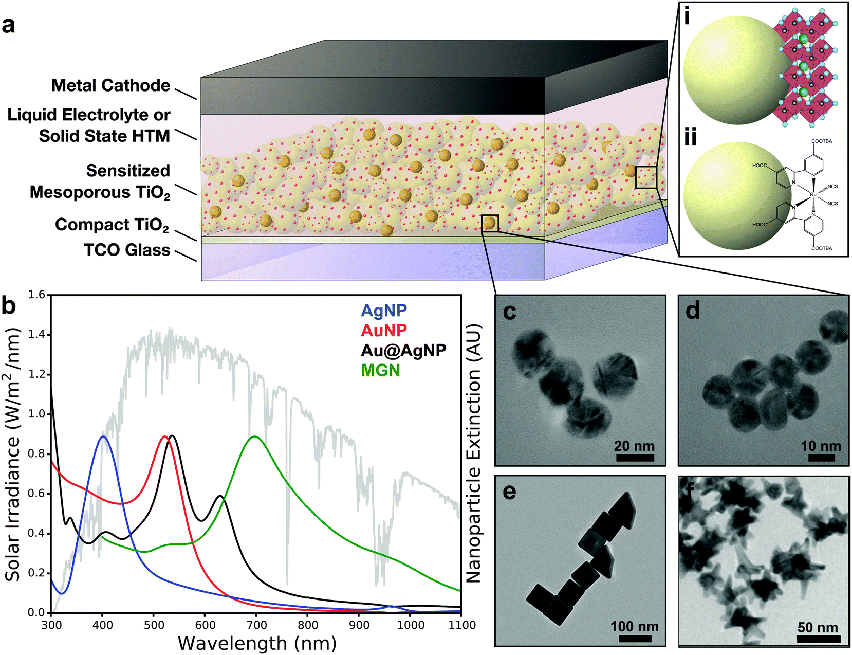 | ||
| Fig. 1 (a) Generalized mesoporous solar cell schematic for (i) perovskite solar cells and (ii) dye-sensitized solar cells. (b) Solar irradiance overlaid with extinction spectra of nanostructures corresponding to TEM images of (c) Ag nanoparticles (Ag NP), (d) Au nanoparticles (Au NP), (e) Au@Ag nanoparticles (Au@Ag NP), and (f) multibranched gold nanoantennas (MGN). Panels e and f adapted with permission from ref. 41 and 42, respectively. Copyright 2014 American Chemical Society. | ||
2. Mechanisms of plasmonic enhancement
LSPRs in metal nanostructures give rise to a collection of optical and electronic effects, processes that occur during the excitation and subsequent decoherence of a plasmon and ultimately contribute to enhanced photonic effects in MSCs.31–33 Plasmonic enhancement in solar devices is attributed to (i) radiative effects, in which the LSPR relaxes and re-radiates light into the absorptive layer or the metal nanostructures act as a secondary light source that enhances local electric fields, and (ii) non-radiative effects where the LSPR relaxes and energy is subsequently transferred to vicinal semiconductor, enhancing the current generation.18–20,40 Metal nanostructures essentially act as a direct sensitizer during non-radiative processes. This section will explain the four mechanisms of plasmonic enhancement, shown in Fig. 2, including light scattering and electromagnetic fields categorized within radiative effects, and hot electron transfer and plasmon resonant energy transfer which fall under non-radiative effects.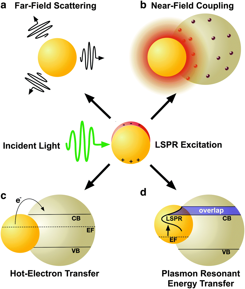 | ||
| Fig. 2 Schematic illustration of plasmon enhancement mechanisms of radiative effects (a) far-field scattering and (b) near-field coupling; and nonradiative effects: (c) hot-electron transfer, and (d) plasmon resonant energy transfer. | ||
2.1 Radiative effects
LSPRs of metal nanostructures have finite lifetimes following which they decay either radiatively by emitting a photon, or nonradiatively by generating electron–hole pairs.31–33 The radiative decay process either gives rise to electromagnetic fields in the nanostructures' “near-field” or light scattering into the nanostructures' “far-field.” Radiative effects are best understood as a dipole–dipole coupling between the metal nanoparticle dipolar fields with the molecule or sensitizer dipole. The metal-molecule radiative coupling is proportional to r−3, where r is the distance from the molecule to the nanostructure. At the plasmon resonance however, radiative fields follow r−6 dependence and may far exceed unity.43–47 In this section, we discuss the basic concepts and mechanisms of plasmonic enhancement in MSCs by radiative processes.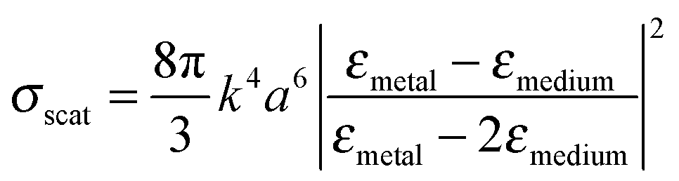 | (1) |
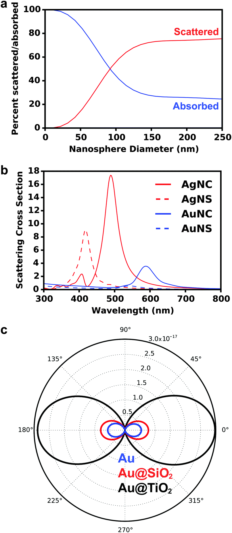 | ||
| Fig. 3 (a) Percent of light scattered and absorbed calculated as a function of Au nanosphere diameter integrated from 300–800 nm. (b) Calculated scattering cross sections of 50 nm Au and Ag nanospheres (NS) and nanocubes (NC) indicate that both shape and composition control nanoparticle albedo. (c) Calculated angular scattering of 50 nm Au nanosphere bare, with a 10 nm SiO2 coating, and with a 10 nm TiO2 coating. All calculations were performed in Lumerical FDTD Solutions. | ||
At the crossover size of ∼90 nm for spherical Au nanoparticles, the amount of light absorbed and scattered is equivalent, indicating nanoparticle size can be tuned to achieve desired absorptive and scattering properties for maximum solar harvesting.
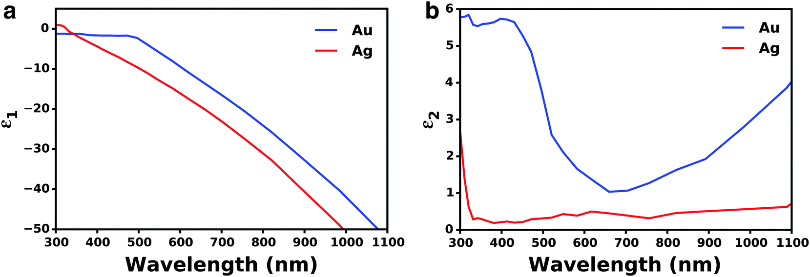
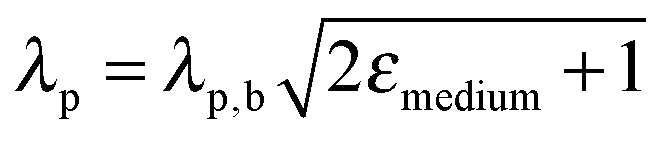
Beyond the size of metal nanostructures, shape also controls the far-field scattered light attributed to the enhanced polarizability, or ability to polarize incoming light, of the nanostructures (Fig. 3b).35,58–60 The effect of polarizability is particularly dominant for non-spherical nanostructures with sharp edges and corner such as cubes, pyramids, and octahedrons, as well as layered concentric nanostructures where the polarizability is enhanced at the metal/dielectric interface of each layer.61 Further, light scattering characteristics are affected by the composition of nanostructures, where Ag has stronger radiative properties due to less Ohmic losses than Au (Fig. 3b). This is best described by the complex dielectric functions of bulk Ag and Au, which consists of a real (Fig. 4a) and imaginary (Fig. 4b) part. The real part of the dielectric function (ε1) determines the polarization response and scales with carrier concentration in the metal. The imaginary part of the dielectric function (ε2) determines the optical losses including interband and intraband losses. For Au, intraband or Drude losses, are high in the near-infrared and lower in the visible. Alternatively, interband losses in Au are high at shorter wavelengths. The smaller imaginary dielectric function of Ag across all wavelengths implies lower optical losses (i.e. plasmon damping), which results in higher scattering efficiency and narrower plasmon linewidths.62–65 This fundamental difference in the optical behavior of Au and Ag has been extensively harnessed in plasmonic sensing, and more recently applied to MSCs where Ag has shown stronger enhancement in carrier generation.21,38,66–72 Section 3 of this review will discuss the impact of nanostructure size, shape, and composition on DSSCs and PSCs in more detail.
 | ||
| Fig. 4 (a) Real part of the dielectric function for Au and Ag. (b) Imaginary part of the dielectric function of Au and Ag. Data adapted from ref. 63. | ||
Finally, far-field effects in MSCs may be tuned as a function of the permittivity of the medium (εmedium) surrounding the metal nanostructures.73–76 A higher εmedium (i) red-shifts the LSPR frequency enabling capture of solar photons where the sensitizer poorly absorbs, and (ii) enables preferential scattering in targeted directions.77 Calculated angular scattering (Fig. 3c) of 50 nm Au nanoparticles uncoated, and coated with 10 nm SiO2 and TiO2 demonstrates >3× light scattering for TiO2 coated nanoparticles. The dielectric constant of TiO2 is ∼6.8 whereas that of SiO2 is ∼2.1. The red-shift in LSPR frequency, λp, with increase in εmedium is best understood by the Drude approximation for quasi-static metal nanoparticles, given by:
 | (2) |
 | (3) |
 | ||
| Fig. 5 Energy diagram of a plasmon-enhanced DSSC system detailing how coupling between the plasmonic nanostructure and N719 dye results in enhanced absorption, thereby increasing the electron transfer from the sensitizer to the mesoporous TiO2. Figure adapted with permission from ref. 78. Copyright 2014 American Chemical Society. | ||
Electromagnetic near-fields at the plasmon resonance decay proportional to r−6, where r is the distance from the nanostructure, and typically extend <50 nm from the nanostructure surface (Fig. 6a). Analogous to far-field scattering, the near-fields generated by the LSPR are governed by the metal nanostructure morphology and composition.57,59,60 Non-spherical nanostructures with sharp features, such as nanocubes, generate a high concentration of charges localized at the edges and corners, attributed to the lightning-rod effect.80–83 Finite difference time domain (FDTD) simulations demonstrate the impact of nanostructure morphology and composition on the local electromagnetic field intensities at the plasmon resonance (Fig. 6b–e). These intense fields in nanocubes decay slower and extend much farther than their spherical counterparts (Fig. 6b–e). The lightning-rod effect was first reported by Gersten and Nitzan,84 and then by Liao and Wokaun85 to describe the fields localized at the tips of prolate ellipsoids. Liao et al. defined the lightning-rod factor, γ, given by:
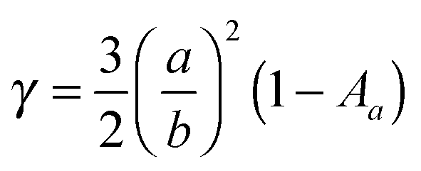 | (4) |
![[thin space (1/6-em)]](https://www.rsc.org/images/entities/char_2009.gif) :1 γ = 12, and for an ellipsoid with aspect ratio 4:1 γ = 22. The lightning rod effect can be extended to other anisotropic shapes and ultimately explains the higher efficiencies observed when MSCs are integrated with non-spherical nanostructures. Near-field effects are also stronger for Ag relative to Au (Fig. 6a) due to the wavelength-dependent behavior of the real and imaginary dielectric functions of the metals as described in Section 2.1.1 and shown in Fig. 4. We note that a limitation of radiative enhancements is that photon energy is unchanged when scattered, so only light that is within the band gap of the semiconductor is utilized.
:1 γ = 12, and for an ellipsoid with aspect ratio 4:1 γ = 22. The lightning rod effect can be extended to other anisotropic shapes and ultimately explains the higher efficiencies observed when MSCs are integrated with non-spherical nanostructures. Near-field effects are also stronger for Ag relative to Au (Fig. 6a) due to the wavelength-dependent behavior of the real and imaginary dielectric functions of the metals as described in Section 2.1.1 and shown in Fig. 4. We note that a limitation of radiative enhancements is that photon energy is unchanged when scattered, so only light that is within the band gap of the semiconductor is utilized.
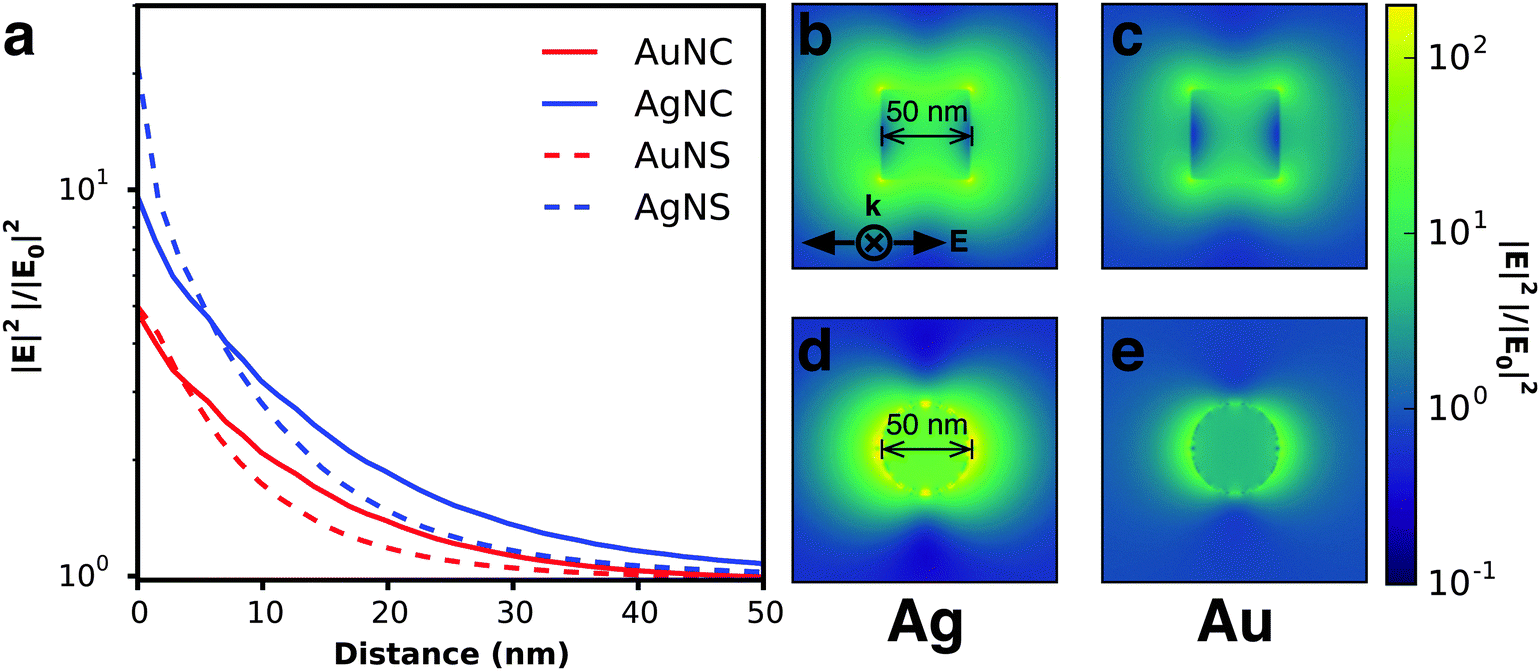 | ||
| Fig. 6 (a) Calculated near field enhancement as a function of distance from the particle surface averaged over the 300–800 nm spectral range; values are averaged over the x, y, and z planes intersecting the particle. Near field profiles at peak plasmon resonance for (b) Ag nanocube at 490 nm, (c) Au nanocube at 580 nm, (d) Ag nanosphere at 420 nm, and (e) Au nanosphere at 530 nm are shown. All calculations performed in Lumerical FDTD Solutions. | ||
2.2 Non-radiative effects
While radiative effects are the dominant mechanism for plasmonic enhancement in MSCs, non-radiative effects also play a significant role and facilitate coupling of below band gap energy into the semiconductor. Therefore by effectively harnessing non-radiative enhancement processes, ultra-high efficiencies may be realized in single junction solar cells. Two distinct non-radiative effects contribute to enhanced carrier generation in MSCs: hot-electron transfer (HET), and plasmon resonant energy transfer (PRET). Both of these non-radiative energy transfer processes have been studied in photodetectors86 and solar photocatalysis,87,88 but remain poorly understood in MSCs. In this section, we discuss the fundamentals of non-radiative enhancement in MSCs with plasmonic nanostructures.As shown in Fig. 7, prior to relaxation, hot electrons can be efficiently captured by forming a Schottky barrier, ΦSB, with a semiconductor such as TiO2, which has a high density of states in its conduction band and permits rapid electron injection over ΦSB. Hot electrons with sufficient energy to overcome the ΦSB can be injected into the semiconductor conduction band.86,100–105 Since the energy needed for HET is smaller than the bandgap, Eg, of the semiconductor, spectral overlap between the metal nanostructure and semiconductor is not required in order for energy transfer to occur. However, HET can only occur when the Fermi levels of the metal and semiconductor are equilibrated, and there is a clear path for electrons to travel between the two.86,93 In most plasmon enhanced DSSC systems, metal nanoparticles are coated in an insulating interlayer such as SiO2. For HET to occur, the layer must be thinner than the electron tunneling barrier of the material, which is 3 nm for SiO2.106 Despite the promise of HET in enhancing carrier generation in plasmon enhanced MSCs, recombination of the carriers at interfaces and defect sites remains a challenge. Further, relaxation of hot holes before reaching the hole-transport material, which shuttles the holes to the counter electrode in solar cells, remains a major barrier to successful implementation of HET in MSCs.
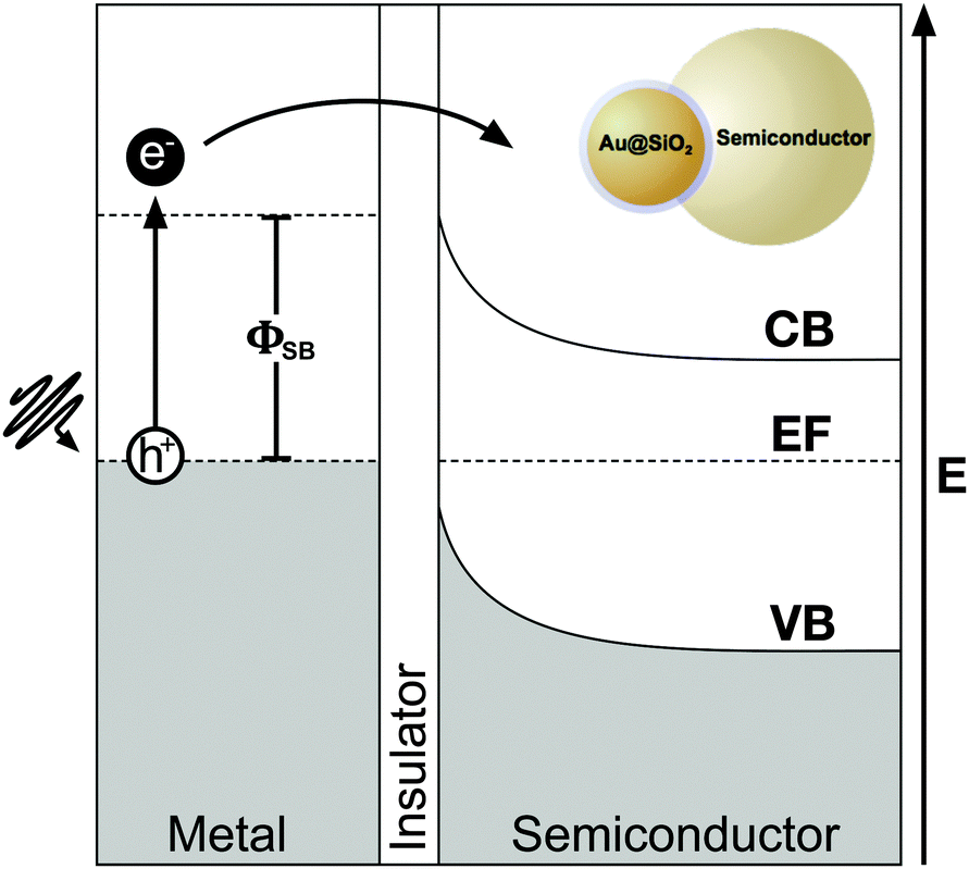 | ||
| Fig. 7 Schematic energy diagram of the hot electron transfer process: first, the excitation and subsequent decoherence of a plasmon produces hot electrons and holes, followed by diffusion of hot electrons to the metal–semiconductor interface. Next, hot electrons with sufficient energy traverse the Schottky barrier and tunnel through a thin insulator (≤2 nm) to enter the conduction band of the neighboring semiconductor. | ||
The efficient generation and capture of hot electrons is determined by the shape, size, and composition of metal nanostructures, as well as device design. Nordlander and co-workers recently calculated hot electron generation in Ag nanoparticles of 15 nm and 25 nm diameter.93 They demonstrated that when hot carriers are generated with energies close to the Fermi level, an increase in hot carrier production occurs with increasing size. However, larger nanoparticles produce less energetic carriers than smaller Ag nanoparticles. Their analysis also revealed the spatial distribution of hot electrons is primarily localized along the direction parallel to the polarization of the incident field. Govorov and co-workers confirmed that hot electrons are most efficiently generated in Au or Ag nanostructures <20 nm size. Since the mean free path of an electron is on the order of 20 nm, hot electrons generated in nanoparticles with dimension >20 nm have energies closer to the Fermi level of the metal, and originate from defects in the nanoparticle.107 The composition of metal nanostructures also determines the rate of Landau damping; for example, metals with strong intraband transitions such as Pd, Pt, and transition metals have weak radiative properties and efficiently convert incident photons to hot electrons.15 Hot electrons can also be preferentially generated in metal nanostructures with a strong subradiant (dark) mode, such as complex layered architectures or highly anisotropic nanostructures. The superradiant or bright modes in such metal nanostructures directly couple to the incident light and are spectrally broadened due to radiative damping, whereas subradiant modes do not couple to light, hence they are spectrally narrow and relax non-radiatively to produce hot electrons. For example, multilayered metal/dielectric nanoshells,61,108 nanostructures with broken symmetry,109–111 and ordered clusters of nanostructures112–114 all have strong subradiant modes and can produce hot electrons.
By engineering the morphology and dimensions of metal nanostructures and coupling with appropriate semiconductors whose ΦSB is relatively close to the Fermi level of the metal, HET can be promoted in MSCs. Challenges remain for large scale implementation of hot electron generating devices, including wet chemical synthesis of geometries which promote HET, and the synthesis of an appropriately thin insulating layer to allow for HET to neighboring semiconductor while minimizing unwanted recombination.
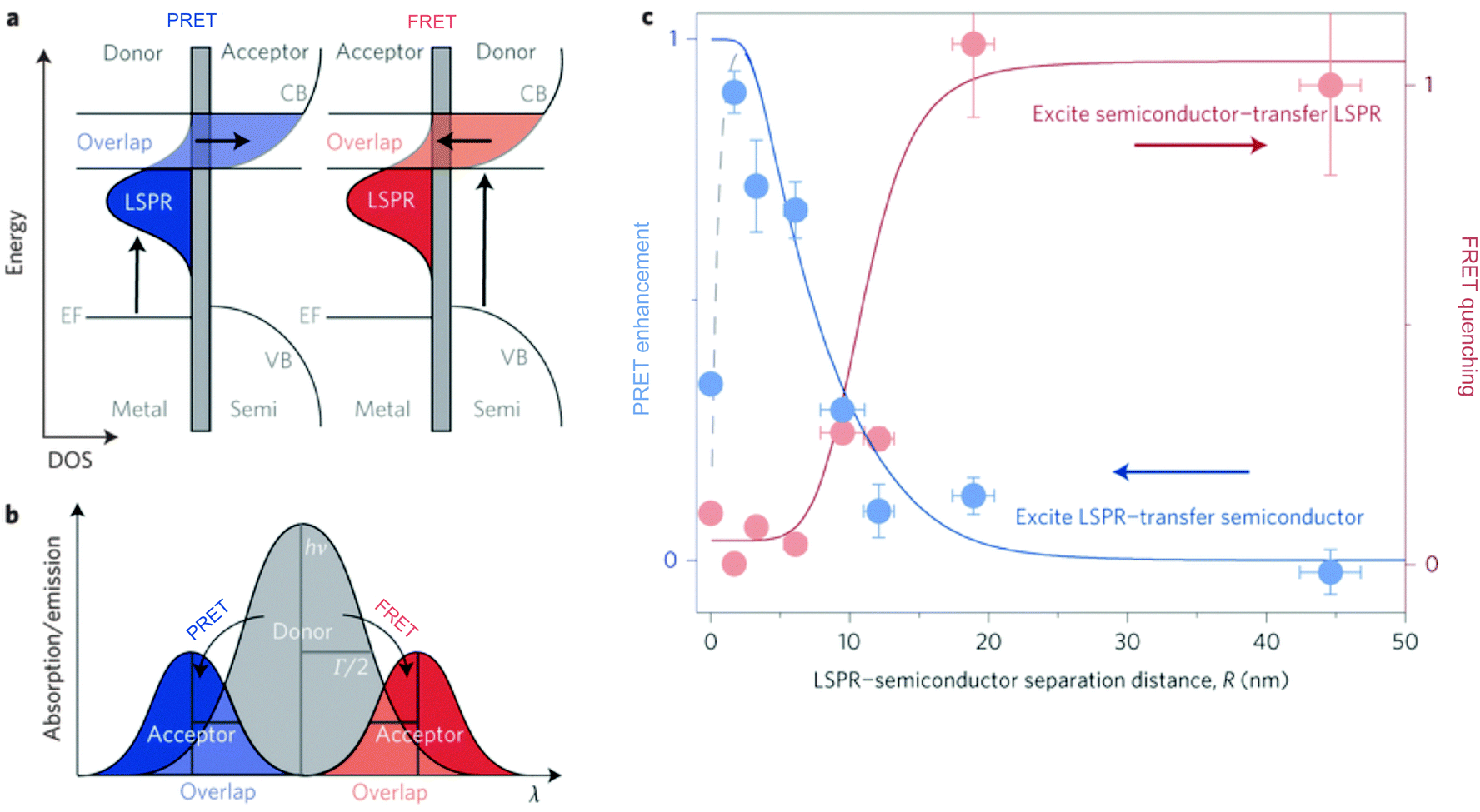 | ||
| Fig. 8 (a) In PRET, energy in the plasmon is transferred to the acceptor molecule, and in the competing process, FRET, energy is transferred from the semiconductor to the plasmon. (b) Diagram distinguishing PRET and FRET spectrally, where PRET results in energy upconversion and FRET results in energy downconversion. (c) The bulk of energy transfer in both the PRET and FRET mechanisms occur within 20 nm of the LSPR. Adapted by permission from Macmillan Publishers Ltd: ref. 87, copyright 2015. | ||
Plasmonic enhancement in solar devices by PRET often competes with FRET, which takes away excited carriers from the semiconductor, and hence distinction of the two processes is essential to preferentially enable PRET. In a recent work, Wu and co-workers differentiated the two processes and demonstrated that in the dipole–dipole coupling regime, exciting the plasmon results in coherent plasmon-to-semiconductor energy transfer via PRET, whereas exciting the semiconductor at its bandgap results in incoherent semiconductor-to-plasmon energy transfer via FRET (Fig. 8b).87 They defined the efficiency of dipole–dipole energy transfer for FRET (EFRET) and PRET (EPRET) as follows:
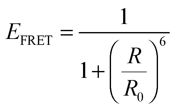 | (5) |
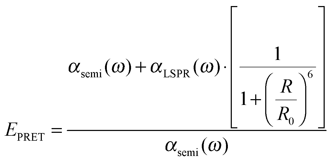 | (6) |
While the evidence of PRET has been shown in solar photochemistry and photocatalysis, the contributions of PRET to enhance light trapping in MSCs remains poorly explored thus far. Since spectral overlap between metal and semiconductor is required for PRET, this mechanism occurs under similar conditions as radiative near field enhancement. Therefore, it is often difficult to differentiate the contributions of the radiative and non-radiative mechanisms. Further work is required to elucidate the potential for PRET in both DSSCs and PSCs.
3. Plasmon enhanced DSSCs
Since the first published report of metal nanostructure-mediated enhancement in dye-sensitized solar cells in 2000, advances in the fabrication of morphology-controlled metal nanostructures, and their subsequent implementation in DSSCs have resulted in significant efficiency enhancements.123 In this section, we discuss the effects of shape, size, and composition of metal nanostructure on their ability to enhance light trapping in DSSCs, while summarizing recent progress in the field.3.1 Influence of nanostructure size on DSSCs performance
The radiative and non-radiative plasmonic properties of metal nanostructures are largely controlled by their dimension, which strongly impacts their light harvesting capability. While nanostructures <90 nm in diameter are strong absorbers, larger nanostructures primarily scatter. The ratio of absorption to scattering as a function of size of Au nanospheres is depicted in Fig. 3a with the crossover point at 90 nm. Particularly in nanospheres, the absorption cross-section scales linearly with volume whereas scattering cross-section scales with the square of the nanosphere volume. At even smaller length scales, when the characteristic size is comparable to the electron mean free path (∼20 nm for Au), these nanostructures display strong surface dispersion and electron–electron scattering.107,124,125 A schematic illustration of the size-dependent enhancement mechanisms in DSSCs is shown in Fig. 9 where an Au nanosphere of variable size is in proximity of a sensitized TiO2 nanoparticle. In the 5 nm size regime (Fig. 9a), where non-radiative effects are dominant, surface dispersion promotes photocharging and hot-electron transfer (HET) from the metal to the semiconductor. At larger sizes radiative effects primarily drive light harvesting in DSSCs. At the 45 nm size regime (Fig. 9b), electromagnetic near-fields strongly contribute to plasmonic enhancement, whereas at 120 nm (Fig. 9c) far-field scattering dominates the increase in photocurrent.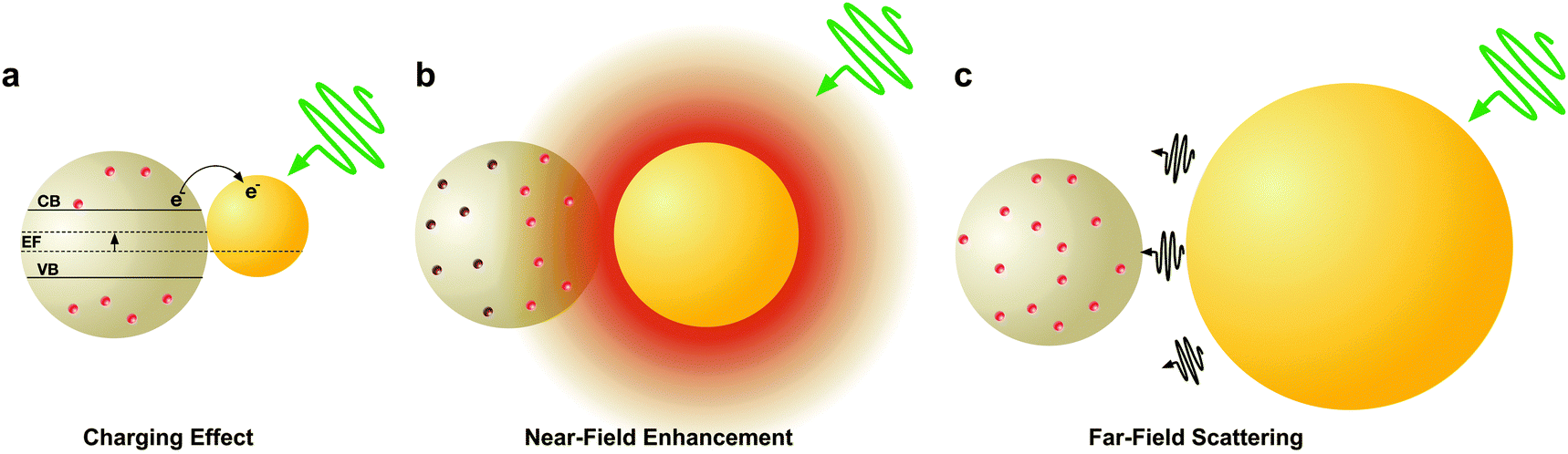 | ||
| Fig. 9 Schematic illustration of the influence of the size of a nanostructure on the corresponding plasmonic enhancement mechanism. (a) The photocharging effect from a ∼5 nm Au nanoparticle. (b) The near-field plasmonic effect from a ∼45 nm Au nanoparticle. (c) Light scattering as a result of a ∼120 nm Au nanoparticle. | ||
Plasmon enhanced light harvesting in DSSCs has been achieved in two different configurations: (i) distribution of the metal nanostructures on top of the TiO2 photoanode, and (ii) integrated within the mesoporous TiO2 layer. In the former configuration, highly scattering >100 nm metal nanostructures are ideal to capture light not absorbed by the sensitizer and backscatter it into the active layer. Enhancement in this configuration is limited to far-field effects since the large separation between the metal/sensitizer and metal/TiO2 limits HET, PRET, and near field enhancements. While enhancement schemes with metal nanostructures on top of the photoanode have been implemented,126,127 the observed photocurrent improvements were comparable to incorporating a TiO2 scattering layer, indicating this configuration does not require a plasmonic nanostructure. In a recent work, however, Taghavinia et al. used finite element method simulations of a nanoparticle/titania system and observed a 40% increase in absorption with 700 nm Ag microparticles relative to a 2% increase with 100 nm Ag nanoparticles.128 This effect was attributed to the ability of the microparticles to divert light at larger angles, increasing the optical path length within the titania layer, thereby coupling light into more guided modes. Kang et al. also recently demonstrated that far field plasmonic enhancement can be achieved by incorporating nanostructures into the electrolyte layer.21 The ∼60 μm thickness of the electrolyte layer allows a larger density of nanostructures to be added, increasing the number of photons that can be scattered. By evaluating a range of diameters of Ag nanospheres from 8–98 nm, they observed a monotonic increase in efficiency with nanoparticle size. Maximum enhancements were achieved with highly scattering 98 nm nanoparticles.
In addition to the distribution of metal nanostructures on top of the photoanode, the best plasmonic enhancements in DSSCs have been achieved by homogeneous integration of nanostructures throughout the mesoporous TiO2 active layer. In this configuration, nanostructures are in close proximity to both the TiO2 and sensitizer molecules, enabling both radiative (near-field and far-field coupling) and non-radiative (PRET, HET) enhancements. Straightforward processing techniques and the versatility of the embedded configuration have enabled this architecture to be thoroughly studied; nanostructures in the range of 5–200 nm have been shown to successfully boost power conversion efficiency in DSSCs.118,129,130 The impact of nanoparticle size in DSSCs has been studied by Wang et al. and Sardana et al., who reported Au nanoparticles in the 30–50 nm range to be optimal for DSSC enhancement.119,131 Incremental improvements in Jsc resulted from the presence of small (<5 nm) nanoparticles, however notable enhancements in Voc were observed and attributed to photocharging effects, suggesting electron storage in ∼5 nm Au nanoparticles shifts the Fermi level of TiO2 to more negative potentials.118 The Fermi level shift results in longer electron lifetimes and higher recombination resistance, ultimately improving charge transport in the electrode, which is reflected in the increased Voc. Medium sized (30–50 nm) Au nanostructures gave rise to the most dramatic improvement in Jsc and incident photon to charge carrier efficiency (IPCE), which is attributable to a combination of radiative and non-radiative effects. Both groups observed efficiency boost with larger nanoparticles (80–110 nm) where far-field scattering dominated other plasmonic enhancement mechanisms; however the champion efficiencies were achieved with 5–50 nm Au particles, although by different mechanisms.
3.2 Influence of nanostructure morphology
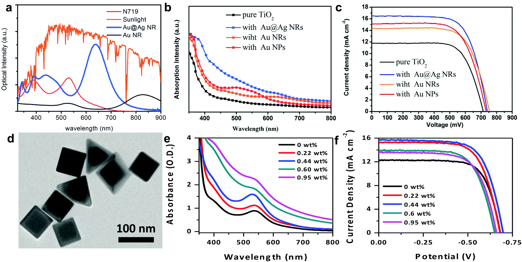
While early studies of plasmonic enhancement in DSSCs were focused primarily on spherical metal nanostructures,23,27,133,134 recently anisotropic morphologies have gained tremendous attention due to their improved absorption and scattering properties, and enhanced spectral tunability.51,66,67,78,130,132,135,136 Plasmonic enhancement in DSSCs has been observed with nanorods,25,66 nanocubes,30 nanoprisms,51,135 and core/shell nanostructures,25,30 among others. Non-spherical nanostructures with varying levels of symmetry give rise to enhanced polarizability. Increased polarizability results in multiple plasmon resonances including dipolar, quadrupolar, and higher order modes, as well as gives rise to red-shifts in the optical resonance.59,137–139 These multiple plasmon modes facilitate spectral overlap and coupling with a range of dye sensitizers. Further, non-spherical nanostructures facilitate a higher concentration of charges localized at the corners and edges giving rise to confined near fields, attributable to the quasi-static lightning-rod effect discussed in Section 2.1.2.39,80,82,84,85 Confined electromagnetic fields can be utilized as a secondary light source to augment absorption by proximal sensitizers.A few examples of shape-controlled nanostructures employed in DSSCs and their respective absorption spectra and IPCEs are displayed in Fig. 10. Snaith and co-workers demonstrated one of the first works on plasmon-enhanced DSSCs with 15 nm spherical Au nanoparticles coated in a ∼3 nm layer of silica (Fig. 10ai) embedded in a 1.1 μm thick mesoporous TiO2 layer. The nanoparticle plasmon resonance at ∼524 nm corresponded well with the Z907 sensitizer and improved the overall absorption of the photoanodes (Fig. 10aii). They observed an increase of 57% in average device performance for plasmon-enhanced devices and an analogous improvement in the IPCE (Fig. 10aiii). They attributed the improvement in the nanoparticle incorporated devices to increased light harvesting as well as an increase in Voc and FF correlating to the photocharging effect observed for small nanostructures discussed previously. Our group demonstrated the use of shape-controlled 45 nm edge-length Au nanocubes coated with a 5 nm silica layer, Au@SiO2 nanocubes (Fig. 10bi). The optical resonance of the Au@SiO2 nanocubes at 545 nm overlaps with the absorption peak of the N719 sensitizer at 530 nm. We performed finite difference time domain (FDTD) simulations showing the nanocube electric fields are localized near the edges and corners (Fig. 10bi-inset). We observed a 34% improvement in power conversion efficiency (PCE) using 1.8 wt% 45 nm Au@SiO2 nanocubes, in agreement with the literature for this size and composition. The enhanced light harvesting by these shape-controlled nanostructures (relative to the spherical nanostructures in Fig. 10ai) is reflected in the IPCE spectra shown in Fig. 10biii. Contrary to the work described by Snaith and co-workers, we attributed the improved device efficiencies by the Au@SiO2 nanocubes to radiative effects, resulting in plasmon-molecular coupling between the nanocubes and N719 dye; this is reflected in the increase in photocurrent with minimal change in Voc or FF.
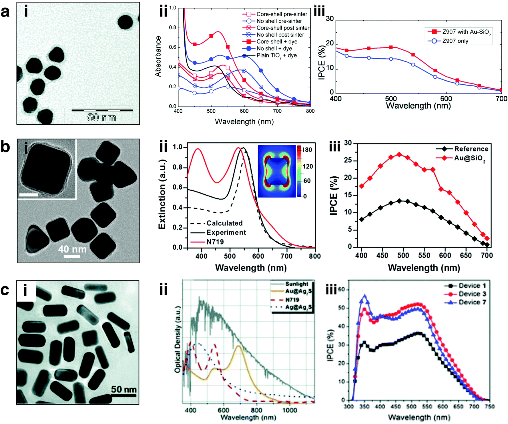 | ||
| Fig. 10 (a) (i) TEM image of Au@SiO2 nanospheres, (ii) absorbance of active layers with and without particle incorporation, (iii) enhanced IPCE over the visible spectrum attributed to presence of Au nanoparticles. Adapted with permission from ref. 22. Copyright American Chemical Society 2011. (b) (i) TEM image of Au@SiO2 nanocubes, (ii) extinction of calculated and experimental Au nanocubes overlaid with N719 absorbance; FDTD electric field profile is provided in the inset, colorbar represents |E2|/|E02|. (iii) IPCE of Au incorporated and control devices. Adapted with permission from ref. 78. Copyright American Chemical Society 2014. (c) (i) TEM of Au nanorods, (ii) extinction of Au@Ag2S nanorods overlaid with N719 dye and solar irradiance, (iii) IPCE of control versus plasmonic devices. Adapted with permission from ref. 132. Copyright American Chemical Society 2012. | ||
While Au nanospheres and nanocubes provide direct spectral overlap with the sensitizers used in DSSCs, modifying the morphology of the nanostructure, anisotropic nanostructures can achieve panchromatic light absorption. Chen et al. demonstrated this concept by using 50 nm Au nanorods (Fig. 10ci) with an aspect ratio of ∼2.2 and an Ag2S protective coating embedded throughout the mesoporous TiO2 active layer.132 Nanorods support two distinct plasmon resonances, a transverse and a longitudinal mode; the longitudinal mode is tunable from the visible to near-IR by altering the aspect ratio of the nanorod. This is evident in Fig. 10cii, where the Au/Ag2S nanorods show a longitudinal resonance at 685 nm enabling broadband solar light capture at wavelengths complimentary to N719 dye sensitizer. The authors observed a ∼38% increase in photocurrent generation in the 600–720 nm region as determined by IPCE (Fig. 10ciii), leading to an overall ∼30% enhancement in PCE by plasmon-enhanced devices.
Beyond the geometries discussed in Fig. 10, we have provided a comprehensive list in Table 1 including a range of shape-controlled metal nanostructures employed in DSSCs in recent literature. The diverse morphologies used for plasmonic enhanced MSCs demonstrate tremendous progress in this field in addition to providing motivation for further understanding of these metal/molecule systems.
| Composition | Passivation layer | Nanostructure | Size (nm) | Reference PCE (%) | Plasmon enhanced (%) | Enhancement (%) | Ref. |
|---|---|---|---|---|---|---|---|
| Ag | EMIm-DCA | Nanosphere | 8–98 | 6.34 | 8.05 | 27 | 21 |
| Au | TiO2 | Nanosphere | 100 | 5.21 | 5.97 | 15 | 228 |
| Au | SiO2 | Nanosphere | 15 | 1.70 | 4.00 | 135 | 22 |
| Au | — | Nanosphere | 15 | 6.52 | 7.70 | 18 | 229 |
| Au | — | Nanosphere | 36 | 6.17 | 7.35 | 19 | 131 |
| Au | — | Nanosphere | 18 | 3.44 | 4.11 | 19 | 229 |
| Au | Ag2S | Nanorod | 40 | 5.80 | 7.10 | 22 | 132 |
| Au | SiO2/TiO2 | Nanoparticle | 5 | 9.29 | 10.21 | 10 | 118 |
| Au | TiO2 | Nanosphere | 20 | 6.03 | 8.46 | 40 | 23 |
| Au/Ag | TiO2 | Nanosphere | 15 | 8.30 | 10.80 | 30 | 133 |
| Ag | — | Nanodome array | 300 | 5.64 | 5.93 | 5 | 157 |
| Ag | SiO2 | Nanoparticle | <5 | 2.70 | 4.00 | 48 | 24 |
| Ag | SiO2 | Nanoparticle | <5 | 6.20 | 8.10 | 31 | 230 |
| Au@Ag | — | Nanorod | 70 | 5.91 | 8.43 | 43 | 25 |
| Ag | TiO2 | Nanowire | 80 nm | 6.16 | 8.84 | 44 | 66 |
| Ag | — | Nanoparticle | <5 | 6.98 | 8.19 | 17 | 151 |
| Au | TiO2 | Nanoparticle | 5 | 6.25 | 8.13 | 30 | 26 |
| Au | SiO2 | Nanoprism | 20–150 | 3.90 | 4.50 | 15 | 51 |
| Ag | SiO2 | Nanoprism | 30 | 6.50 | 8.40 | 29 | 135 |
| SiO2@AuNP | TiO2 | Nanosphere | 200 | 4.51 | 5.74 | 27 | 27 |
| Ag | TiO2 | Nanoparticle | <5 | 7.10 | 8.90 | 25 | 142 |
| Ag | — | Square array | 500 | 4.59 | 5.69 | 24 | 68 |
| Au | DMAP | Nanoparticle | 5 | 3.89 | 4.34 | 12 | 182 |
| Ag | — | Nanoplatelet | 20 | 8.60 | 10.10 | 17 | 67 |
| Ag | — | Nanoparticle | 2–4 | 2.57 | 4.86 | 89 | 231 |
| Ag | — | Nanoparticle | 2–4 | 2.57 | 8.15 | 217 | 70 |
| Ag | — | Nanoparticle | 100–300 | 1.43 | 3.01 | 110 | 71 |
| Ag | — | Nanoparticle | 50–100 | 1.44 | 1.96 | 37 | 72 |
| Au | TiO2 | Nanooctrahedron | 25 | 6.00 | 7.38 | 23 | 136 |
| Au | — | Nanoparticle | <5 | 5.00 | 6.00 | 20 | 177 |
| Au | — | Nanosphere | 100 | 2.70 | 3.30 | 22 | 129 |
| Au | — | Nanoparticle | <5 | 6.76 | 7.77 | 15 | 155 |
| Au | — | Nanoisland | 9 | 5.73 | 6.95 | 21 | 141 |
| Au | — | Nanoparticle | <5 | 4.34 | 5.52 | 27 | 156 |
| Ag | — | Nanoparticle | <5 | 5.40 | 6.90 | 28 | 232 |
| Ag | TiO2 | Nanosphere | 20 | 7.80 | 9.00 | 15 | 143 |
| Ag | — | Nanosphere | 20 | 5.80 | 7.04 | 21 | 233 |
| Ag | TiO2 | Nanosphere | 30–80 | 5.29 | 6.23 | 18 | 178 |
| Au | SiO2@TiO2 | Nanosphere | 20 | 3.07 | 6.42 | 109 | 134 |
| Au | SiO2 | Nanosphere | 15 | 2.00 | 2.30 | 15 | 183 |
| Ag | TiO2 | Nanosphere | 5 | 9.59 | 10.80 | 13 | 119 |
| Au/Ag | — | Composite | — | 6.23 | 7.51 | 21 | 234 |
| Au | SiO2 | Nanosphere | 30–160 | 1.94 | 2.66 | 37 | 28 |
| Al | — | Nanosphere | 50 | 6.15 | 6.95 | 13 | 151 |
| Au–Ag alloy | — | Amorphous | 180 | 5.94 | 7.85 | 32 | 130 |
| Au | PVP | Nanosphere | 20 | 3.30 | 4.30 | 30 | 235 |
| Au | — | Planar electrode | — | 6.00 | 7.00 | 17 | 160 |
| Au@Ag | TiO2 | Nanosphere | 25 | 7.80 | 9.70 | 24 | 29 |
| Au | SiO2 | Nanocube | 45 | 5.80 | 7.80 | 34 | 78 |
| Ag | TiO2 | Nanosphere | 5 | 1.42 | 1.83 | 29 | 180 |
| Au | TiO2 | Nanorod | 90 | 6.22 | 7.05 | 13 | 219 |
3.3 Influence of nanostructure composition
The composition of metal nanostructures can also be varied to ensure successful coupling between plasmonic nanostructures and sensitizing molecules. The DSSC model system employs N719 dye, which has absorption bands centered at 395 nm and 535 nm. To maximize enhancement, a plasmonic nanostructure which supports dual resonances overlapping with the sensitizer is ideal, and can be achieved via dual-metal nanostructures. Experimentally, much work has been conducted studying the effects of dual-metal alloyed and core–shell nanostructures. This section will comparatively discuss the effect of monometallic and bimetallic nanostructures on light harvesting in MSCs.Notably, Al has recently been considered as a strong candidate for plasmonic enhancement in both photodetectors and photovoltaics due to its LSPR sensitivity to surrounding medium and broad spectral tunability between 350–500 nm.147,148 With low optical losses and minimal plasmon damping, Al nanoparticles are expected to have higher light scattering efficiency than both Au and Ag in the visible.149,150 Huang and co-workers demonstrated a near 13% increase in device efficiency with the incorporation of 50 nm Al nanospheres.151 While the light trapping abilities of Au and Ag have been shown to be superior to Al at similar particle densities, Al nanostructures offer other unique advantages.151,152 The few nanometer native oxide on Al nanostructures surface provides better chemical stability toward the corrosive liquid electrolytes employed in DSSCs without the need for further surface passivation. Unlike Au and Ag, the work function of Al (4.06 eV) lies below that of TiO2 (4.26 eV), therefore the anticipated quenching via charge transfer from TiO2 to metal nanoparticles and carrier recombination at high particle concentrations are significantly reduced by using Al. The benefit of the low work function of Al was demonstrated experimentally using impedance spectroscopy, which revealed that the addition of the Al nanostructures improved electron transport and increased carrier lifetimes relative to control devices. The authors proposed the utility of bimetallic core/shell (Au or Ag core/Al shell) architectures to tailor nanostructures with dual functionalities – strong light trapping and suppressed recombination with increased stability.
Huang and co-workers reported the incorporation of ∼200 nm Au/Ag alloy popcorn nanoparticles in DSSCs.130 The irregular shape of the nanoparticles gave rise to broadband absorption spanning from the UV to the NIR of the solar spectrum. This broadband absorption led to a 16% improvement in efficiency with 2.38 wt% of nanoparticles in the active layer. Despite the enhancement, impedance spectroscopy revealed that the incorporation of such large and irregularly shaped nanoparticles increased the series resistance and charge transfer resistance in the devices.
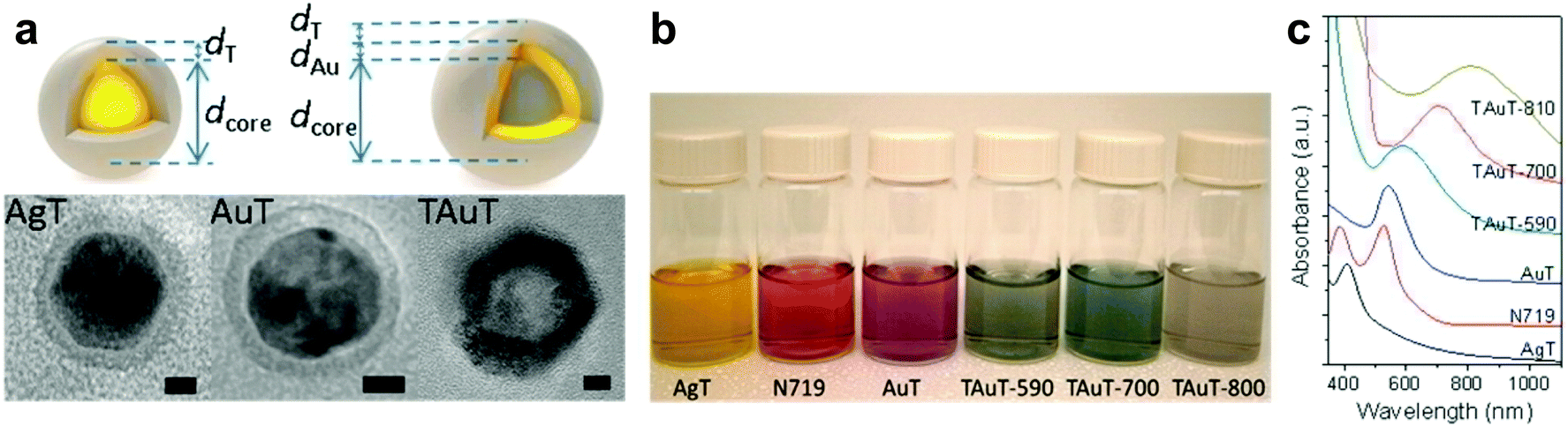
Recently, Jiao and co-workers utilized Au@Ag core@shell bimetallic nanorods (Fig. 11a) in DSSCs and demonstrated that the addition of the Ag layer around the Au nanorod core increased the extinction of the nanostructure.25 The bimetallic nanorods enabled spectral overlap with the 535 nm absorption peak of N719, enhancing light harvesting in the visible, as well as capturing NIR light which the sensitizer does not absorb (Fig. 11b). The bimetallic nanorods increased the PCE by ∼43% with 3.68 wt% of particle density (Fig. 11c). Our group recently demonstrated the use of hybrid bimetallic Au core/Ag shell nanostructures with dual shapes – nanocubes and nanopyramids (Fig. 11d and 1e).30 Dual shapes were dictated by the Au core geometry where the bimetallic nanocubes emerged from rounded-corner nanocube cores and bimetallic nanopyramids emerged from the truncated Au nanocube cores.41 The dual shapes and bimetallic composition gave rise to two distinct dipolar resonances at 530 nm, attributable to the nanocubes, and at 630 nm, attributable to the longitudinal modes of the pyramids (see Fig. 1b). These bimetallic nanostructures directly overlap with the absorption peaks of N719 sensitizer, giving rise to enhanced light scattering and near-field enhancements, and simultaneously absorbing light complementary to the sensitizer absorption, giving rise to broadband light harvesting in the DSSCs. The particle densities of the nanostructures were varied and a systematic increase in light absorption (Fig. 11e) and corresponding trends in photocurrent density (Fig. 11f) were observed. The bimetallic nanostructure resulted in a 27% improvement in DSSC efficiency and was achieved with a nominal 0.44 wt% particle density. This ∼6× decrease in particle density suggests hybrid bimetallic nanostructures have the potential to ultimately achieve high efficiency thin film DSSCs with low materials and processing costs.
 | ||
| Fig. 11 (a) Solar irradiance and extinction of Au nanorods and Au@Ag nanorods. (b) Absorption of TiO2 electrodes with Au@Ag nanoparticles incorporated. (c) Current–potential scans of plasmonic particle incorporated and control DSSCs. Panels a–c adapted with permission from ref. 25. Copyright Royal Society of Chemistry 2015. (d) TEM image of Au@Ag nanostructures designed by our group. (e) Extinction of TiO2 anodes with incorporated Au@Ag nanostructures. (f) Current–potential scans of Au@Ag nanostructure incorporated DSSCs. Panels d–f adapted with permission from ref. 30. Copyright American Chemical Society 2016. | ||
In addition to their role as capping layers, SiO2 and TiO2 have been employed as “nanocarriers” loaded with metal nanoparticles or used to generate multilayered core/shell architectures to achieve broadband absorption. Both SiO2 and TiO2 nanospheres loaded with Au and/or Ag nanoparticles have been reported resulting in >20% improvement in device efficiencies.29,67,155,156 In a unique work by Belcher and co-workers, multilayered TiO2/Au/TiO2 core/shell/shell spherical nanostructures were designed by wet chemical approaches (Fig. 12a). The authors observed that relative to the Au/TiO2 core/shell nanostructures, multilayered geometries enabled highly tunable broadband plasmon resonances resulting in a range of colors and panochromatic photon absorption (Fig. 12b and c).133 By modifying the metal composition (Au or Ag) or altering the thickness of the TiO2 layer plasmonic coupling was extended from near-UV to near-IR. The enhanced tunability of the multilayered “nanoshell” architecture can be understood from the plasmon hybridization model where the core and shell plasmons hybridize to give rise to bonding (bright modes) and antibonding (dark modes). The core to shell ratio determines the energy level splitting between the two modes: a larger splitting results in greater tunability as well as higher sensitivity to the dielectric constant of the surrounding medium. These properties collectively allowed tunability of the multilayered TiO2/Au/TiO2 nanostructures to the near-infrared. The best performing plasmon-enhanced DSSCs resulted in a 10.8% PCE, which is the highest reported to date.
 | ||
| Fig. 12 (a) Schematic and TEM of Ag@TiO2, Au@TiO2 and TiO2@Au@TiO2 core–shell nanoparticles, (scale bar = 5 nm). (b) Optical images demonstrating macroscopic color tunability of core–shell nanoparticles. (c) Extinction spectra of core–shell nanostructures corresponding to different sizes and compositions. Figure adapted with permission from ref. 133. Copyright American Chemical Society 2013. | ||
3.4 Plasmonic nanostructures fabricated by top-down approaches
While the majority of plasmon-enhanced DSSCs reported in the literature have employed wet-chemically synthesized colloidal metal nanoparticles, a number of studies have featured top down fabrication approaches in the design of plasmonic components. Long range nanostructures which support propagating surface plasmon polaritons (SPPs) have been fabricated via nanoimprint lithography,68,157 electron beam lithography (EBL),158,159 and colloidal lithography.160 Analogous to LSPRs, SPPs undergo radiative and non-radiative relaxation mechanisms discussed in Section 2, where the field enhancements can effectively extend up to 1 μm into adjacent dielectric.158,161One of the simplest approaches to implement centimeter-scale plasmonic nanostructures into MSCs is through nanoimprint lithography, in which patterns are imprinted into the mesoporous structure with inverted templates and subsequently filled with metal via evaporation or chemical reduction. McGehee and co-workers used a quartz template to imprint an array of hemispherical wells onto a mesoporous TiO2 substrate and subsequently thermally deposited an Ag cathode that functioned as a nanopatterned plasmonic rear reflector (Fig. 13a).157 The SPP modes generated in these DSSCs enhance light trapping via near field enhancement due to propagating SPPs and scattering from ∼300 nm hemispherical Ag wells. The authors showed calculated enhancement of energy density in the active layer (Fig. 13b) in the lower region (near-field effects) and upper region (scattering), which correlated well with experimental results and overall enhancements observed in the active layer. Further, EBL has also been employed for the fabrication of highly uniform plasmonic nanoarrays to study the interactions between plasmons and TiO2 MSCs. Misawa et al. fabricated a rectangular array of elliptical nanoparticles on a planar TiO2 surface, as shown in Fig. 13c.159 The lack of spectral overlap between the TiO2 substrate and the LSPR implicates that radiative effects and PRET do not play a role in the observed enhancements, indicating that hot carrier transfer allows the plasmonic nanostructures to act as a direct sensitizer to the TiO2. Elliptical nanoparticles support both transverse and longitudinal plasmon modes; each mode can be individually excited with parallel or perpendicular polarized incident light, respectively. The authors activated distinct plasmon modes by polarized light, and subsequent charge generation in TiO2 was observed at either the longitudinal mode or transverse mode as evident in the incident photon to charge carrier efficiency spectra (Fig. 13d). In a similar study, Hägglund et al. enhanced the performance of DSSCs with nanofabricated elliptical gold disks and demonstrated improved efficiency.158
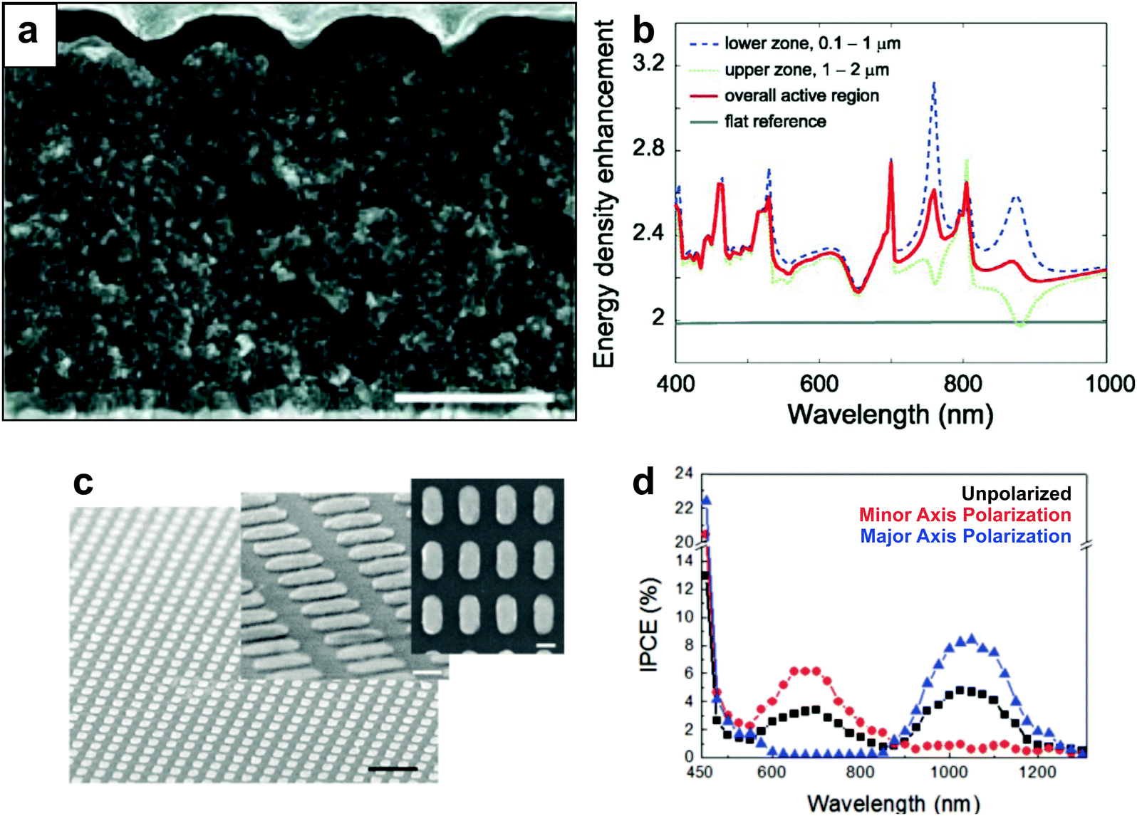 | ||
| Fig. 13 (a) Cross sectional scanning electron micrograph of solid state DSSC with plasmonic nanodome array (scale bar = 1 μm). (b) Calculated energy density enhancement over visible and NIR wavelength ranges. Panels a and b adapted with permission ref. 157. Copyright John Wiley and Sons 2011. (c) Scanning electron micrographs of lithographically fabricated Au nanorods (black scale bar = 500 nm; white scale bar = 100 nm). (d) Incident photon to current efficiency for devices with unpolarized, minor, and major axis polarization. Panels c and d adapted with permission from ref. 159. Copyright American Chemical Society 2010. | ||
Ding et al. used nanoimprint lithography to pattern a square grid into the TiO2 active layer and subsequently filled it with Ag, resulting in a ∼25% enhancement in PCE.68 The authors attribute the enhancement to both plasmonic effects resulting from propagating SPPs facilitated by the periodic Ag array and improved charge transport properties resulting from improved conduction between the TiO2 nanoparticles and increased interfacial area. In another work, Jiang et al. designed a topologically ordered Au counter electrode by first depositing a layer of close packed polystyrene spheres and evaporating Au onto the surface leaving an ordered long range array of Au.160 The authors demonstrated ∼18% increase in PCE, attributed to increased light scattering and subsequent light trapping which was evident from the increased broadband absorption, IPCE, and Jsc.
Top-down approaches are typically not cost-effective for large scale implementation, involve time-consuming processing techniques, and are ineffective in uniformly integrating metal nanostructures throughout the mesoporous active layer. However, top down approaches do provide precise location and orientation of the plasmonic nanostructures and cleaner interfaces with the TiO2 active layer. This enables researchers to perform fundamental studies that will probe the mechanisms of enhancement in MSCs without variations in particle densities or local variations in interparticle distances within the mesoporous layer.
4. Plasmon enhanced perovskite solar cells
Mesoporous perovskite solar cells (PSCs) have diverged rapidly from their predecessors, DSSCs, since 2011. The projected power conversion efficiency (PCE) of PSCs match those of crystalline Si solar cells. A steep increase in PCE has been observed in methylammonium lead halide (MAPbX3, X = Br, Cl, I) perovskites and recently there has been significant interest in using plasmonic enhancement to improve the performance to reach or even surpass the Shockley–Queisser limit. The underlying mechanisms of enhancement are similar to those discussed in Section 2; however, it has been proposed that the presence of LSPRs decreases the exciton binding energy within the perovskite absorber, resulting in higher internal efficiency.162The earliest demonstration of plasmonic enhancement in PSCs was published in 2013 by Snaith and co-workers.162 They mixed SiO2 coated Au nanoparticles into mesoporous Al2O3 scaffold, which improved the photocurrent density by 14.5% with minimal changes in the Voc and FF. The authors correlated the observed enhancement in device performance to a three-fold reduction in exciton binding energy (EB) of the perovskite in the presence of Ag LSPR, as evidenced by photoluminescence. A decrease in EB at the perovskite/metal interface has also been calculated by Wu and co-workers using 3D FDTD simulations, demonstrating that the exciton binding energy in CH3NH3PbI3 is reduced in the presence of copper nanoparticles.163 In another recent study, Snaith and co-workers demonstrated significant spectral enhancement when TiO2 coated Ag nanospheres were embedded in mesoporous Al2O3/perovskite active layer, boosting the measured device efficiencies by ∼20%, with a champion efficiency of 16.3% (Fig. 14a–c).164 Surprisingly, IPCE measurements revealed broadband enhancement over the entire absorption spectrum, rather than in the spectral region of the Ag nanoparticle LSPR (Fig. 14d). The observed enhancement was not correlated to reduction in EB but attributed to the presence of highly polarizable nanoparticles, which improve the radiative decay of excitons and enhance the reabsorption of emitted radiation. This gives rise to increased optical path lengths through light scattering.164 In another study, irregular Au–Ag alloy nanoparticles with a broad resonance peak between 370–800 nm were inserted into a mesoporous TiO2 layer, resulting in a 15.7% increase in PCE.165 Improvements in Voc and FF were attributed to rapid injection of electrons into TiO2, verified by a quenching of photoluminescence lifetimes in the presence of metal NPs.
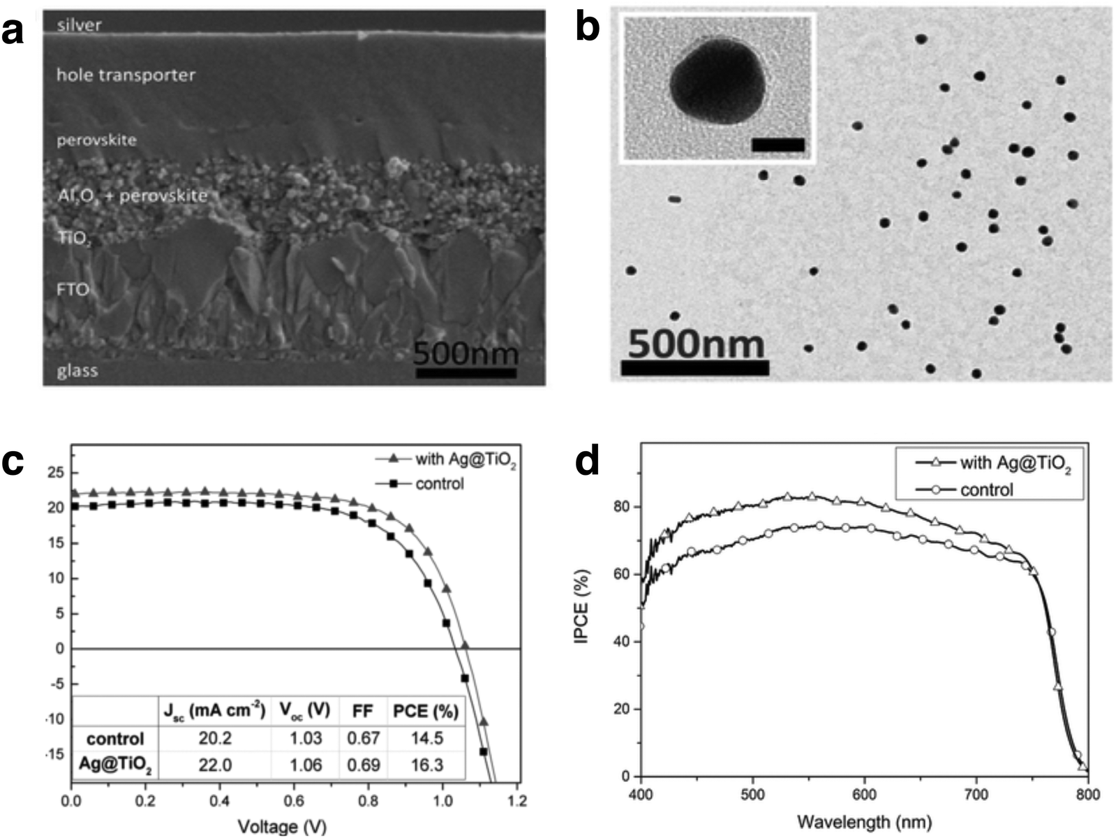 | ||
| Fig. 14 (a) Cross-sectional scanning electron micrograph of a mesoporous perovskite solar cell. (b) TEM image of Ag@TiO2 (inset scale bar = 20 nm). (c) Current–potential scan of control and plasmon-enhanced PSCs. (d) IPCE of control and plasmon enhanced PSCs, indicating broad spectral enhancement with the presence of Ag@TiO2 nanostructures. Figure adapted with permission from ref. 164. Copyright John Wiley and Sons 2015. | ||
Beyond mesoporous architectures, PSCs have also been fabricated in planar geometries, which function much like p–i–n junction solar cells, where the intrinsic layer is the perovskite. Recent efforts in plasmonic enhancement of planar perovskites have shown promising avenues to boost the efficiency and improve charge transport. Sun and co-workers sandwiched Au nanoparticles between two layers of low temperature-processed TiOx film and observed enhanced photocurrent density and external quantum efficiency (EQE).165 The authors attributed the effect to hot electron injection from the plasmonic nanoparticles filling the trap states of TiOx, leading to increased charge carrier density and improved mobility. The group also performed scanning Kelvin probe microscopy, which showed that Au nanoparticles lowered the work function of TiOx and correlated well with the improved Voc in their device performance. Hsu et al. recently compared prismatic silver nanostructures of different sizes and found that the near-infrared resonant (∼700 nm) prisms demonstrated the greatest improvements in PCE, EQE, and Jsc (up to 12% improvement).52 This was likely due to the ability of the nanoprisms to capture light complementary to the MAPbI3−xClx perovskites, resulting in broadband light trapping. Mixed halide, MAPbI3−xClx, perovskite was also used in a recent study where Ag nanoparticles resonant at ∼427 nm were embedded in a PEDOT:PSS hole transport material and interfaced with the perovskite.166 The improved Jsc was attributed to improved hole extraction through the nanoparticles. By a different mechanism, Yan et al. showed that scattering from nanostructured Au electrode improves light capture in the NIR and increases the optical path length of the perovskite active layer.167
Plasmonic enhancement of PSCs has made tremendous strides in only a few years, but many mechanistic questions remain unexplored and would be of significant interest for further study. For example, in a recent work 3D FDTD simulations were performed on nanosphere/perovskite systems, yielding 6–12% absorption enhancement depending on perovskite film thickness.168 This may constitute a theoretical absorption limit, as the study included unusually high particle density (10% as opposed to ∼1% by volume typically used in experiments) and neglects potential negative effects on charge transport by the additional nanoparticles. Furthermore, the spontaneous polarization of perovskite crystals adds both complexity and potential for energy harvesting. This behavior of perovskites not only impacts the type of metal nanostructures used (shape, size, composition control), but also their precise location with respect to the perovskite.169 Baumberg and co-workers recently showed that excitons in 2D organic–inorganic perovskites interact with selective SPP modes of metal nanogratings at specific angles of incident light to produce paired quasiparticles termed “image biexcitons”.170 They showed the exciton mode is spectrally split by Coulomb coupling with its image in the metallic mirror, indicating that controlling the position and polarization of metallic nanosurfaces provides avenues for strong light-matter interactions at the metal/perovskite interface. Beyond coupling metal nanostructures with perovskites, recent evidence also suggests intrinsic plasmonic effects exist within perovskites with quantum confinement in 2D or 3D nanostructures.171 Deeper understanding of the fundamental interactions between plasmonic nanostructures and polarizable perovskites could lead to future optimization of both the light harvesting abilities and charge transport mechanisms in PSCs.166
5. Spectroscopic analyses of fundamental processes
Time-resolved spectroscopic techniques including pump–probe transient absorption spectroscopy (TAS) and time-resolved photoluminescence (TrPL) are powerful approaches to probe and understand fundamental processes occurring in solar cells.172 These spectral techniques enable us to identify and decouple the mechanisms of carrier generation, charge separation, transport, and recombination at various interfaces in MSCs. The use of these techniques is especially critical because, in addition to improving the carrier density, the presence of metal nanostructures also gives rise to other complex phenomena that simultaneously occur in MSCs. In this section, we will summarize the progress made thus far in understanding plasmon-enhanced phenomena in both DSSCs and PSCs with TAS and TrPL. Snaith and co-workers demonstrated one of the first studies on the use of femtosecond spectroscopy to understand the impact of metal nanoparticles in MSCs.22 They performed TAS to probe the effect of 15 nm Au@SiO2 nanoparticles incorporated in DSSCs sensitized with Z907 dye and observed an increase in amplitude of transient absorption in the presence of nanoparticles (Fig. 15a). They attributed this observation to an improvement in photobleaching signal of the dye due to higher molecular absorption coefficient (ε) of Au nanoparticles relative to the sensitizer. The ε of 15 nm Au nanoparticles is ∼109–1010 M−1 cm−1,173 whereas that of Z907 is ∼104 M−1 cm−1. The authors measured the decay kinetics of the photobleaching band at 520 nm and obtained a lifetime of 5 ps, which correlated well with the known electron–phonon relaxation time of ∼3 ps for 15 nm Au nanoparticles. They attributed this fast decay to the relaxation of the hot electron population and further suggested that plasmonic enhancement of photocurrent can only occur if the photoexcited dye transfers carriers into TiO2 in the first tens of femtoseconds before the decoherence of plasmons occurs.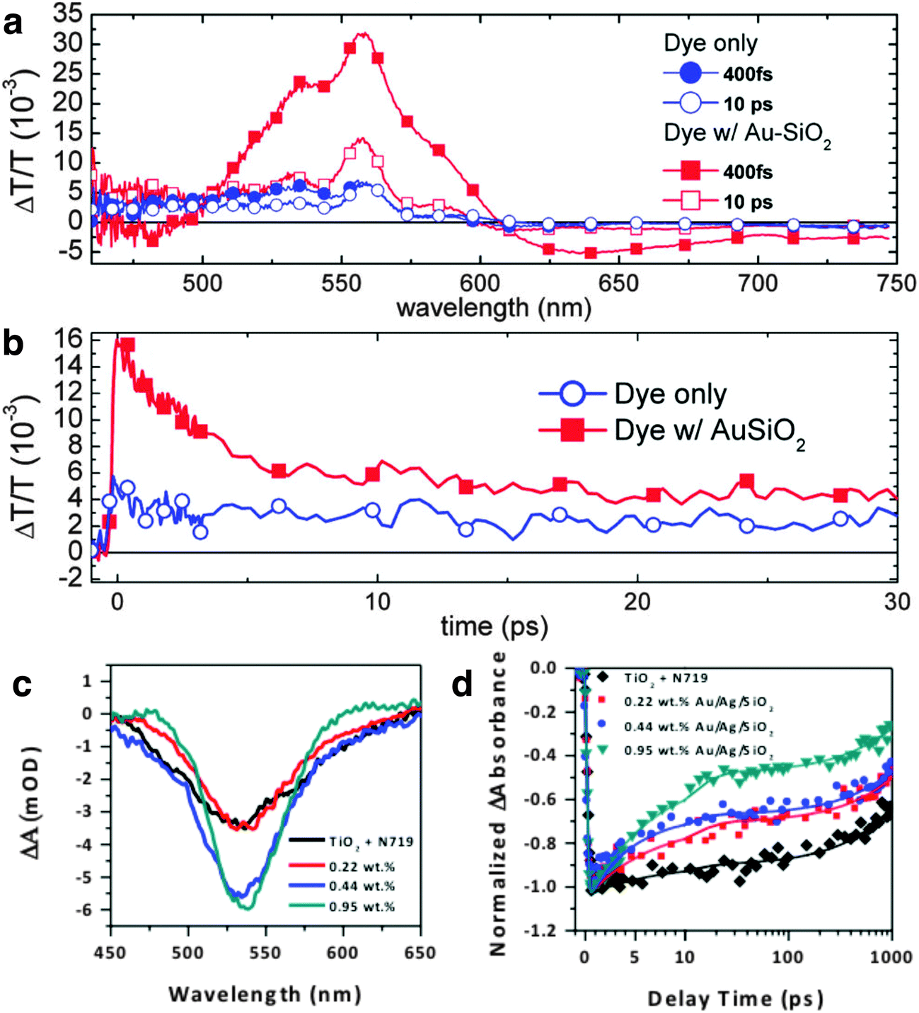 | ||
| Fig. 15 (a) Change in absorption for plasmon-enhanced and control devices 10 ps after excitation. (b) Transient decay profiles of devices at 520 nm with 555 nm excitation. Panels a and b adapted with permission from ref. 22. Copyright American Chemical Society 2011. (c) Transient decay profile pumped at 400 nm and probed at 530 nm of N719 sensitized reference, and plasmon-enhanced DSSC photoanodes with 0.22 wt%, 0.44 wt%, and 0.95 wt% bimetallic Au/Ag nanostructures. The spectra were measured at 1 ps time delay. (d) Decay kinetics at 530 nm for all samples shown in c. All decay kinetics are shown with experimental data (symbols) fitted with a biexponential decay function (smooth line). Panels c and d adapted with permission from ref. 30. Copyright American Chemical Society 2016. | ||
Our group recently demonstrated plasmonic enhancement in DSSCs sensitized with N719 with Au core/Ag shell bimetallic nanostructures, Au@Ag NSs (see Fig. 1e and 11d). We varied the particle density of Au@Ag NSs in DSSCs and examined the dynamics with TAS.30 Due to the strong spectral overlap between Au@Ag NSs (see Fig. 1b) and N719, the observed photobleaching band at 530 nm had contributions from both the photobleaching of the dye and relaxation of the plasmons (Fig. 15c). A correlation between TAS evolutionary spectra and particle density is evident within 1 ps of transient decay. A biexponential fit to the transient decay gave two distinct lifetimes, which we attributed τ1 to electron injection into the conduction band of the TiO2 from the singlet metal to ligand charge transfer (1MLCT) states and τ2 to the triplet (3MLCT) states of the excited N719 complexes.174 An increase in amplitude of the decay kinetics was observed for photoanodes embedded with nanostructures, similar to those observed by Snaith and co-workers; the amplitude monotonically increased with particle density (Fig. 15d). We also correlated this to stronger ε of metal nanostructures relative to N719, which is 1.58 × 10⁴ M−1 cm−1.175 Further, our amplitude-weighted lifetime, τavg, drastically decreased with increasing particle density relative to the reference sample, indicating that Au@Ag NSs improved the light trapping and further enhanced e−/h+ pairs generated in the DSSCs. This gives rise to more carriers being available to transfer to the TiO2 conduction band and faster injection before recombination can occur. The fast carrier injection results in shorter exciton lifetimes.
The mechanisms of plasmonic enhancement have also recently been investigated in PSCs by Zhao and co-workers with steady-state photoluminescence and TrPL.162 The authors compared CH3NH3PbI3−xClx-based PSCs with and without 80 nm Au@SiO2 nanoparticles and observed a significant decrease in steady-state PL (Fig. 16a), and faster decay in TrPL (Fig. 16b) in the presence of the nanoparticles. Further, by comparing PL as a function of temperature for the reference and plasmon-enhanced samples, the authors observed rapid PL quenching with increasing temperature for the samples with Au@SiO2 nanoparticles embedded (Fig. 16c and d). They attributed this phenomenon to a decrease in exciton binding energy (EB) which dropped from 98 meV for the control to 35 meV for the plasmon-enhanced samples. However, more recently the same authors described that for perovskites with already low EB, such as MAPbI3 (10 meV), metal nanoparticles do not appreciably decrease the EB but rather enhance the optical path length by reabsorption of exciton radiation.164 Yuan et al. also observed a significant decrease in steady-state PL and shorter TrPL lifetimes in MAPbI3 based PSCs embedded with Au–Ag alloy popcorn nanoparticles.165 They attributed the observed trends to faster charge transfer at the metal/semiconductor interface, resulting in the suppression of charge recombination.
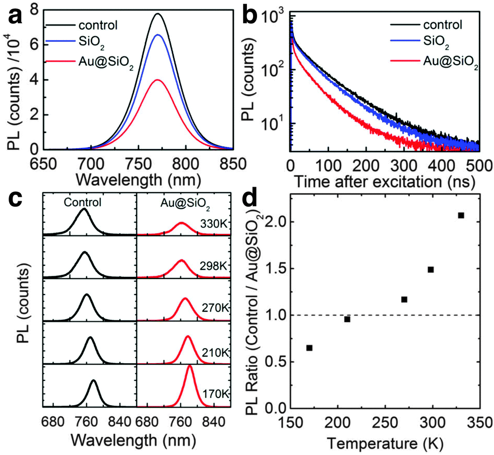 | ||
| Fig. 16 (a) Time-integrated photoluminescence data. (b) Time-resolved photoluminescence decays at 765 nm for perovskite only Al2O3 samples, Au@SiO2 incorporated samples, and SiO2 incorporated samples. (c) Temperature dependent time-integrated photoluminescence of control and Au@SiO2 samples. (d) Ratio of integrated photoluminescence for the control to Au@SiO2 samples. Figure adapted with permission from ref. 162. Copyright American Chemical Society 2013. | ||
Despite the tremendous rise in metal-enhanced MSCs, few studies have used time-resolved spectral techniques to probe fundamental dynamics and understand the foundational principles of plasmonic enhancement. Spectroscopic investigation in both DSSCs and PSCs is necessary comparing the size, shape, and composition effects of plasmonic nanostructures, and the thickness and nature of the surface capping layer (SiO2vs. TiO2 coating) to decouple the mechanisms of PRET, HET, and radiative plasmonic enhancements.
6. Challenges in plasmonic device fabrication
While the past decade has witnessed a promising rise in plasmonic enhancement of solar cells and successful improvements in device efficiencies, several challenges remain both in fabrication of metal nanostructure integrated devices and understanding fundamental phenomena at the metal/sensitizer or metal/semiconductor interface. This section will provide an account of the challenges in this research area and possible ways to surmount these challenges. When metal nanostructures are integrated in DSSCs and PSCs, the optical enhancements must outweigh detrimental electronic and electrochemical effects that arise from (i) recombination of electron–hole pairs on the metal surface, (ii) degradation of the metal during the high temperature annealing of the mesoporous active layer, (iii) corrosion of the metal in contact with the liquid electrolytes used in DSSCs, (iv) reduced absorption in the active layer due to excessive metal particle density, and (v) losses at the metal/sensitizer/TiO2 interface due to inefficient charge injection into the semiconductor, which would decrease device FF and Voc.To mediate these detrimental effects, metal nanostructures are typically coated with a passivation layer of either SiO242,45,110,111 or TiO2.71,131,136,176–183 The electronic effects of the composition and thickness of the passivation layer have been discussed in Section 3.3.3. Thicker dielectric layers (>5 nm) are often preferred as it is easier to synthesize uniform coatings covering the entire metal surface; thicker layers also afford better thermal and chemical stability, and electronic isolation of the nanostructures from the surrounding sensitizer. However, at layer thicknesses >10 nm, plasmon resonance broadening and damping can severely reduce light trapping capabilities. Further, since the electromagnetic fields decay rapidly from the metal surface, the thickness of the capping layer should be controlled to minimize reduction in both radiative enhancement by near-field coupling as well as non-radiative enhancement via PRET. On the contrary, thinner passivation layers of ≤3 nm are strongly desired to not only enable strong coupling with the sensitizer but also allow hot carrier transfer over the oxide tunneling barrier.106 However, achieving controllable, uniform thin oxide layers without aggregating the nanostructures remains a challenge. In addition, hot electron transfer across the Schottky barrier of the semiconductor suffers from internal losses due to heating; the efficiency of this process, however, may be increased by tailoring the semiconductor/metal interface to lower the Schottky barrier. This can be achieved by either introducing another semiconducting layer between the metal nanostructure and TiO2,100 or by introducing molecular bridges184–187 that are known to enhance electrical conductivity and electron transfer, while minimizing electron recombination at trap states localized on the TiO2 surface.188,189
Other challenges in plasmonic enhancement of MSCs include design of metal nanostructures that primarily scatter light with minimal intrinsic absorption losses.190 Since large nanoparticles can be detrimental to charge transport in the solar cell, absorption losses may be minimized by either designing nanostructures with complex morphologies and tunable scattering cross-sections, or by selecting a nanostructure composition with low imaginary component of the dielectric constant. As discussed in Section 3.3, Al is being considered a strong contender to supplement the traditional Au or Ag, although tuning Al resonance beyond the UV remains a challenge. Semiconductor and transparent conducting oxide (TCO) nanostructures that support surface plasmons are also promising candidates for enhancing light trapping in MSCs as discussed in the next section. Finally, optimization of the nanostructure particle densities in MSCs is often challenging but necessary to minimize phonon generation and maintain sufficient absorber volume at high particle densities.30,131
7. The promise of new plasmonic materials beyond noble metals
Beyond the traditional noble metals of Au, Ag, and Cu, recent findings of LSPRs in semiconductor nanocrystals have opened up a new regime in plasmonics, allowing light capture into the far-infrared.191–193 In fact, LSPRs are no longer being viewed solely as attributes of metal nanoparticles, but rather optical characteristics of a collection of free carriers in nanoscale systems. Since the initial discovery by Zhao et al.194 and Luther et al.195 of plasmons in the Cu2−xS nanocrystal family, this burgeoning field has made tremendous strides, and metal-like LSPRs have now been found in oxides, nitrides, tellurides, sulfides, and selenides.196–208 LSPRs in semiconductors are generated in three possible ways: (i) by introducing free carriers extrinsically in the form of dopant atoms, such as those in oxides and nitrides (Al:ZnO, ITO, etc.);201–204,206,207 (ii) by “self-doping” intrinsically where free carriers arise from variable oxidation state of the element in non-stoichiometric phase, such as in copper chalcogenides (Cu2−xS, Cu2−xSe, Cu2−xTe etc.)194–198,200,208 and oxygen-deficient metal oxides (WO3−x, MoO3−x);199,201,205 and (iii) by strongly correlated electrons where free carriers arise due to the intrinsic electronic structure of the semiconductor, giving rise to conductive behavior, such as in transition metal dioxides (VO2, RuO2).Plasmons in semiconductor nanocrystals have several unique features. First, noble metals have high carrier densities (1023 cm−3) that cannot be appreciably altered; however, carrier concentrations in semiconductors can be varied from 1016 to 1021 cm−3 by controlled doping enabling very high tunability of LSPRs from the near-infrared to THz regime. And second, noble metals have high optical losses due to both interband and intraband transitions. On the contrary, semiconductors qualify as low-loss materials due to their large bandgap, which ensures almost no interband transition losses, and lower imaginary part of the permittivity in the infrared which significantly reduces intraband losses.191,193,209 These qualifications collectively suggest LSPRs in semiconductor nanocrystals can be manipulated to generate desirable optical properties to enhance light harvesting in MSCs. A recent work by Rosenthal and co-workers demonstrated this effect; the authors compared the performance of degenerately doped plasmonic CuxInyS2 quantum dots with its non-plasmonic counterpart (no cationic vacancies) in solar cells and observed an 11.5% relative increase in IPCE with the former.200 However, despite their promise, the full potential of semiconductor LSPRs in solar cells has yet to be realized due to their poor tunability in the visible region and lower carrier densities than traditional metal nanoparticles, resulting in minimal light scattering. These challenges have been addressed with recent efforts in metal–semiconductor hybrids either in core/shell architectures or dimer geometries.210–213 The unique combination of metal and semiconductor components on a single nanoplatform enables broadband tunability of optical resonances from UV to IR, and provides three degrees of freedom for manipulating LSPRs – shape, size, and modification of carrier density by controlling vacancies. However, these nanostructures have not been employed in solar cells yet to evaluate their device performance and IPCE behavior. While detailed discussion of semiconductor plasmonics and their relevance in MSCs is beyond the scope of this review, readers are encouraged to refer to thorough reviews already published on this topic.191,192,209,214,215
8. Other plasmonic photovoltaic systems
While this review article primarily focuses on mesoporous dye-sensitized and perovskite solar cells, plasmonic nanostructures have improved light harvesting in other solar energy conversion systems including photoelectrochemical water splitting,46 and thin film photovoltaic architectures such as silicon solar cells and organic photovoltaics.216 Whereas the plasmonic enhancement mechanisms in water splitting are essentially the same as liquid-electrolyte based mesoporous solar cells, in planar photovoltaic architectures plasmonic enhancements are correlated to the minority carrier diffusion lengths. Similar to MSCs, both light scattering and near-field generation play a crucial role in thin film solar cells. However, the minority carrier diffusion lengths of the plasmonically enhanced excitons must be larger than the thickness of the active layer for the carriers to be collected. Hot electron transfer may also be envisioned in planar PVs specifically if metal nanostructures are placed at the interface of the active layer and charge transport layer. Unlike mesoporous solar cells where plasmonic enhancement is largely achieved by incorporating discrete nanostructures supporting LSPRs, the planar architecture of thin-film PVs allows integration of waveguide structures that support SPP modes resulting in improved optical path length of the devices. The planar geometry is also ideal to integrate plasmonic antireflection coatings to enable coupling of back-scattered light. Unlike traditional dielectric coatings, plasmonic antireflection coatings are highly tunable via geometry, composition, and surrounding dielectric medium. Further, these coatings can be designed to improve the angular response of a planar solar cell. An important aspect of incorporating plasmonic components in all classes of solar cells is the enhanced light harvesting enables the design of thinner active layers without sacrificing absorption; this effect is even more prominent in thin film PVs. Therefore plasmon-enhanced PVs are ultimately expected to yield more economical solar cells with smaller footprint. Since this review specifically focuses on mesoporous solar cells, an in depth review of plasmon-enhanced thin film PVs is beyond the scope of this article. However, readers are directed to other excellent reviews that cover these topics.217–2239. Summary and future prospects
This review article provides a comprehensive overview of progress in plasmon-enhanced mesoporous solar cells (MSCs), including perovskite solar cells (PSCs) and dye-sensitized solar cells (DSSCs), in the past decade. We have discussed the mechanisms of radiative and non-radiative plasmonic-enhancement, including light scattering and near-field coupling, as well as hot electron transfer (HET) and plasmon resonant energy transfer (PRET) and their relevance in MSCs. A survey of the literature demonstrates DSSCs primarily benefit from radiative enhancement both in the near-field and far-field, as well as PRET resulting in increased photocurrent. In PSCs, plasmon-enhanced light harvesting gives rise to a modest increase in photocurrent, by both enhancing optical absorption and decreasing exciton binding energy. Recent evidence also shows HET from plasmons to perovskites drives an increase in open circuit voltage, improving overall device performance, but further work is required to confirm this hypothesis. We also discuss the challenges in integration of plasmonic nanostructures in MSCs and surface passivation techniques to surmount these challenges. Further, we provide a brief overview of LSPRs in semiconductor nanocrystals and their promise in MSCs as low-loss, highly-tunable optical materials. Finally, distinct from other reviews, we also summarize the progress in spectroscopic investigation of plasmon-enhanced DSSCs and PSCs with time-resolved spectroscopies to probe fundamental charge transport and other optically-induced phenomena.Plasmonic enhancement in solar cells has progressed rapidly in the past decade from thin-film Si photovoltaics (PVs) to perovskite devices. We anticipate in the next decade, new plasmonic materials will be discovered, and new PV architectures will be realized for further advances in efficiency and ultimately in commercial feasibility. Specifically, integrating mixed-halide organic–inorganic and all-inorganic perovskites with plasmonic nanostructures is very promising. The high air- and moisture-stability of MAPbI3−xBrx perovskite relative to their pure iodide counterpart is highly desirable for commercialization; however, mixed-halides typically have their band-edge in the visible.10,224–227 By coupling plasmonic nanostructures resonant in the IR with MAPbI3−xBrx, broadband solar light capture can be realized. Further, plasmonic enhancement via HET will likely be possible since a direct overlap of LSPR and perovskite absorption is not required. LSPRs may also be engineered into the cathode of PSCs, which is typically Au or Ag, by nanostructuring the electrode with top-down approaches to ultimately enable long-range SPP modes to couple to the optical resonances of the perovskites. Finally, further understanding of charge transport processes at the dye/metal and perovskite/metal interfaces with time-resolved spectroscopies is necessary to probe electronic processes at early time-scales. Single-particle measurements at these interfaces with super-resolution imaging would also be highly relevant to minimize ambiguities in ensemble measurements.
Acknowledgements
WRE acknowledges support from the National Science Foundation Graduate Research Fellowship Program under Grant Number 1445197. HFZ acknowledges support from NSF EPSCOR (NSF EPS1004083), NSF BRIGE (EEC 1342185), and the Department of Education for a Graduate Assistance in Areas of National Need (GAANN) Fellowship under grant number P0200A090323.References
- B. E. Hardin, H. J. Snaith and M. D. McGehee, Nat. Photonics, 2012, 6, 162–169 CrossRef CAS.
- M. Grätzel, Acc. Chem. Res., 2009, 42, 1788–1798 CrossRef PubMed.
- S. Kazim, M. K. Nazeeruddin, M. Gratzel and S. Ahmad, Angew. Chem., Int. Ed., 2014, 53, 2812–2824 CrossRef CAS PubMed.
- J. Burschka, N. Pellet, S.-J. Moon, R. Humphry-Baker, P. Gao, M. K. Nazeeruddin and M. Gratzel, Nature, 2013, 499, 316–332 CrossRef CAS PubMed.
- I. Chung, B. Lee, J. He, R. P. H. Chang and M. G. Kanatzidis, Nature, 2012, 485, 486–489 CrossRef CAS PubMed.
- M. Law, L. E. Greene, J. C. Johnson, R. Saykally and P. Yang, Nat. Mater., 2005, 4, 455–459 CrossRef CAS PubMed.
- S. Mathew, A. Yella, P. Gao, R. Humphry-Baker, B. F. E. Curchod, N. Ashari-Astani, I. Tavernelli, U. Rothlisberger, M. K. Nazeeruddin and M. Grätzel, Nat. Chem., 2014, 6, 242–247 CrossRef CAS PubMed.
- A. Yella, H. W. Lee, H. N. Tsao, C. Yi, A. K. Chandiran, M. K. Nazeeruddin, E. W. D. Diau, C. Y. Yeh, S. M. Zakeeruddin and M. Grätzel, Science, 2011, 334, 629–634 CrossRef CAS PubMed.
- J.-H. Yum, E. Baranoff, S. Wenger, M. K. Nazeeruddin and M. Grätzel, Energy Environ. Sci., 2011, 4, 842–857 CAS.
- M. M. Lee, J. Teuscher, T. Miyasaka, T. N. Murakami and H. J. Snaith, Science, 2012, 338, 643–648 CrossRef CAS PubMed.
- J. M. Ball, M. M. Lee, A. Hey and H. J. Snaith, Energy Environ. Sci., 2013, 6, 1739–1743 CAS.
- W. A. Laban and L. Etgar, Energy Environ. Sci., 2013, 6, 3249–3253 CAS.
- P. Qin, S. Tanaka, S. Ito, N. Tetreault, K. Manabe, H. Nishino, M. K. Nazeeruddin and M. Gratzel, Nat. Commun., 2014, 5, 3834 CAS.
- J. H. Heo, S. H. Im, J. H. Noh, T. N. Mandal, C.-S. Lim, J. A. Chang, Y. H. Lee, H.-j. Kim, A. Sarkar, M. K. Nazeeruddin, M. Grätzel and S. I. Seok, Nat. Photonics, 2013, 7, 486–491 CrossRef CAS.
- M. Liu, M. B. Johnston and H. J. Snaith, Nature, 2013, 501, 395–399 CrossRef CAS PubMed.
- H. J. Snaith, J. Phys. Chem. Lett., 2013, 4, 3623–3630 CrossRef CAS.
- J. B. Baxter, J. Vac. Sci. Technol., A, 2012, 30, 020801 Search PubMed.
- M. A. Green and S. Pillai, Nat. Photonics, 2012, 6, 130–132 CrossRef CAS.
- A. Polman and H. A. Atwater, Nat. Mater., 2012, 11, 174–177 CrossRef CAS PubMed.
- H. A. Atwater and A. Polman, Nat. Mater., 2010, 9, 205–213 CrossRef CAS PubMed.
- G. W. P. Adhyaksa, S.-W. Baek, G. I. Lee, D. K. Lee, J.-Y. Lee and J. K. Kang, ChemSusChem, 2014, 7, 2461–2468 CrossRef CAS PubMed.
- M. D. Brown, T. Suteewong, R. S. S. Kumar, V. D. Innocenzo, A. Petrozza, M. M. Lee, U. Wiesner and H. J. Snaith, Nano Lett., 2011, 11, 438–445 CrossRef CAS PubMed.
- P.-Y. Chen, X. Dang, M. T. Klug, J. Qi, D. Courchesne, F. J. Burpo, N. Fang, P. T. Hammond and A. M. Belcher, ACS Nano, 2013, 6563–6574 CrossRef CAS PubMed.
- B. Ding, B. J. Lee, M. Yang, H. S. Jung and J. K. Lee, Adv. Energy Mater., 2011, 1, 415–421 CrossRef CAS.
- H. Dong, Z. Wu, A. El-Shafei, B. Xia, J. Xi, S. Ning, B. Jiao and X. Hou, J. Mater. Chem. A, 2015, 3, 4659–4668 CAS.
- J. Du, J. Qi, D. Wang and Z. Tang, Energy Environ. Sci., 2012, 5, 6914–6918 CAS.
- Y. H. Jang, Y. J. Jang, S. T. Kochuveedu, M. Byun, Z. Lin and D. H. Kim, Nanoscale, 2014, 6, 1823–1832 RSC.
- S. Wooh, Y.-G. Lee, M. N. Tahir, D. Song, M. Meister, F. Laquai, W. Tremel, J. Bisquert, Y. S. Kang and K. Char, J. Mater. Chem. A, 2013, 1, 12627–12634 CAS.
- J. Yun, S. H. Hwang and J. Jang, ACS Appl. Mater. Interfaces, 2015, 7, 2055–2063 CAS.
- H. F. Zarick, W. R. Erwin, A. Boulesbaa, O. Hurd, J. A. Webb, A. Puretzky, D. Geohegan and R. Bardhan, ACS Photonics, 2016 DOI:10.1021/acsphotonics.5b00552.
- C. F. Bohren and D. R. Huffman, Absorption and Scattering of Light by Small Particles, Wiley, 1983 Search PubMed.
- S. A. Maier, Plasmonics: Fundamentals and Applications, Springer, 2007 Search PubMed.
- H. C. van de Hulst, Light Scattering by Small Particles, Dover Publications, Inc., New York, N.Y., 1981 Search PubMed.
- L. Novotny and N. v. Hulst, Nat. Photonics, 2011, 5, 83–90 CrossRef CAS.
- K. L. Kelly, E. Coronado, L. L. Zhao and G. C. Schatz, J. Phys. Chem. B, 2003, 107, 668–677 CrossRef CAS.
- V. Myroshnychenko, J. Rodrıguez-Fernandez, I. Pastoriza-Santos, A. M. Funston, C. Novo, P. Mulvaney, L. M. Liz-Marzan and F. J. G. d. Abajo, Chem. Soc. Rev., 2008, 37, 1792–1805 RSC.
- P. K. Jain, K. S. Lee, I. H. El-Sayed and M. A. El-Sayed, J. Phys. Chem. B, 2006, 110, 7238–7248 CrossRef CAS PubMed.
- J. M. Pitarke, V. M. Silkin, E. V. Chulkov and P. M. Echenique, J. Opt. A: Pure Appl. Opt., 2005, 7, S73–S84 CrossRef CAS.
- M. Rycenga, C. M. Cobley, J. Zeng, W. Li, C. H. Moran, Q. Zhang, D. Qin and Y. Xia, Chem. Rev., 2011, 111, 3669–3712 CrossRef CAS PubMed.
- S. Linic, P. Christopher and D. B. Ingram, Nat. Mater., 2011, 10, 911–921 CrossRef CAS PubMed.
- H. F. Zarick, W. R. Erwin, J. Aufrecht, A. Coppola, B. R. Rogers, C. L. Pint and R. Bardhan, J. Mater. Chem. A, 2014, 2, 7088–7098 CAS.
- J. A. Webb, W. R. Erwin, H. F. Zarick, J. Aufrecht, H. W. Manning, M. J. Lang, C. L. Pint and R. Bardhan, J. Phys. Chem. C, 2014, 118, 3696–3707 CAS.
- R. Carminati, J. J. Greffet, C. Henkel and J. M. Vigoureux, Opt. Commun., 2006, 261, 368–375 CrossRef CAS.
- P. K. Jain, W. Huang and M. A. El-Sayed, Nano Lett., 2007, 7, 2080–2088 CrossRef CAS.
- J. R. Lakowicz, Anal. Biochem., 2005, 337, 171–194 CrossRef CAS PubMed.
- S. C. Warren and E. Thimsen, Energy Environ. Sci., 2012, 5, 5133 CAS.
- A. V. Zayats, I. I. Smolyaninov and A. A. Maradudin, Phys. Rep., 2005, 408, 131–314 CrossRef CAS.
- W.-S. Chang, B. a. Willingham, L. S. Slaughter, B. P. Khanal, L. Vigderman, E. R. Zubarev and S. Link, Proc. Natl. Acad. Sci. U. S. A., 2011, 108, 19879–19884 CrossRef CAS PubMed.
- J. A. Fan, C. Wu, K. Bao, J. Bao, R. Bardhan, N. J. Halas, V. N. Manoharan, P. Nordlander, G. Shvets and F. Capasso, Science, 2010, 328, 1135–1138 CrossRef CAS PubMed.
- A. Tao, P. Sinsermsuksakul and P. Yang, Nat. Nanotechnol., 2007, 2, 435–440 CrossRef CAS PubMed.
- M. K. Gangishetty, R. W. J. Scott and T. L. Kelly, Langmuir, 2014, 30, 14352–14359 CrossRef CAS PubMed.
- H.-L. Hsu, T.-Y. Juang, C.-P. Chen, C.-M. Hsieh, C.-C. Yang, C.-L. Huang and R.-J. Jeng, Sol. Energy Mater. Sol. Cells, 2015, 140, 224–231 CrossRef CAS.
- The Mie Theory: Basics and Applications, ed. W. Hergert and T. Wriedt, Springer, New York, NY, 2012 Search PubMed.
- W. T. Doyle, Phys. Rev. B: Condens. Matter Mater. Phys., 1989, 39, 9852–9858 CrossRef.
- X. Fan, W. Zheng and D. J. Singh, Light: Sci. Appl., 2014, 3, e179 CrossRef CAS.
- Q. Fu and W. Sun, Appl. Opt., 2001, 40, 1354–1361 CrossRef CAS PubMed.
- C. Sönnichsen, T. Franzl, T. Wilk, G. v. Plessen and J. Feldmann, New J. Phys., 2002, 4, 93 CrossRef.
- K.-S. Lee and M. A. El-Sayed, J. Phys. Chem. B, 2006, 110, 19220–19225 CrossRef CAS PubMed.
- E. Hao, G. C. Schatz and J. T. Hupp, J. Fluoresc., 2004, 14, 331–341 CrossRef CAS PubMed.
- I. O. Sosa, C. Noguez and R. G. Barrera, J. Phys. Chem. B, 2003, 107, 6269–6275 CrossRef CAS.
- R. Bardhan, S. Mukherjee, N. Mirin, S. D. Levit, P. Nordlander and N. J. Halas, J. Phys. Chem. C, 2010, 114, 7378–7383 CAS.
- N. K. Grady, N. J. Halas and P. Nordlander, Chem. Phys. Lett., 2004, 399, 167–171 CrossRef CAS.
- P. B. Johnson and R. W. Christy, Phys. Rev. B: Solid State, 1972, 6, 4370–4379 CrossRef CAS.
- A. Pinchuk, G. V. Plessen and U. Kreibig, J. Phys. D: Appl. Phys., 2004, 37, 3133–3139 CrossRef CAS.
- J. M. Pitarke, V. M. Silkin, E. V. Chulkov and P. M. Echenique, Rep. Prog. Phys., 2007, 70, 1–87 CrossRef CAS.
- H. Dong, Z. Wu, F. Lu, Y. Gao, A. El-Shafei, B. Jiao, S. Ning and X. Hou, Nano Energy, 2014, 10, 181–191 CrossRef CAS.
- S. H. Hwang, D. H. Shin, J. Yun, C. Kim, M. Choi and J. Jang, Chemistry, 2014, 20, 4439–4446 CrossRef CAS PubMed.
- W. Jiang, H. Liu, L. Yin and Y. Ding, J. Mater. Chem. A, 2013, 1, 6433–6440 CAS.
- H. Y. Kim, W. Y. Rho, H. Y. Lee, Y. S. Park and J. S. Suh, Sol. Energy, 2014, 109, 61–69 CrossRef CAS.
- B. Lim, H. Yun, S. Kwon, Y. Kim and D. S. Chung, RSC Adv., 2014, 4, 48236–48244 RSC.
- S. J. Lin, K. C. Lee, J. L. Wu and J. Y. Wu, Appl. Phys. Lett., 2011, 99, 043306 CrossRef.
- S. J. Lin, K. C. Lee, J. L. Wu and J. Y. Wu, Sol. Energy, 2012, 86, 2600–2605 CrossRef CAS.
- K.-S. Lee and M. A. El-Sayed, J. Phys. Chem. B, 2005, 109, 20331–20338 CrossRef CAS PubMed.
- A. Liebsch and B. N. J. Persson, J. Phys. C: Solid State Phys., 1983, 16, 5375–5391 CrossRef CAS.
- S. Link, M. B. Mohamed and M. A. El-Sayed, J. Phys. Chem. B, 1999, 103, 3073–3077 CrossRef CAS.
- F. Wang and Y. R. Shen, Phys. Rev. Lett., 2006, 97, 206806 CrossRef PubMed.
- T. R. Jensen, M. L. Duval, K. L. Kelly, A. A. Lazarides, G. C. Schatz and R. P. Van Duyne, J. Phys. Chem. B, 1999, 103, 9846–9853 CrossRef CAS.
- H. F. Zarick, O. Hurd, J. A. Webb, C. Hungerford, W. R. Erwin and R. Bardhan, ACS Photonics, 2014, 1, 806–811 CrossRef CAS.
- J. A. Schuller, E. S. Barnard, W. Cai, Y. C. Jun, J. S. White and M. l. Brongersma, Nat. Mater., 2010, 9, 193–204 CrossRef CAS PubMed.
- M. Haggui, M. Dridi, J. Plain, S. Marguet, H. Perez, G. C. Schatz, G. P. Wiederrecht, S. K. Gray and R. Bachelot, ACS Nano, 2012, 6, 1299–1307 CrossRef CAS PubMed.
- M. Rycenga, X. Xia, C. H. Moran, F. Zhou, D. Qin, Z. Y. Li and Y. Xia, Angew. Chem., Int. Ed., 2011, 50, 5473–5477 CrossRef CAS PubMed.
- M. Rycenga, M. H. Kim, P. H. Camargo, C. Cobley, Z. Y. Li and Y. Xia, J. Phys. Chem. A, 2009, 113, 3932–3939 CrossRef CAS PubMed.
- M. B. Mohamed, V. Volkov, S. Link and M. a. El-Sayed, Chem. Phys. Lett., 2000, 317, 517–523 CrossRef CAS.
- J. Gersten and A. Nitzan, J. Chem. Phys., 1980, 73, 3023–3037 CrossRef CAS.
- P. F. Liao and A. Wokaun, J. Chem. Phys., 1982, 76, 751–752 CrossRef CAS.
- M. W. Knight, H. Sobhani, P. Nordlander and N. J. Halas, Science, 2011, 332, 702–704 CrossRef CAS PubMed.
- J. Li, S. K. Cushing, F. Meng, T. R. Senty, A. D. Bristow and N. Wu, Nat. Photonics, 2015, 9, 601–607 CrossRef CAS.
- C. Clavero, Nat. Photonics, 2014, 8, 95–103 CrossRef CAS.
- X. Li, D. Xiao and Z. Zhang, New J. Phys., 2013, 15, 023011 CrossRef.
- R. Bingham, J. Mendonça and J. Dawson, Phys. Rev. Lett., 1997, 78, 247–249 CrossRef CAS.
- Y. Gao, Z. Yuan and S. Gao, J. Chem. Phys., 2011, 134, 1–5 Search PubMed.
- M. L. Brongersma, N. J. Halas and P. Nordlander, Nat. Nanotechnol., 2015, 10, 25–34 CrossRef CAS PubMed.
- A. Manjavacas, J. G. Liu, V. Kulkarni and P. Nordlander, ACS Nano, 2014, 7630–7638 CrossRef CAS PubMed.
- R. Bardhan, W. Chen, M. Bartels, C. Perez-Torres, M. F. Botero, R. W. McAninch, A. Contreras, R. Schiff, R. G. Pautler, N. J. Halas and A. Joshi, Nano Lett., 2010, 10, 4920–4928 CrossRef CAS PubMed.
- R. Bardhan, W. Chen, C. Perez-Torres, M. Bartels, R. M. Huschka, L. Zhao, E. Morosan, R. Pautler, A. Joshi and N. J. Halas, Adv. Funct. Mater., 2009, 19, 3901–3909 CrossRef CAS.
- R. Bardhan, S. Lal, A. Joshi and N. J. Halas, Acc. Chem. Res., 2011, 44, 936–946 CrossRef CAS PubMed.
- W. Chen, C. Ayala-Orozco, N. C. Biswal, C. Perez-Torres, M. Bartels, R. Bardhan, G. Stinnet, X.-D. Liu, B. Ji, A. Deorukhkar, L. V. Brown, S. Guha, R. G. Pautler, S. Krishnan, N. J. Halas and A. Joshi, Nanomedicine, 2014, 9, 1209–1222 CrossRef CAS PubMed.
- M.-R. Choi, R. Bardhan, K. J. Stanton-Maxey, H. N. S. Badve, K. M. Stantz, N. Cao, N. J. Halas and S. E. Clare, Cancer Nanotechnol., 2012, 3, 47–54 CrossRef CAS PubMed.
- J. A. Webb and R. Bardhan, Nanoscale, 2014, 6, 2502–2530 RSC.
- K. Wu, J. Chen, J. R. McBride and T. Lian, Science, 2015, 349, 3584–3588 CrossRef PubMed.
- M. W. Knight, Y. Wang, A. S. Urban, A. Sobhani, B. Y. Zheng, P. Nordlander and N. J. Halas, Nano Lett., 2013, 13, 1687–1692 CrossRef CAS PubMed.
- S. Mubeen, J. Lee, W.-R. Lee, N. Singh, G. D. Stucky and M. Moskovits, ACS Nano, 2014, 8, 6066–6073 CrossRef CAS PubMed.
- S. Mubeen, J. Lee, N. Singh, S. Krämer, G. D. Stucky and M. Moskovits, Nat. Nanotechnol., 2013, 8, 247–251 CrossRef CAS PubMed.
- S. Mukherjee, L. Zhou, A. M. Goodman, N. Large, C. Ayala-Orozco, Y. Zhang, P. Nordlander and N. J. Halas, J. Am. Chem. Soc., 2014, 136, 64–67 CrossRef CAS PubMed.
- A. Sobhani, M. W. Knight, Y. Wang, B. Zheng, N. S. King, L. V. Brown, Z. Fang, P. Nordlander and N. J. Halas, Nat. Commun., 2013, 4, 1643 CrossRef PubMed.
- W. R. Erwin, A. Coppola, H. F. Zarick, P. Arora, K. J. Miller and R. Bardhan, Nanoscale, 2014, 6, 12626–12634 RSC.
- A. O. Govorov, H. Zhang and Y. K. Gun'Ko, J. Phys. Chem. C, 2013, 117, 16616–16631 CAS.
- S. Mukherjee, H. Sobhani, J. B. Lassitter, R. Bardhan, P. Nordlander and N. J. Halas, Nano Lett., 2010, 10, 2694–2701 CrossRef CAS PubMed.
- Z. Fang, J. Cai, Z. Yan, P. Nordlander, N. J. Halas and X. Zhu, Nano Lett., 2011, 11, 4475–4479 CrossRef CAS PubMed.
- F. Hao, P. Nordlander, Y. Sonnefraud, P. Van Dorpe and S. a. Maier, ACS Nano, 2009, 3, 643–652 CrossRef CAS PubMed.
- F. Hao, Y. Sonnefraud, P. Van Dorpe, S. A. Maier, N. J. Halas and P. Nordlander, Nano Lett., 2008, 8, 3983–3988 CrossRef CAS PubMed.
- J. A. Fan, K. Bao, C. Wu, J. Bao, R. Bardhan, N. J. Halas, V. N. Manoharan, G. Shvets, P. Nordlander and F. Capasso, Nano Lett., 2010, 10, 4680–4685 CrossRef CAS PubMed.
- J. B. Lassiter, H. Sobhani, J. A. Fan, J. Kundu, F. Capasso, P. Nordlander and N. J. Halas, Nano Lett., 2010, 10, 3184–3189 CrossRef CAS PubMed.
- M. Hentschel, D. Dregely, R. Vogelgesang, H. Giessen and N. Liu, ACS Nano, 2011, 5, 2042–2050 CrossRef CAS PubMed.
- S. K. Cushing, J. Li, J. Bright, B. T. Yost, P. Zheng, A. D. Bristow and N. Wu, J. Phys. Chem. C, 2015, 119, 16239–16244 CAS.
- S. K. Cushing, J. Li, F. Meng, T. R. Senty, S. Suri, M. Zhi, M. Li, A. D. Bristow and N. Wu, J. Am. Chem. Soc., 2012, 134, 15033–15041 CrossRef CAS PubMed.
- A. Pinchuk and U. Kreibig, New J. Phys., 2003, 5, 151.151 CrossRef.
- H. Choi, W. T. Chen and P. Kamat, ACS Nano, 2012, 6, 4418–4427 CrossRef CAS PubMed.
- Q. Wang, T. Butburee, X. Wu, H. J. Chen, G. Liu and L. Z. Wang, J. Mater. Chem. A, 2013, 1, 13524–13531 CAS.
- A. Anderson, K. S. Deryckx, X. G. Xu, G. Steinmeyer and M. B. Raschke, Nano Lett., 2010, 10, 2519–2524 CrossRef CAS PubMed.
- Y. Nishiyama, K. Imaeda, K. Imura and H. Okamoto, J. Phys. Chem. C, 2015, 119, 16125–16222 Search PubMed.
- C. Sönnichsen, T. Franzl, T. Wilk, G. von Plessen, J. Feldmann, O. Wilson and P. Mulvaney, Phys. Rev. Lett., 2002, 88, 077402 CrossRef PubMed.
- C. Wen, K. Ishikawa, M. Kishima and K. Yamada, Sol. Energy Mater. Sol. Cells, 2000, 61, 339–351 CrossRef CAS.
- C. Noguez, J. Phys. Chem. C, 2007, 111, 3806–3819 CAS.
- C. H. Lin and C. W. Liu, Sensors, 2013, 10, 8797–8826 CrossRef PubMed.
- Y. H. Su, Y. F. Ke, S. L. Cai and Q. Y. Yao, Light: Sci. Appl., 2012, 1, e14(15) CrossRef.
- D. Zheng, X. Pang, M. Wang, Y. He, C. Lin and Z. Lin, Chem. Mater., 2015, 27, 5271–5278 CrossRef CAS.
- A. Dabirian and N. Taghavinia, ACS Appl. Mater. Interfaces, 2015, 7, 14926–14932 CAS.
- C. Nahm, H. Choi, J. Kim, D. R. Jung, C. Kim, J. Moon, B. Lee and B. Park, Appl. Phys. Lett., 2011, 99, 253107 CrossRef.
- Q. Xu, F. Liu, Y. Liu, K. Cui, X. Feng, W. Zhang and Y. Huang, Sci. Rep., 2013, 3, 2112 Search PubMed.
- N. Chander, A. F. Khan, E. Thouti and S. K. Sardana, Sol. Energy, 2014, 109, 11–23 CrossRef CAS.
- S. Chang, Q. Li, X. Xiao, K. Y. Wong and T. Chen, Energy Environ. Sci., 2012, 5, 9444–9448 CAS.
- X. Dang, J. Qi, M. T. Klug, P.-Y. Chen, D. S. Yun, N. X. Fang, P. T. Hammond and A. M. Belcher, Nano Lett., 2013, 13, 637–642 CrossRef CAS PubMed.
- S. W. Sheehan, H. Noh, G. W. Brudvig, H. Cao and C. A. Schmuttenmaer, J. Phys. Chem. C, 2013, 117, 927–934 CAS.
- M. K. Gangishetty, K. E. Lee, R. W. J. Scott and T. L. Kelly, ACS Appl. Mater. Interfaces, 2013, 5, 11044–11051 CAS.
- W.-L. Liu, F.-C. Lin, Y.-C. Yang, C.-H. Huang, S. Gwo, M. H. Huang and J.-S. Huang, Nanoscale, 2013, 5, 7953–7962 RSC.
- K. A. Willets and R. P. Van Duyne, Annu. Rev. Phys. Chem., 2007, 58, 267–297 CrossRef CAS PubMed.
- B. Lim and Y. Xia, Angew. Chem., Int. Ed., 2011, 50, 76–85 CrossRef CAS PubMed.
- C. Burda, X. Chen, R. Narayanan and M. A. El-Sayed, Chem. Rev., 2005, 105, 1025–1102 CrossRef CAS PubMed.
- R. Narayanan, M. Deepa, A. K. Srivastava and S. M. Shivaprasad, ChemPhysChem, 2014, 15, 1106–1115 CrossRef CAS PubMed.
- S. P. Ng, X. Lu, N. Ding, C. M. L. Wu and C. S. Lee, Sol. Energy, 2014, 99, 115–125 CrossRef CAS.
- N. C. Jeong, C. Prasittichai and J. T. Hupp, Langmuir, 2011, 27, 14609–14614 CrossRef CAS PubMed.
- J. Qi, X. Dang, P. T. Hammond and A. M. Belcher, ACS Nano, 2011, 5, 7108–7116 CrossRef CAS PubMed.
- G. V. Naik, J. L. Schroeder, X. Ni, A. V. Kildishev, T. D. Sands and A. Boltasseva, Opt. Mater. Express, 2012, 2, 478–489 CrossRef CAS.
- G. V. Naik, V. M. Shalaev and A. Boltasseva, Adv. Mater., 2013, 25, 3264–3294 CrossRef CAS PubMed.
- B. Wiley, Y. Sun, B. Mayers and Y. Xia, Chemistry, 2005, 11, 454–463 CrossRef CAS PubMed.
- M. W. Knight, N. S. King, L. Liu, H. O. Everitt, P. Nordlander and N. J. Halas, ACS Nano, 2014, 8, 834–840 CrossRef CAS PubMed.
- M. W. Knight, L. Liu, Y. Wang, L. Brown, S. Mukherjee, N. S. King, H. O. Everitt, P. Nordlander and N. J. Halas, Nano Lett., 2012, 12, 6000–6004 CrossRef CAS PubMed.
- Y. A. Akimov and W. S. Koh, Plasmonics, 2011, 6, 155–161 CrossRef CAS.
- N. P. Hylton, X. F. Li, V. Giannini, K. H. Lee, N. J. Ekins-Daukes, J. Loo, D. Vercruysse, P. Van Dorpe, H. Sodabanlu, M. Sugiyama and S. A. Maier, Sci. Rep., 2013, 3, 2874 CAS.
- Q. Xu, F. Liu, Y. Liu, W. Meng, K. Cui, X. Feng, W. Zhang and Y. Huang, Opt. Express, 2014, 22, A301 CrossRef PubMed.
- V. Kochergin, L. Neely, C.-Y. Jao and H. D. Robinson, Appl. Phys. Lett., 2011, 98, 133305 CrossRef.
- H.-Y. Kim, D. H. Song, H. Yoon and J. S. Suh, RSC Adv., 2015, 5, 27464–27469 RSC.
- M. Karg, T. A. F. König, M. Retsch, C. Stelling, P. M. Reichstein, T. Honold, M. Thelakkat and A. Fery, Mater. Today, 2015, 18, 185–205 CrossRef CAS.
- R. A. Naphade, M. Tathavadekar, J. P. Jog, S. Agarkar and S. Ogale, J. Mater. Chem. A, 2014, 2, 975–984 CAS.
- H. Ninsonti, W. Chomkitichai, A. Baba, N. Wetchakun, W. Kangwansupamonkon, S. Phanichphant, K. Shinbo, K. Kato and F. Kaneko, Hindawi, 2014, 1–8 Search PubMed.
- I. K. Ding, J. Zhu, W. Cai, S.-J. Moon, N. Cai, P. Wang, S. M. Zakeeruddin, M. Grätzel, M. L. Brongersma, Y. Cui and M. D. McGehee, Adv. Energy Mater., 2011, 1, 52–57 CrossRef CAS.
- C. Hägglund, M. Zäch and B. Kasemo, Appl. Phys. Lett., 2008, 92, 013113 CrossRef.
- Y. Nishijima, K. Ueno, Y. Yokota, K. Murakoshi and H. Misawa, J. Phys. Chem. Lett., 2010, 1, 2031–2036 CrossRef CAS.
- N. Yang, Q. Yuan, J. Zhai, T. Wei, D. Wang and L. Jiang, ChemSusChem, 2012, 5, 572–576 CrossRef CAS PubMed.
- W. L. Barnes, J. Opt. A: Pure Appl. Opt., 2006, 8, S87–S93 CrossRef.
- W. Zhang, M. Saliba, S. D. Stranks, Y. Sun, X. Shi, U. Wiesner and H. J. Snaith, Nano Lett., 2013, 13, 4505–4510 CrossRef CAS PubMed.
- S. H. Chang, K. F. Lin, C. H. Chiang, S. H. Chen and C. G. Wu, Sci. World J., 2014, 2014, 1–6 CAS.
- M. Saliba, W. Zhang, V. M. Burlakov, S. D. Stranks, Y. Sun, J. M. Ball, M. B. Johnston, A. Goriely, U. Wiesner and H. J. Snaith, Adv. Funct. Mater., 2015, 25, 5038–5046 CrossRef CAS.
- Z. Yuan, Z. Wu, S. Bai, Z. Xia, W. Xu, T. Song, H. Wu, L. Xu, J. Si, Y. Jin and B. Sun, Adv. Energy Mater., 2015, 5, 150038 Search PubMed.
- M. Qian, M. Li, X.-B. Shi, H. Ma, Z.-K. Wang and L.-S. Liao, J. Mater. Chem. A, 2015, 3, 13533–13539 CAS.
- K. Yan, M. Long, Z. Chen, T. Zhang, Y. Xiao, X. Zeng, J. Chen and J. Xu, Nanoscale, 2015, 1–9 Search PubMed.
- S. Carretero-Palacios, M. E. Calvo and H. Miguez, J. Phys. Chem. C, 2015, 119, 18635–18640 CAS.
- P. Zhao, J. Xu, C. Ma, W. Ren, L. Wang, L. Bian and A. Chang, Scr. Mater., 2015, 102, 51–54 CrossRef CAS.
- W. Niu, L. A. Ibbotson, D. Leipold, E. Runge, G. V. Prakash and J. J. Baumberg, Phys. Rev. B: Condens. Matter Mater. Phys., 2015, 91, 161303 CrossRef.
- J. Even, L. Pedesseau and C. Katan, ChemPhysChem, 2014, 15, 3733–3741 CrossRef CAS PubMed.
- G. V. Hartland, Chem. Rev., 2011, 111, 3858–3887 CrossRef CAS PubMed.
- E. C. Cho, C. Kim, F. Zhou, C. M. Cobley, K. H. Song, J. Chen, Z.-Y. Li, L. V. Wang and Y. Xia, J. Phys. Chem. C, 2009, 113, 9023–9028 CAS.
- H.-Y. Hsu, C.-W. Cheng, W.-K. Huang, Y.-P. Lee and E. W.-G. Diau, J. Phys. Chem. C, 2014, 118, 16904–16911 CAS.
- F. Kong, S. Dai and K. Wang, Plasma Sci. Technol., 2006, 8, 531–534 CrossRef CAS.
- A. Kogo, Y. Takahashi, N. Sakai and T. Tatsuma, Nanoscale, 2013, 5, 7855–7860 RSC.
- S. Muduli, O. Game, V. Dhas, K. Vijayamohanan, K. A. Bogle, N. Valanoor and S. B. Ogale, Sol. Energy, 2012, 86, 1428–1434 CrossRef CAS.
- B. Sebo, N. Huang, Y. Liu, Q. Tai, L. Liang, H. Hu, S. Xu and X. Z. Zhao, Electrochim. Acta, 2013, 112, 458–464 CrossRef CAS.
- S. D. Standridge, G. C. Schatz and J. T. Hupp, J. Am. Chem. Soc., 2009, 131, 8407–8409 CrossRef CAS PubMed.
- X. Zhang, J. Liu, S. Li, X. Tan, M. Yu and J. Du, RSC Adv., 2013, 3, 18587 RSC.
- W. Hou, P. Pavaskar, Z. Liu, J. Theiss, M. Aykol and S. B. Cronin, Energy Environ. Sci., 2011, 4, 4650 CAS.
- H. Jung, B. Koo, J. Y. Kim, T. Kim, H. J. Son, B. Kim, J. Y. Kim, D. K. Lee, H. Kim, J. Cho and M. J. Ko, ACS Appl. Mater. Interfaces, 2014, 6, 19191–19200 CAS.
- B. Törngren, K. Akitsu, A. Ylinen, S. Sandén, H. Jiang, J. Ruokolainen, M. Komatsu, T. Hamamura, J. Nakazaki, T. Kubo, H. Segawa, R. Österbacka and J. H. Smått, J. Colloid Interface Sci., 2014, 427, 54–61 CrossRef PubMed.
- N. J. Tao, Nat. Nanotechnol., 2006, 1, 173–181 CrossRef CAS PubMed.
- O. Adak, R. Korytár, A. Y. Joe, F. Evers and L. Venkataraman, Nano Lett., 2015, 15, 3716–3722 CrossRef CAS PubMed.
- C. Nacci, F. Ample, D. Bleger, S. Hecht, C. Joachim and L. Grill, Nat. Commun., 2015, 6, 7397 CrossRef PubMed.
- A. Nitzan, J. Phys. Chem. A, 2001, 105, 2677–2679 CrossRef CAS.
- C. Richter and C. A. Schmuttenmaer, Nat. Nanotechnol., 2010, 5, 769–772 CrossRef CAS PubMed.
- Y. Wang, D. Wu, L. M. Fu, X. C. Ai, D. Xu and J. P. Zhang, ChemPhysChem, 2015, 16, 2253–2259 CrossRef CAS PubMed.
- L. Yuan, F. Chen, C. Zheng, J. Liu and N. Alemu, Phys. Status Solidi, 2012, 209, 1376–1379 CrossRef CAS.
- A. Comin and L. Manna, Chem. Soc. Rev., 2014, 43, 3957–3975 RSC.
- J. A. Faucheaux, A. L. D. Stanton and P. K. Jain, J. Phys. Chem. Lett., 2014, 5, 976–985 CrossRef CAS PubMed.
- R. J. Mendelsberg, G. Garcia, H. Li, L. Manna and D. J. Milliron, J. Phys. Chem. C, 2012, 116, 12226–12231 CAS.
- Y. Zhao, H. Pan, Y. Lou, X. Qiu, J. Zhu and C. Burda, J. Am. Chem. Soc., 2009, 131, 4253–4261 CrossRef CAS PubMed.
- J. M. Luther, P. K. Jain, T. Ewers and A. P. Alivisatos, Nat. Mater., 2011, 10, 361–366 CrossRef CAS PubMed.
- T. Wei, Y. Liu, W. Dong, Y. Zhang, C. Huang, Y. Sun, X. Chen and N. Dai, ACS Appl. Mater. Interfaces, 2013, 5, 10473–10477 CAS.
- S.-W. Hsu, W. Bryks and A. R. Tao, Chem. Mater., 2012, 24, 3765–3771 CrossRef CAS.
- J. S. Niezgoda, M. A. Harrison, J. R. McBride and S. J. Rosenthal, Chem. Mater., 2012, 24, 3294–3298 CrossRef CAS.
- K. Manthiram and A. P. Alivisatos, J. Am. Chem. Soc., 2012, 134, 3995–3998 CrossRef CAS PubMed.
- J. S. Niezgoda, E. Yap, J. D. Keene, J. R. McBride and S. J. Rosenthal, Nano Lett., 2014, 14, 3262–3269 CrossRef CAS PubMed.
- G. V. Naik, J. Kim and A. Boltasseva, Opt. Mater. Express, 2011, 1, 1090–1099 CrossRef CAS.
- P. K. B. Palomaki, E. M. Miller and N. R. Neale, J. Am. Chem. Soc., 2013, 135, 14142–14150 CrossRef CAS PubMed.
- S. Ghosh, M. Saha, V. D. Ashok, B. Dalal and S. K. De, J. Phys. Chem. C, 2015, 119, 1180–1187 CAS.
- P. Patsalas, N. Kalfagiannis and S. Kassavetis, Materials, 2015, 8, 3128–3154 CrossRef.
- Z. Lou, Q. Gu, L. Xu, Y. Liao and C. Xue, Chem. – Asian J., 2015, 10, 1291–1294 CrossRef CAS PubMed.
- T. R. Gordon, T. Paik, D. R. Klein, G. V. Naik, H. Caglayan, A. Boltasseva and C. B. Murray, Nano Lett., 2013, 13, 2857–2863 CrossRef CAS PubMed.
- A. Calzolari, A. Ruini and A. Catellani, ACS Photonics, 2014, 1, 703–709 CrossRef CAS.
- I. Kriegel, J. Rodrıguez-Fernandez, A. Wisnet, H. Zhang, C. Waurisch, A. Eychmuller, A. Dubavik, A. O. Govorov and J. Feldmann, ACS Nano, 2013, 7, 4367–4377 CrossRef CAS PubMed.
- P. R. West, S. Ishii, G. V. Naik, N. K. Emani, V. M. Shalaev and A. Boltasseva, Laser Photonics Rev., 2010, 4, 795–808 CrossRef CAS.
- X. Liu, C. Lee, W.-C. Law, D. Zhu, M. Liu, M. Jeon, J. Kim, P. N. Prasad, C. Kim and M. T. Swihart, Nano Lett., 2013, 13, 4333–4339 CrossRef CAS PubMed.
- X. Ye, D. R. Hickey, J. Fei, B. T. Diro, T. Paik, J. Chen and C. B. Murray, J. Am. Chem. Soc., 2014, 136, 5106–5115 CrossRef CAS PubMed.
- T. R. Gordon and R. E. Schaak, Chem. Mater., 2014, 26, 5900–5904 CrossRef CAS.
- M. A. H. Muhammed, M. Döblinger and A. J. Rodríguez-Fernández, J. Am. Chem. Soc., 2015, 137, 11666–11677 CrossRef CAS PubMed.
- X. Liu and M. T. Swihart, Chem. Soc. Rev., 2014, 43, 3908–3920 RSC.
- Y. Zhaoab and C. Burda, Energy Environ. Sci., 2012, 5, 5564–5576 Search PubMed.
- H. R. Stuart and D. G. Hall, Appl. Phys. Lett., 1996, 69, 2327 CrossRef CAS.
- K. R. Catchpole and A. Polman, Opt. Express, 2008, 16, 21793–21800 CrossRef CAS PubMed.
- C.-H. Chou and F.-C. Chen, Nanoscale, 2014, 6, 8444–8458 RSC.
- C. Fang, H. Jia, S. Chang, Q. Ruan, P. Wang, T. Chen and J. Wang, Energy Environ. Sci., 2014, 7, 3431–3438 CAS.
- V. E. Ferry, J. N. Munday and H. A. Atwater, Adv. Mater., 2010, 22, 4794–4808 CrossRef CAS PubMed.
- Q. Gan, F. J. Bartoli and Z. H. Kafafi, Adv. Mater., 2013, 25, 2385–2396 CrossRef CAS PubMed.
- M. Gu, Z. Ouyang, B. Jia, N. Stokes, X. Chen, N. Fahim, X. Li, M. J. Ventura and Z. Shi, Nanophotonics, 2012, 1, 235–248 CrossRef CAS.
- P. Spinelli, V. E. Ferry, J. van de Groep, M. van Lare, M. A. Verschuuren, R. E. I. Schropp, H. A. Atwater and A. Polman, J. Opt., 2012, 14, 024002 CrossRef.
- J. H. Noh, S. H. Im, J. H. Heo, T. N. Mandal and S. I. Seok, Nano Lett., 2013, 13, 1764–1769 CrossRef CAS PubMed.
- S. Colella, E. Mosconi, P. Fedeli, A. Listorti, F. Orlandi, P. Ferro, T. Besagni, A. Rizzo, G. Calestani, G. Gigli, F. D. Angelis, R. Mosca and F. Gazza, Chem. Mater., 2013, 25, 4613 CrossRef CAS.
- F. Deschler, M. Price, S. Pathak, L. E. Klintberg, D. D. Jarausch, R. Higler, S. Hüttner, T. Leijtens, S. D. Stranks, H. J. Snaith, M. Atatüre, R. T. Phillips and R. H. Friend, J. Phys. Chem. Lett., 2014, 5, 1421–1426 CrossRef CAS PubMed.
- A. Kojima, K. Teshima, Y. Shirai and T. Miyasaka, J. Am. Chem. Soc., 2009, 131, 6050–6051 CrossRef CAS PubMed.
- C. Andrei, E. Lestini, S. Crosbie, C. D. Frein, T. O. Reilly and D. Zerulla, PLoS One, 2014, 9, 1–12 Search PubMed.
- N. Chander, P. Singh, A. F. Khan, V. Dutta and V. K. Komarala, Thin Solid Films, 2014, 568, 74–80 CrossRef CAS.
- B. Ding, M. Yang, B. J. Lee and J.-K. Lee, RSC Adv., 2013, 3, 9690–9697 RSC.
- S. P. Lim, A. Pandikumar, N. M. Huang and H. N. Lim, RSC Adv., 2014, 4, 38111–38118 RSC.
- J. T. Park, W. S. Chi, H. Jeon and J. H. Kim, Nanoscale, 2014, 6, 2718–2729 RSC.
- P. Ramasamy and J. Kim, Chem. Commun., 2014, 50, 879–881 RSC.
- Y. Wang, J. Zhai and Y. Song, RSC Adv., 2014, 5, 210–214 RSC.
- Q. Xu, F. Liu, W. Meng and Y. Huang, Opt. Express, 2012, 20, 898–907 CrossRef PubMed.
| This journal is © The Royal Society of Chemistry 2016 |