
 Open Access Article
 This Open Access Article is licensed under a
 Creative Commons Attribution 3.0 Unported Licence
Palladium 1D nanoscale aggregates on a graphite surface using CTAB hemicylindrical micelle templates†
I. R.
Nizameev
ab,
M. K.
Kadirov
*ac,
V. A.
Semyonov
c,
L. Ya.
Zakharova
a,
T. I.
Ismaev
c,
R. A.
Safiullin
c,
I. Kh.
Rizvanov
a and
V. M.
Babaev
a
aA.E. Arbuzov Institute of Organic and Physical Chemistry, Kazan Scientific Center, Russian Academy of Sciences, 8, Akad. Arbuzova str., Kazan 420088, Russia. E-mail: kadirovmarsil@gmail.com
bKazan National Research Technical University, 10, K. Marx str., Kazan 420111, Russia
cKazan National Research Technological University, 68, K. Marx str., Kazan 420015, Russia
First published on 17th June 2016
Abstract
Nanoscale palladium clusters in the form of parallel strips have been formed on the surface of graphite with the help of a surface micellar template of cetyltrimethylammonium bromide using a chemical deposition method. The repeat period of the palladium strips deposited at 25 °C is 65 nm, with a width of 40 nm and height of 2 nm. The elemental composition of the metal clusters was confirmed using X-ray fluorescence analysis and TEM-EDX. The fact that the strips are composed of metallic palladium was also confirmed by testing the membrane electrode assembly with the strips in a commercial fuel cell. Using the obtained micellar template, the radius of the curvature of the AFM probe tip was estimated with the help of a unique method. The radius is equal to 10 nm and matches the value provided by the manufacturer.
Introduction
The properties of materials and the functional capabilities of macroscopic objects change significantly when one or more dimensions becomes less than 100 nm.1 Nanoparticles/quantum dots (null-dimensional or 0D),2,3 nanowires/nanotubes (one-dimensional or 1D)4–6 or thin films (two-dimensional or 2D)7 are the main forms of low-dimensional nanomaterials. 1D-nanomaterials are very attractive as their geometry and large surface area provide them with high functionality. For example, metal nanowires (MNWs) will, probably, become an integral part of future nanodevices. They can at least be used as elements, connecting circuit components.8MNWs can also be used as memory elements with a high storage density,9 as highly sensitive nanoscale sensors,10 magnetoresistive multi-layer wires11 and so on. Ordered arrays of MNWs are of primary concern. Recently,12 experts in the R&D department at Hewlett-Packard (HP) proved the existence of a memristor13 – the fourth passive element of electronics, using a system of platinum parallel strips. However, there is no efficient, low cost and quick commercial method to produce such structures.
At the present stage of science development, ordered arrays of metal clusters are mainly produced with the help of nanolithography. This method requires extreme precision and expensive probe technologies, which allow manipulation of certain metal nanoclusters. Besides the fact that such technologies require expensive equipment, they are in situ methods and it is necessary to spend a lot of money and effort to create a small system of several nanometers.
Recently, one-dimensional (1D) self-assemblies of Pt nanoparticles such as wires or structures with a necklace-like morphology on a graphite surface have been synthesized. A template-directed sintering process of individual nanoparticles, using non-ionic/cationic mixed hemi-cylindrical micelle templates of dodecyldimethylamine oxide surfactant at the graphite/solution interface, was used.14,15 We improved the method of platinum lattice production on the graphite surface.16 This method allows control of the morphological characteristics of the synthesized platinum nanolattice. These characteristics directly depend on the morphological characteristics of the original hemi- and pre-cylindrical micellar templates, which can be controlled with the temperature of deposition. AFM proved to be very informative and was widely used to study the morphology of both the micellar self-associated templates and Pt clusters. In addition, it seems very promising for developing nanolattices from parallel strips of noble metals using non-conducting clear surfaces. Electron spin resonance (ESR) proved to be another very productive method that can shed light on the process of self-organization of the surfactants on non-conductive surfaces. The wide modern capabilities of ESR are known through its applications in the direct registration of decomposition products in perfluorosulphonated membranes,17–19 investigation of micelles of classical surfactants in bulk solutions,20 amphiphilic calix[4]arenes21 and simultaneous studies of paramagnetic intermediates using electrochemistry and ESR.22–30 The ESR spin probe method31 and a combination of AFM and ESR methods allow the closer study of surfactant surface aggregates.32 Direct use of ESR to study surfactant self-organization on the conductive surface is not possible, but the results of its application on non-conducting surfaces using AFM help answer difficult questions regarding surface micelle formation.
An urgent task is to replace platinum with palladium – the cheaper analogue from the viewpoint of catalytic and nanoelectronic applications. This paper discusses the results of the synthesis of nanolattices from this other noble metal, palladium, on the atomically smooth surface of pyrolytic graphite.
Experimental
Reagents and materials
We used palladium(II) chloride purchased from Sigma-Aldrich. Cetyltrimethylammonium bromide (CTAB) was purchased from Sigma-Aldrich and crystallized twice from hot acetone. Hydrazine hydrate was purchased from Sigma-Aldrich and used without additional purification. Highly ordered pyrolytic graphite (HOPG, Veeco Instruments Inc., USA) was used in all measurements as a solid support. HOPG was dried out before each experiment at 40 °C for two hours. The experiments have shown that this preliminary preparation stage plays an important role.Preparation of solutions for surfactant self-assembly study
All solutions, which were studied in a fluid cell, were kept at room temperature before utilization. Using a special syringe, 2 ml of original solution was introduced into the AFM fluid cell. After the experiment, the cell was washed with distilled water and acetone to remove any residue of the solution.Preparation and reduction of Pd salts
Metal nanostructures on the solid support were synthesized in two stages. The synthesis includes the formation of surfactant self-assemblies at the solid support/surfactant solution interface, and subsequent reduction of the metal salt. In order to create surface micelles at the interface, droplets of 1 mM CTAB and 0.1 mM PdCl2 water solutions were deposited on the clear support surface and were maintained at a certain temperature for 30 minutes. For complete metal reduction, s tenfold amount of hydrazine hydrate (N2H4·H2O) was introduced to the solution. To remove the CTAB layer after complete solvent evaporation, the surface of the template was washed with ethanol and deionized water. Then the support with the metal particle layer was dried at 80 °C for 2 h. As mentioned above, the concentration of the amphiphilic compound should be 10 times greater than the concentration of palladium chloride. The concentration of palladium chloride was selected on the basis of the desired density of metal deposition.Control and measurement of temperature in the fluid cell
The temperature of the cell was controlled using a Peltier element placed under the support with the investigated sample. Additionally, the temperature was measured using a small thermocouple inserted directly into the cell via a special channel. The temperature was registered with the help of a Digi-Sense Thermocouple Thermometer. The sample was stored under fixed conditions until the solution temperature equalled the support temperature.Atomic force microscopy investigation (AFM)
Microimages of the support/liquid interface were obtained using a scanning probe microscope MultiMode V (Veeco, USA). Rectangular cantilevers RTESP (Veeco, USA) with silicone probes were used for measurements in the fluid cell (model – MMTMEC). The investigated solution was introduced into the fluid cell (MMTMEC model). Before each experiment the fluid cell was cleaned with acetone and then with distilled water. Images were captured under the following conditions: integral gain – 0.5–1, proportional gain – 5–10, scan rate – 1–2 Hz. Distances in lateral and vertical dimensions were calibrated using an imaging special calibration grid (STR3-1800P, VLSI Standards Inc.) in the temperature range 20–60 °C. The non-linearity of the piezo-drive was not observed in this range. The images were captured using contact AFM mode. To cause minimum harm to the adsorbed film, as low as possible pressure force of the probe was set. Surface micelles at the graphite/liquid interface were examined using contact AFM mode in the fluid cell, while the synthesized palladium strips were examined in discontinuous contact mode in air.Transmission electron microscopy and energy dispersive X-ray (TEM-EDX) analysis
The morphology and elemental composition of individual Pd particles were investigated using a Hitachi HT7700 TEM equipped with an EDX detector. The images were acquired at an accelerating voltage of 100 kV and with a low beam current to minimize beam damage. The counting time for X-ray spectra was 20 seconds.X-ray fluorescence analysis
Spectra were obtained with the help of an energy-dispersive X-ray spectrometer EDX 800HS2 (Shimadzu). The device was equipped with a low power (50 W) transmission type X-ray tube (beam diameter 10 mm). The operating voltage was 50 kV, the current was 625 μA and the exposure time was 150 s.Procedure for preparing and testing the membrane electrode assembly (MEA)
Production of the MEA with a palladium catalyst was carried out in two stages. The first includes the production of Pd strips deposited using the technique described in the previous sections. But in this case a carbon paper (gas diffusion layer Sigracet 25CC) with a size of 10 × 10 mm2 was used as a support. Then, two gas diffusion layers with palladium were pressed onto both sides of the membrane (Nafion 115, thickness – 125 μm) at 150 °C under a pressure of 100 kg cm−2.The 1 cm2 MEA was placed in the body of a commercial fuel cell and studied on a test station with an electrochemical unit ECL 450 (ElectroChem Inc.) and gas-distributive unit HAS (ElectroChem Inc.). The flow rate of both hydrogen and oxygen was 20 ml min−1.
Wetting angle
The wetting angle was measured using a sessile drop method with a KRUSS DSA30. A wetting angle less than 90 degrees is typical for a hydrophilic surface, while an angle above 90 degrees is typical for a hydrophobic surface.Results and discussion
Surfactant self-assemblies
Chemical deposition of metallic palladium on pyrographite was performed in accordance with the aforementioned method. To obtain a metal nanolattice, it is necessary to create conditions suitable for the formation of surfactant surface admicelles on the substrate. The AFM image of the adsorbed structure of 1 mM CTAB aqueous solution at the graphite/solution interface formed at 25 °C is shown in Fig. 1A. A profile of the cross section of the image along the black line is shown in Fig. 1B. It represents a topographic modulation dZm in the position of the probe tip in the vertical direction. | ||
| Fig. 1 AFM image of the adsorbed structure of 1 mM CTAB aqueous solution at the graphite/solution interface at 25 °C (A) and the topographic modulation in the position of the probe tip in the vertical direction along the black line (B). | ||
It has been recently confirmed34 that the structure adsorbed by the support surface represents the hemi-cylindrical admicelles shown in Fig. 2. Hemi-cylinders stick to the surface of a hydrophobic substrate by means of the hydrophobic tails of surfactant molecules in the near-contact zone. The diameter of the hemi-cylinders is approximately twice the length of CTAB molecules. The length of CTAB molecules is 4.54 nm at 25 °C.34
 | ||
| Fig. 2 Overall view of adsorbed CTAB micelles at the graphite/solution interface. | ||
Fig. 3 shows the topographic modulation dZm obtained during scanning of the graphite/solution interface with hemi-cylindrical micelles of radius rm using an AFM tip of radius rt. The adsorbed structure shown in Fig. 1A represents strips with repeat period Pm (Fig. 3) equal to 7.5 nm. The modulation dZm depends on the period Pm, and on the curvature radius of the probe rt.
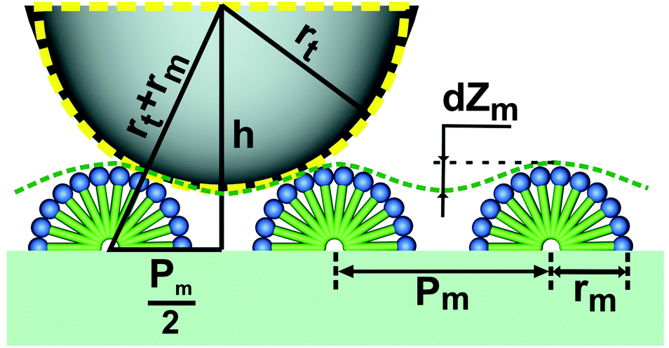 | ||
| Fig. 3 Image of the topographic modulation dZm obtained as a result of scanning the graphite/solution interface created by hemi-cylindrical micelles of radius rm using a hemisphere-like AFM probe of radius rt. | ||
The first direct image of the morphology of CTAB aggregates adsorbed from the aqueous solution on the hydrophobic substrate have been recently obtained using an AFM method.33 The aggregates exist in the form of “hemi-cylindrical half-micelles”, epitaxially oriented along the symmetry axes of the graphite surface. The distance between half-micelles is twice the length of the surfactant molecules. Such aggregates were observed in the concentration range 0.9–5.5 of the critical micelle concentration (CMC). According to modern concepts, at a surfactant concentration below the volume of CMC, amphiphilic molecules are adsorbed substantially, orienting parallel to the surface according to a “head-to-head”/“tail-to-tail” scheme. At higher concentrations (>CMC), semi-cylinders arrange at the phase interface, forming periodic extended structures (strips), separated by a distance approximately equal to twice the length of the surfactant molecules. This structuring of surfactant molecules on the graphite substrates was observed for both types of surfactant – ionic and non-ionic. A key role in controlling the morphology of the aggregates is played by the crystal lattice structure of graphite, which orients the surfactant molecules along the graphite crystallographic directions. The determining criterion in this case was supposed to be the correspondence between the graphite lattice period (0.246 nm) and the length of the methylene link (0.254 nm). An increase in the packing density of hemi-cylinders with an increase in surfactant concentration has also been confirmed.16 So the amplitude of the topographic modulation depends on the surfactant concentration of hemi-cylindrical CTAB micelles at the phase interface of graphite/solution; dZm decreases from 0.7 nm at C = 0.5 CMC to 0.4 nm at C = 10 CMC.
A dependence of the same nature for the surfactant aggregates’ period at the graphite/solution interface on the concentration of sodium dodecyl sulfate (SDS) has also been observed previously.35 The adsorbate period decreased from 7 to 5.2 nm with the increase in SDS concentration from 3 to 100 mM. It has been shown that an increase in concentration of Mg2+ ions leads to a denser packing of hemi-cylindrical micelles36 due to neutralization of the electrostatic repulsion between SDS head groups.
The temperature dependence of the repeat period has a critical nature: in the narrow temperature range of 1–1.5 °C, a steep 2-fold increase in the period is observed.16 Analysis of the interactions contributing to the temperature-induced structural changes gave the basis for introducing a new concept of a transition of the half-cylinders to pre-cylinders with a quantitative ratio of 2![[thin space (1/6-em)]](https://www.rsc.org/images/entities/char_2009.gif) :1.
:1.
In ref. 32, similar hemi-cylindrical micelles from CTAB molecules have already been observed at the glass/solution phase interface; in a narrow temperature range of 28–28.6 °C, an approximate doubling of the repeat period of the strips (from 5 to 11 nm) was observed, i.e., hemi-cylindrical admicelles have been changed to cylindrical ones. It should be noted that the graphite surface is hydrophobic and the glass surface is hydrophilic (Table 1). In the case of the glass substrate, there are also no specific crystallographic axes with a distance between them that could be comparable to the length of the methylene link. However, it should be noted that the value of the glass surface dispersity is 5 nm (ref. 32) – approximately twice the length of the methylene link.
| No | Substrate | CA(M) [°] | CA(L) [°] | CA(R) [°] | WoA [mN cm−1] | Hydrophilic (90−) or hydrophobic (90+) properties |
|---|---|---|---|---|---|---|
| CA(M) is average contact angle, CA(L) and CA(R) are left and right contact angles, respectively, WoA is work of adhesion. | ||||||
| 1 | HOPG | 96.05 | 96.47 | 95.62 | 65.87 | HPB |
| 2 | Glass | 45.31 | 46.98 | 43.65 | 122.78 | HPL |
Measurement of the curvature radius of the probe tip
The radius of the probe tip can be estimated by measuring the topographic modulation during scanning of the micelles. According to Fig. 3, the following equations are valid:| h = rt + rm − dZm, | (1) |
| (rt + rm)2 = h2 + (Pm/2)2. | (2) |
A solution of the system of eqn (1 and 2) in relation to rt is
| rt = dZm/2 + Pm2/8 dZm − rm. |
By substituting dZm ∼ 0.7 nm and Pm ∼ 7.5 nm from Fig. 3, a value for the curvature radius of the probe tip rt ∼ 10 nm was obtained. This corresponds to a value of 10–13 nm declared by the manufacturer.
Palladium nanolattice on HOPG
Fig. 4A shows the AFM contact mode image of the Pd self-assemblies on the surface of atomically smooth HOPG obtained using chemical deposition in a liquid medium at 25 °C with the aid of a surface micellar template. The template was formed by CTAB aggregates and later rinsed off after the synthesis was complete. Fig. 4 shows parallel matrices of linear chains of Pd nanoparticles with a sufficiently long length (several tens of microns) compared with the width (∼40 nm). It should be noted that the nanoparticles are randomly arranged on part (nearly 30%) of the surface of the same sample, predominantly at the edge of the Pd substrate (ESI†). Perhaps this is due to the inhomogeneity of the surface properties of the substrate at the edges and near the center.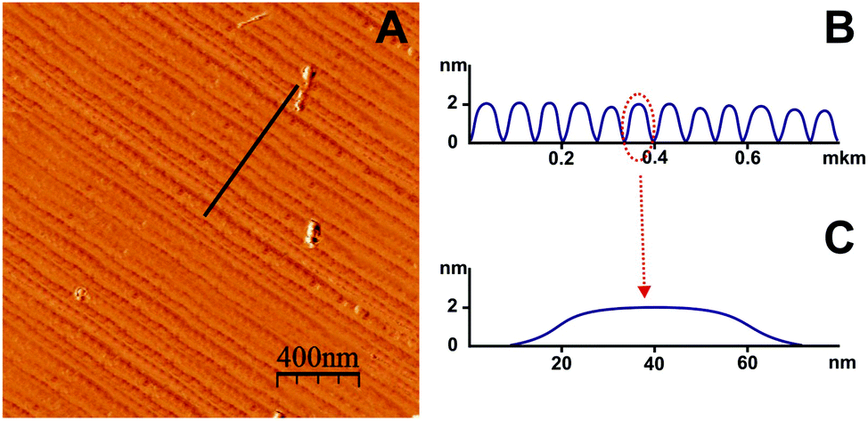 | ||
| Fig. 4 AFM contact mode image of the Pd self-assemblies on the surface of atomically smooth HOPG at 25 °C (A), topographic modulation of the probe tip position in the vertical direction along the black line (B), and profile of one of the strips (C). | ||
The cross-sectional shape and arrangement of the palladium strips are very different from those of the platinum strips.16 Palladium spreads better over the hydrophobic surface of HOPG and has a contact angle less than an order of magnitude than platinum has in the same conditions. The palladium strips lie close to each other and are almost in contact, while the distance between the platinum strips is nearly 100 nm. Despite these inherent differences, it is necessary to emphasize the universality of the developed method to obtain one-dimensional nanostructures of precious metals on a solid surface.
For the synthesis of parallel Pd strips on a graphite surface, a drop of 1 mM CTAB solution and 0.1 mM PdCl2 solution in water was applied to the clean surface of HOPG in the liquid cell.
Surface admicelles were formed over the next 30 minutes. Then, Pd2+ ions were reduced with 5 mM hydrazine solution over 1 h. Then, surface micelles were removed from the surface by washing with water and ethanol and the fluid cell was dried at 40 °C for 4 h.
The elemental composition of the material deposited on the surface of HOPG was analyzed using X-ray fluorescence spectroscopy. According to the characteristic lines at 21.12 (Kα) and 23.80 (Kβ) keV in Fig. 5, it can be concluded that the material contains Pd particles. There were no characteristic lines of bromine at 11.91 keV (Kα) and 13.29 keV (Kβ) indicating the absence of CTAB molecules containing Br ions.
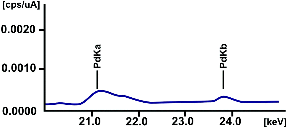 | ||
| Fig. 5 X-ray fluorescence spectrum of the substrate surface with the deposited material at 25 °C. | ||
To investigate Pd using TEM, the metal was deposited on the surface of copper grids (300 mesh) covered with a formvar membrane. The deposition occurred using the method mentioned above. During the deposition of Pd on formvar, separate metal particles were obtained instead of an arranged system of metal strips. The sizes of the particles are 2–5 nm (Fig. 6). The properties of the formvar surface significantly differ from the properties of the HOPG surface. This fact did not allow arranged metal strips to be formed. However, the elemental composition of the deposited material was confirmed. In Fig. 7 the EDX spectrum relating to the TEM image area (Fig. 6) is shown. Two lines of Pd (Mζ = 0.286 kV, Mγ = 0.532 kV) are clearly seen in the spectrum. Lines of carbon, silica and copper are also seen in the spectrum. These lines correspond to the substrate.37 In addition, the lack of bromine lines in the spectrum confirms that other components of the reaction are not included in the obtained product.
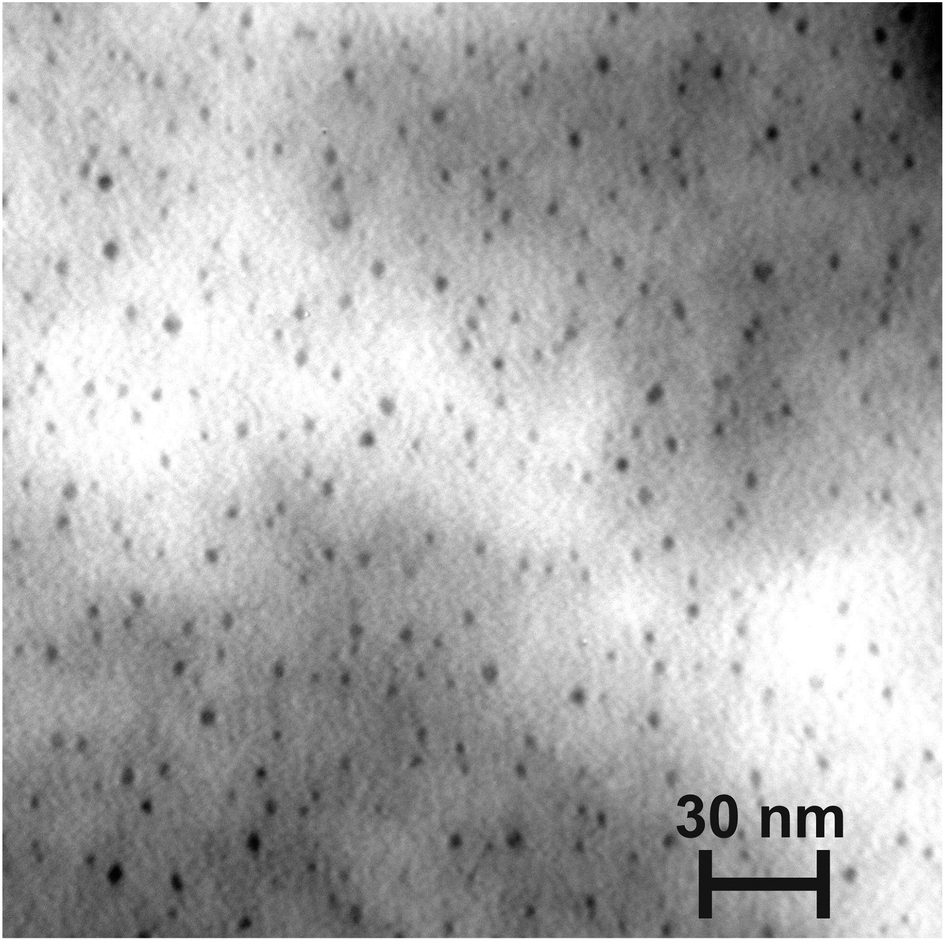 | ||
| Fig. 6 TEM image of Pd particles deposited on the surface of formvar using CTAB micellar template. | ||
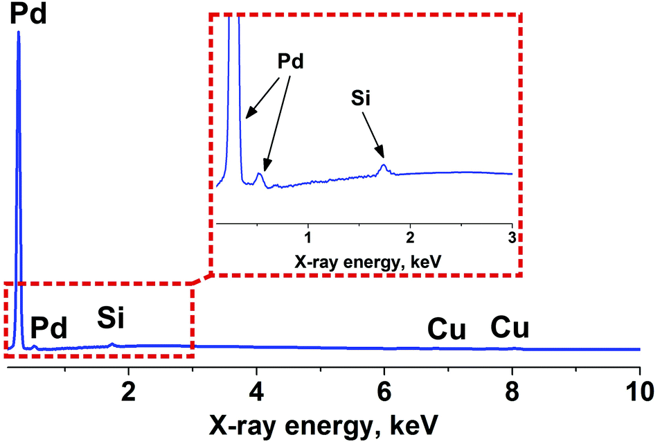 | ||
| Fig. 7 Spectrum of TEM-EDX analysis of Pd particles deposited on the surface of formvar using CTAB micellar template. | ||
The diagnostic curves of MEA with a surface density of Pd of 0.5 mg cm−2 on both the anode and cathode sides in an H2/O2 fuel cell are shown in Fig. 8. The curve of the dependence of the power density on the current density shows that a maximum power density of 2.4 mW cm−2 is achieved at a current density of 11 mA cm2. These data confirm that the precipitated strips are composed of metallic palladium.
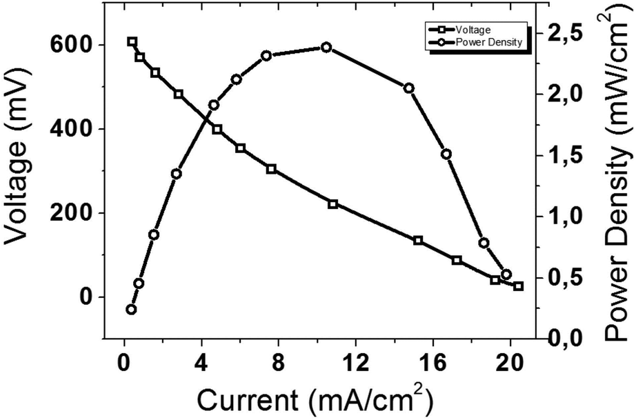 | ||
| Fig. 8 Diagnostic curves of the MEA with a surface density of Pd of 0.5 mg cm−2 in an H2/O2 fuel cell. | ||
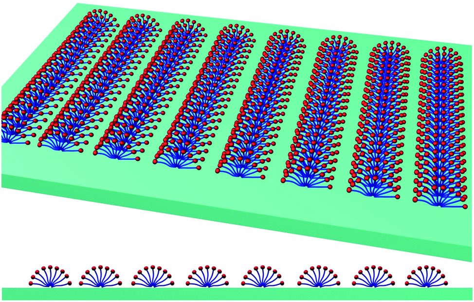
The template directed sintering process of Pd nanoparticles mediated by surface micelles (Fig. 9A) could be divided into several stages. During chemical reduction, individual Pd nanoparticles are formed through nucleation along the long axis of the surface micelles (Fig. 9B) and then linked together into linear chains oriented in the same direction, as schematically shown in Fig. 9C. Particle growth will occur between the admicelles. After washing off the template from the surface micelles, coalescence of several (about 9 in this case) neighboring Pd linear chains into a broader strip of Pd (Fig. 9D) was observed. The height of the strips is 2 nm, the width is 40 nm and the repeat period is 67 nm (according to Fig. 4).
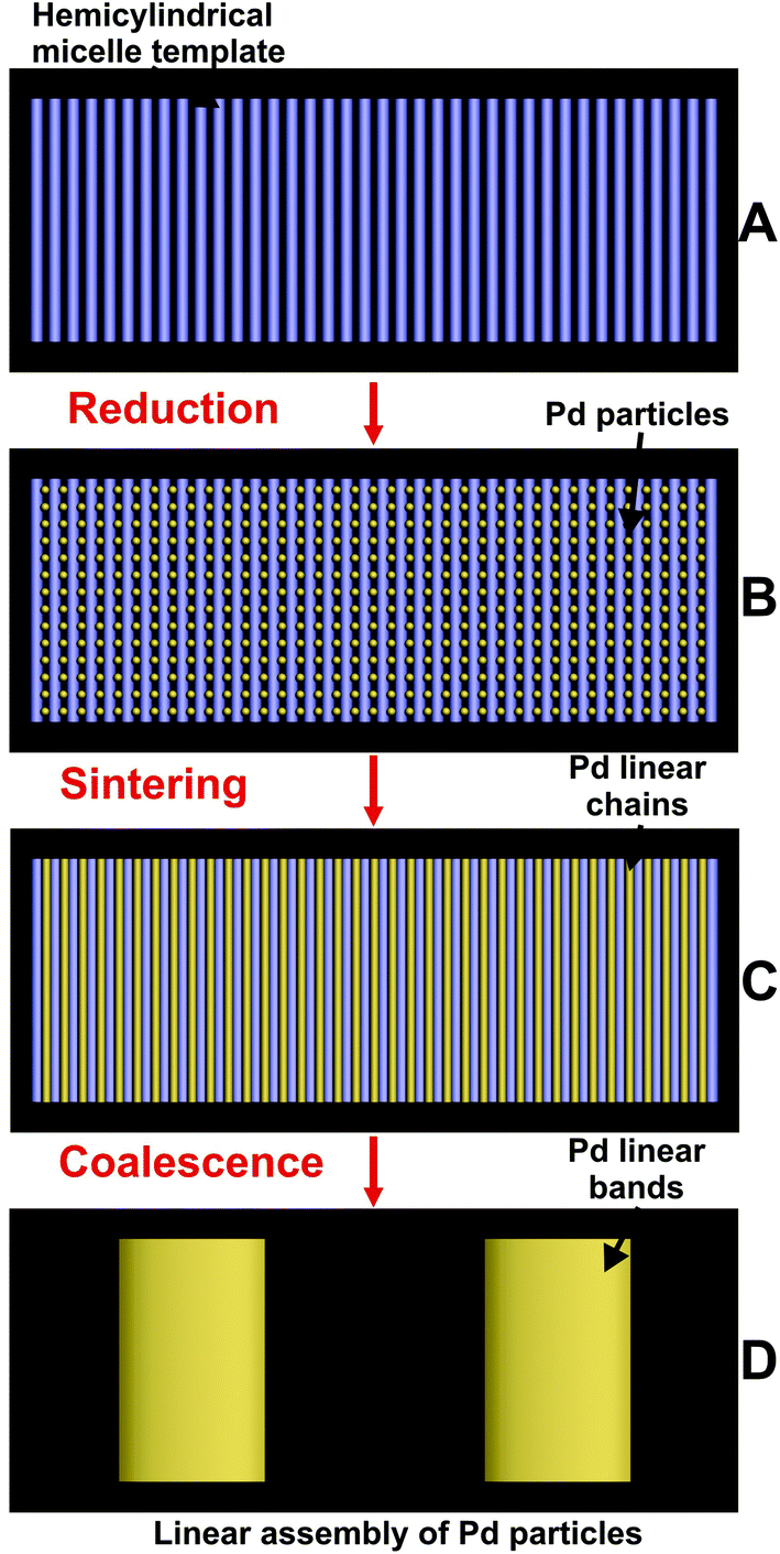 | ||
| Fig. 9 Illustration of the mechanism of formation of Pd strips using a micellar template. | ||
Conclusions
The method16,32 of synthesis of linear nanoclusters of noble metals on a solid support was expanded to produce a palladium lattice. The morphological characteristics of the linear clusters (the repeat period of the Pd strips is 65 nm, width 40 nm and height 2 nm) are attractive for nanotechnology applications. The elemental composition of the metal clusters was confirmed using X-ray fluorescence and TEM-EDX methods. The fact that the strips are composed of metallic Pd was also confirmed by testing the membrane electrode assembly with the strips in a commercial fuel cell. The work is attractive because it describes a quick and cheap method for the synthesis of a nanoscale Pd lattice on a solid support.Acknowledgements
Financial support from the Russian Foundation for Basic Research (grant no. 14-03-00258A) is greatly appreciated.References
- G. Kartopu and O. Yalçın, Electrodeposited Nanowires Their Appl., 2010, 228, 113–140 Search PubMed.
- T. Ahmadi, Z. Wang, T. Green, A. Henglein and M. El-Sayed, Science, 1996, 272, 1924–1925 CrossRef CAS PubMed.
- T. Ahmadi, Z. Wang, A. Henglein and M. El-Sayed, Chem. Mater., 1996, 8, 1161–1163 CrossRef CAS.
- N. Melosh, A. Boukai, F. Diana, B. Gerardot, A. Badolato, P. Petroff and J. Heath, Science, 2003, 300, 112–115 CrossRef CAS PubMed.
- Y.-J. Han, J. Kim and G. Stucky, Chem. Mater., 2000, 12, 2068–2069 CrossRef CAS.
- J. Shui and J. Li, Nano Lett., 2009, 9, 1307–1314 CrossRef CAS PubMed.
- M. Shirai, K. Igeta and M. Arai, Chem. Commun., 2000, 623–624 RSC.
- D. Lee, J. Choung, Y. Pyun, K. Son and W. Park, 3rd International Nanoelectronics Conference. Book of Abstracts, 2010, pp. 1282–1283.
- W. Wu and L. Wang, Nano Lett., 2011, 11, 2779–2785 CrossRef CAS PubMed.
- G. Kartopu, S. Habouti and M. Es-Souni, Mater. Chem. Phys., 2008, 107, 226–230 CrossRef CAS.
- L. Piraux, S. Dubois, A. Fert and L. Belliard, Eur. Phys. J. B, 1998, 4, 413–420 CrossRef CAS.
- D. Strukov, D. Snider, D. Stewart and R. Williams, Nature, 2008, 453, 80–83 CrossRef CAS PubMed.
- L. Chua, IEEE Trans. Circuit Theory, 1971, 18, 507–519 CrossRef.
- H. Kawasaki, M. Uota, T. Yoshimura, D. Fujikawa, G. Sakai, M. Annaka and T. Kijima, Langmuir, 2005, 21, 11468–11473 CrossRef CAS PubMed.
- H. Kawasaki, M. Uota, T. Yoshimura, D. Fujikawa, G. Sakai and T. Kijima, Colloid Interface Sci., 2006, 300, 149–154 CrossRef CAS PubMed.
- M. Kadirov, I. Nizameev and L. Zakharova, J. Phys. Chem. C, 2012, 116, 11326–11335 CrossRef CAS.
- M. Kadirov, A. Bosnjakovic and S. Schlick, J. Phys. Chem. B, 2005, 109, 7664–7670 CrossRef CAS PubMed.
- M. Danilczuk, A. Bosnjakovic, M. Kadirov and S. Schlick, J. Power Sources, 2007, 172, 78–82 CrossRef CAS.
- A. Bosnjakovic, M. Kadirov and S. Schlick, Res. Chem. Intermed., 2007, 33, 677–687 CrossRef CAS.
- T. Pashirova, E. Zhil'tsova, R. Kashapov, S. Lukashenko, A. Litvinov, M. Kadirov, L. Zakharova and A. Konovalov, Russ. Chem. Bull., 2011, 59, 1745–1752 CrossRef.
- L. Zakharova, Y. Kudryashova, N. Selivanova, M. Voronin, A. Ibragimova, S. Solovieva, A. Gubaidullin, A. Litvinov, I. Nizameev and M. Kadirov, et al. , J. Membr. Sci., 2010, 364, 90–101 CrossRef CAS.
- M. Kadirov, Yu. Budnikova, T. Gryaznova, O. Sinyashin, M. Bubnov, A. Krashilina and V. Cherkasov, Russ. Chem. Bull., 2007, 56, 104–107 CrossRef CAS.
- M. Kadirov, E. Tretyakov, Y. Budnikova, M. Valitov, K. Holin, T. Gryaznova, V. Ovcharenko and O. Sinyashin, J. Electroanal. Chem., 2008, 624, 69–72 CrossRef CAS.
- Y. Budnikova, T. Gryaznova, M. Kadirov, E. Tret'yakov, K. Kholin, V. Ovcharenko, R. Sagdeev and O. Sinyashin, Russ. J. Phys. Chem. A, 2009, 83, 1976–1980 CrossRef CAS.
- M. Kadirov, E. Tret'yakov, Y. Budnikova, K. Kholin, M. Valitov, V. Vavilova, V. Ovcharenko, R. Sagdeev and O. Sinyashin, Russ. J. Phys. Chem. A, 2009, 83, 2163–2169 CrossRef CAS.
- M. Kadirov, Y. Budnikova, K. Kholin, M. Valitov, S. Krasnov, T. Gryaznova and O. Sinyashin, Russ. Chem. Bull., 2010, 59, 466–468 CrossRef CAS.
- J. Ciszewski, D. Mikhaylov, K. Holin, M. Kadirov, Y. Budnikova, O. Sinyashin and D. Vicic, Inorg. Chem., 2011, 50, 8630–8635 CrossRef CAS PubMed.
- R. Galimullina, M. Valitov, Y. Spiridonova, E. Musina, S. Krasnov, M. Kadirov, A. Karasik, Y. Budnikova and O. Sinyashin, Russ. J. Phys. Chem. A, 2011, 85, 2214–2221 CrossRef CAS.
- M. Kadirov, K. Kholin, E. Tselishcheva, V. Burilov and A. Mustafina, Russ. Chem. Bull., 2013, 62, 1327–1331 CrossRef CAS.
- K. Kholin, M. Valitov, V. Burilov, E. Tselischeva, S. Strekalova, A. Mustafina, Yu. Budnikova and M. Kadirov, Electrochim. Acta, 2015, 182, 212–216 CrossRef CAS.
- Y. Wang, D. Lu, H. Yan and R. Thomas, J. Phys. Chem. B, 1997, 101, 3953–3956 CrossRef CAS.
- M. Kadirov, A. Litvinov, I. Nizameev and L. Zakharova, J. Phys. Chem. C, 2014, 118, 19785–19794 CrossRef CAS.
- L. Zook and J. Leddy, Anal. Chem., 1996, 68, 3793–3796 CrossRef CAS PubMed.
- S. Manne, J. Cleveland, H. Gaub, G. Stucky and P. Hansma, Langmuir, 1994, 10, 4409–4413 CrossRef CAS.
- E. Wanless and W. Ducker, J. Phys. Chem., 1996, 100, 3207–3214 CrossRef CAS.
- E. Wanless and W. Ducker, Langmuir, 1997, 13, 1463–1474 CrossRef CAS.
- J. V. Niemi and S. Saarikoski, Atmos. Chem. Phys. Discuss., 2006, 6, 6753–6799 CrossRef.
Footnote |
| † Electronic supplementary information (ESI) available: AFM images of palladium on HOPG surface, AFM images of the structure of CTAB at the graphite-water interface. See DOI: 10.1039/c6dt01234e |
| This journal is © The Royal Society of Chemistry 2016 |