DOI:
10.1039/C5DT04920B
(Paper)
Dalton Trans., 2016,
45, 3506-3521
Synthesis and characterization of DNA fenced, self-assembled SnO2 nano-assemblies for supercapacitor applications
Received
17th December 2015
, Accepted 6th January 2016
First published on 7th January 2016
Abstract
Self-assembled, aggregated, chain-like SnO2 nano-assemblies were synthesized at room temperature by a simple wet chemical route within an hour in the presence of DNA as a scaffold. The average size of the SnO2 particles and the chain diameter were controlled by tuning the DNA to Sn(II) molar ratio and altering the other reaction parameters. A formation and growth mechanism of the SnO2 NPs on DNA is discussed. The SnO2 chain-like assemblies were utilized as potential anode materials in an electrochemical supercapacitor. From the supercapacitor study, it was found that the SnO2 nanomaterials showed different specific capacitance (Cs) values depending on varying chain-like morphologies and the order of Cs values was: chain-like (small size) > chain-like (large size). The highest Cs of 209 F g−1 at a scan rate of 5 mV s−1 was observed for SnO2 nano-assemblies having chain-like structure with a smaller size. The long term cycling stability study of a chain-like SnO2 electrode was found to be stable and retained ca. 71% of the initial specific capacitance, even after 5000 cycles. A supercapacitor study revealed that both morphologies can be used as a potential anode material and the best efficiency was observed for small sized chain-like morphology which is due to their higher BET surface area and specific structural orientation. The proposed route, by virtue of its simplicity and being environmentally benign, might become a future promising candidate for further processing, assembly, and practical application of other oxide based nanostructure materials.
Introduction
In recent years, interest in the fabrication of one-dimensional (1-D) semiconductor materials has attracted great research attention because of their potential importance in fundamental research and in technological perspectives. Considerable attention has been made to construct 1D semiconducting materials using a variety of nanofabrication techniques and crystal growth mechanisms. Template-based synthesis of 1-D nano-assemblies is an elegant chemical approach for the fabrication of nanostructures.1,2 At nanoscale, materials show intrinsic properties that are governed by their size, shape, and structures. Careful literature investigation revealed that the study of metal nanomaterials is more comparable to semiconductor metal oxides. Hence, considerable attention has been devoted to a ‘bottom-up’ method where molecular components are self-assembled into a complex structure. Therefore, it is quite reasonable to determine a suitable route for the synthesis of 1-D self-assembled nanomaterials in a short time scale and in an easy manner. Among the different oxide materials studied so far, tin dioxide (SnO2), particularly was found to be more interesting and have many important applications.3–8 SnO2 is a n-type semiconductor with a large band gap (Eg = 3.6 eV at 300 K), which finds wide application in gas sensors,3 dye sensitized solar cells (DSSC),4,5 catalysis reactions,6 Li-ion batteries,7 and as a suitable electrode material in electrochemical supercapcitors.8
Different morphologies of low dimensional SnO2 nanostructures have been reported (like zero dimensional nanoparticles (NPs),9 1-D nanorods,10 nanobelts,11 nanowires,12 nanotubes,13 and two-dimensional (2-D) nanosheets14). Moreover, recently a three-dimensional (3-D) hierarchical architecture has also been reported by a few researchers.15,16 Additionally, doping of SnO2 based nanomaterials offers a convenient way to tailor their electrical, structural, and optical properties. Therefore, development of suitable synthetic strategies is crucial for providing desired property control. Different types of bio-molecules such as proteins, peptides, and amino acids can be used as scaffolds, templates, and stabilizers for the formation of metal, hybrid, and composite nanomaterials with unique properties.17–19 Among the different bio-molecules, deoxyribonucleic acid (DNA) has been used widely as a biological template to build nanostructures with specific morphologies.20,21 DNA strands offered a variety of binding sites for several metal ions and stands to be an ideal candidate for programming the self-assembly of nanomaterials into 1-D structures.22–24 In DNA structures, mainly two binding sites are available. The first one is the negatively charged phosphate group and another one is the aromatic base molecules. A few other important properties of DNA are: (i) a double helix structure with better mechanical strength; (ii) intermolecular interactions in DNA can be readily programmed and reliably predicted; and (iii) the versatile chemical structure allowed DNA to self-assemble into complex structure-like cubes, squares, etc.25–28 The backbone of DNA, made of phosphate and sugar molecules, can bind with various metal cations and metal NPs via electrostatic interactions. Therefore, within the past few years, a growing number of researchers have been paying attention to using DNA as “smart materials” to direct the assembly of inorganic materials.
As discussed before, SnO2 nanomaterials can be used widely in DSSC and as electrode materials in electrochemical supercapacitor studies.4,5,7,8 It is well-known that SnO2 acquires a special place because of its lower cost and environmentally benign nature. Similarly, different oxide materials like MnO2,29 TiO2,30 and RuO2![[thin space (1/6-em)]](https://www.rsc.org/images/entities/char_2009.gif) 31 have been used as electrode materials for supercapacitors because of their large capacitance and fast redox kinetics. However, to reduce the cost factor, alternative oxides were investigated. A SnO2 composite with polyaniline (PANI) showed good supercapacitive activity.
31 have been used as electrode materials for supercapacitors because of their large capacitance and fast redox kinetics. However, to reduce the cost factor, alternative oxides were investigated. A SnO2 composite with polyaniline (PANI) showed good supercapacitive activity.
Different routes have been employed for the synthesis of SnO2 nanomaterials. Sunkara et al. synthesized SnO2 nanowires on a quartz substrate and observed a DSSC efficiency of 2.1%.32 Qiao et al. prepared an urchin-like SnO2 microstructure and coated it with thin layers of TiO2 for their application in DSSC.33 Zhang et al. prepared a PANI–SnO2 composite for supercapacitor applications.34 Wang et al. prepared single crystalline SnO2 nanorod arrays using hydrothermal routes and observed a DSSC efficiency <0.4%.35 Xie et al. prepared SnO2 nanotubes and SnO2–TiO2 core shell nanomaterials for DSSC applications.36 They observed that bare SnO2 gave efficiency ∼0.99% whereas SnO2–TiO2 composites gave efficiency of 5.11%. Tremel et al. synthesized SnO2 nanocrystals by a microwave-based hydrothermal route and used them in DSSC applications.37 There are a few other reports where SnO2 nanomaterials were synthesized using different routes and then applied as a battery material or in a photocatalytic reaction.38,39 Most of the above reports on SnO2 nanomaterials required a long reaction time, high temperature, very expensive reagents, or generated particles with various morphologies. So, we investigated an easy route with a low temperature reaction and uniform particle morphology for the synthesis of SnO2 nanomaterials. To the best of our knowledge, there is no information available for the formation of aggregated, chain-like SnO2 nano-assemblies on a DNA scaffold within 1 h of reaction time at room temperature. The chain-like SnO2 nano-assemblies on DNA show potential applications in electrochemical supercapacitors and in DSSC studies.
In this article we synthesized aggregated, chain-like SnO2 nano-assemblies on a DNA scaffold at room temperature with 40 min of reaction time. SnO2 nano-chains were synthesized by the reaction of SnCl2 and water in the presence of DNA under continuous stirring. The small size SnO2 particles are self-assembled, aggregated, and grown on DNA with a chain-like morphology. The size of the individual SnO2 particles, diameter, and length of the chains was tuned by altering the DNA with SnCl2 molar ratio and controlling other reaction parameters. The SnO2 chain-like assemblies were utilized as potential anode materials in electrochemical supercapacitors. From electrochemical supercapacitor studies, it was found that SnO2 nano-assemblies showed different specific capacitance (Cs) values for various nano-chains and the order of Cs values were as follows: chain-like (small size) > chain-like (large size). A long term cycling stability study of a chain-like SnO2 electrode showed it to be stable and retaining a Cs value 71% of its initial specific capacitance, even after 5000 consecutive cycles. The supercapacitor study revealed that both of the morphologies can be used as a potential anode material and the best efficiency was observed for small size chain-like morphology which is due to their higher BET surface area and specific structural orientation. In the future, the proposed route, by virtue of its simplicity and being environmentally benign, might become a promising candidate for further processing, assemblies, and practical applications for other oxide-based nanostructure materials.
Experimental section
Reagents
DNA (double-stranded herring testes) with an average molecular weight ∼50 K bp (base pair) was purchased from Sigma-Aldrich. The Sn(II) chloride (SnCl2) salt was obtained from Sigma-Aldrich and used as received. Absolute ethyl alcohol (CH3CH2OH) was obtained from Changshu Yangyuan Chemical from China. N-Methyl-2-pyrrolidone (NMP), acetylene black was purchased from Sigma-Aldrich and used as received. Nickel foam and polyvinylidene fluoride (PVDF) were obtained from Alfa Aesar. De-ionized (DI) water was used for the entire synthesis and application purposes.
Instruments
The synthesized chain-like SnO2 nano-assemblies on DNA scaffolds were characterized using several spectroscopic techniques. Transmission electron microscopy (TEM) and high resolution transmission electron microscopy (HR-TEM) analysis was done with a Tecnai model TEM instrument (TecnaiTM G2 F20, FEI) with an accelerating voltage of 200 KV. The UV-Visible (UV-Vis) absorption spectra were recorded with a Unico (model 4802) UV-Vis-NIR spectrophotometer equipped with a 1 cm quartz cuvette holder for liquid samples. Energy Dispersive X-ray Spectroscopy (EDS) analysis was done with a Field Emission Scanning Electron Microscopy (FE-SEM) instrument (Zeiss ultra FE-SEM instruments) with a separate EDS detector (INCA) connected to it. X-ray diffraction (XRD) analysis was done using a PAN analytical Advanced Bragg-Brentano X-ray powder diffractometer (XRD) with Cu Kα radiation (λ = 0.154 nm) with a scanning rate of 7 degree per min in the 2θ range 10–90°. The photoluminescence (PL) study was done with a Varian (Cary Eclipse Winflr) fluorescence spectrophotometer (serial number el02045776), both in excitation and emission modes, using a xenon pump lamp. Fourier Transform Infrared (FT-IR) spectroscopy analysis was done with the model Nexus 670 (FTIR), Centaurms 10× (Microscope) having a spectral Range of 4000 to 400 cm−1 with a MCT-B detector. The thermal analysis study was recorded with a thermal analyser-simultaneous TGA/DTA instrument with model name SDT Q600 and the analysis was performed in air. A hot air oven (temperature up to 1000 °C) was used to anneal the samples at a specific temperature. All the electrochemical experiments were examined using an AUTOLAB PGSTAT302N electrochemical work station in a 2 M KOH aqueous solution.
Synthesis of self-assembled, aggregated chain-like SnO2 nano-assemblies on DNA scaffold
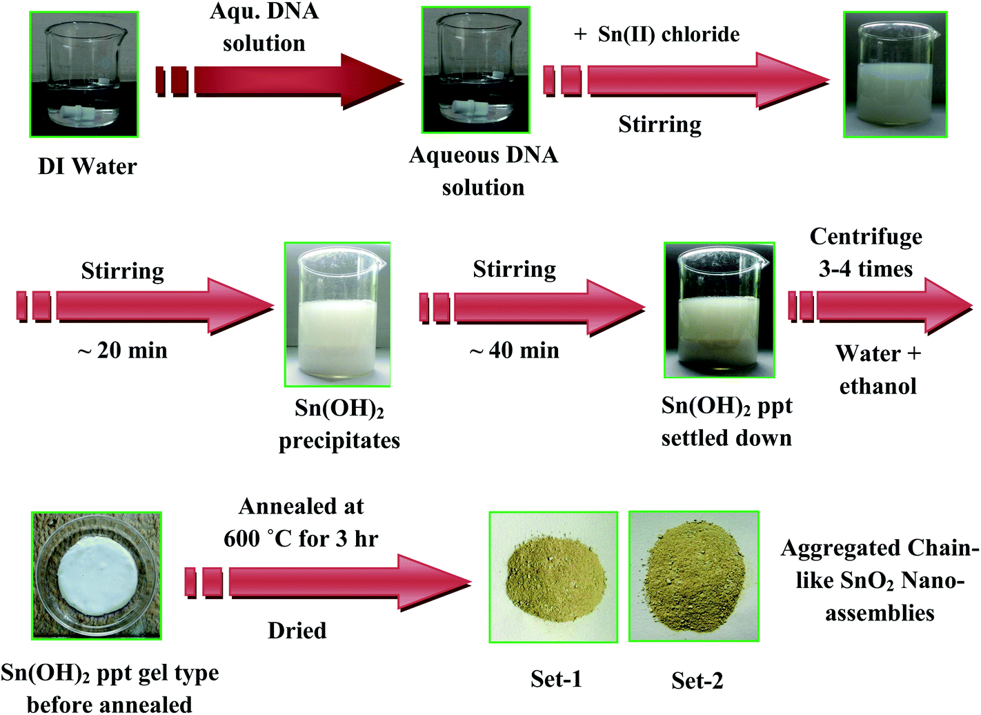
SnO2 nano-assemblies having a chain-like morphology can be synthesized by the reaction of SnCl2 aqueous salt solution in the presence of DNA under continuous stirring. For a typical synthesis, 10 mL of DNA solution was mixed with 130 mL of water and stirred for 10 minutes. The solution was colorless at that stage. Next, 200 mL of 0.5(M) Sn(II) salt solution was added drop wise for 10 min with continuous stirring. The colorless solution slowly turned into a milky white turbid solution. The solution was continuously stirred for another 20 min. After 5–10 min, a white sediment settled and it was collected by centrifugation with water and ethanol for 3–4 times. After centrifugation, the white paste-like Sn(OH)2 was heated initially at 60 °C for 1 h and finally annealed at 600 °C for 3 h. The other sets were prepared by varying the concentration of the starting regents. Table 1 shows different final concentrations of all the regents used for the synthesis, total time of reaction, size of the materials, and shape of the particles. Scheme 1 is a schematic representation of the entire synthesis process.
 |
| | Scheme 1 Shows the schematic presentation for the synthesis of DNA–SnO2 nano-assemblies. | |
Table 1 The different final concentrations of all reagents used, size and shape of the particles for the formation of self-assembled, aggregated, chain-like SnO2 nano-assemblies on DNA
| Set no. |
Final conc. of DNA (M) |
Final conc. of SnCl2 salt (M) |
Volume of DI water added (mL) |
Total time of stirring at RT (min) |
Shape of the SnO2 nano-assemblies |
Approx. size of the SnO2 particles (nm) |
Shape distribution |
| 1 |
3.61 × 10⁻³ |
2.94 × 10⁻² |
130 |
40 |
Aggregated chain-like |
Chain diameter 40 ± 5, individual NPs size ∼3.5 ± 0.2 |
100% chain-like |
| 2 |
5.06 × 10⁻² |
2.94 × 10⁻² |
0 |
40 |
Aggregated chain-like |
Chain diameter 100 ± 10, individual NPs size ∼2.0 ± 0.3 |
100% chain-like |
Fabrication of electrodes for electrochemical supercapacitor applications
A working electrode was prepared by mixing the electroactive material, acetylene black and polyvinylidene fluoride (PVDF) with a mass ratio of 80:10:10 in N-methyl-2-pyrrolidone to form a homogeneous slurry. Then the slurry was coated on the nickel foam current collector (area = 1 cm × 1 cm) and dried at 90 °C for 24 h to evaporate the solvent. The loading mass of the electroactive material was about 7 mg cm−2. Electrochemical measurements were carried out using a standard three electrode system with 2 M KOH aqueous solution. A platinum sheet and Hg/HgO were used as the counter and reference electrode, respectively. Cyclic voltammetry (CV) tests were performed at various scan rates within a potential range of 0 to 0.6 V. Galvanostatic charge–discharge (CD) measurements were carried out in the potential range from 0 to 0.55 V at a current density of 0.5, 1, 2, 3, 4, 5, and 7.5 A g−1. Electrochemical impedance spectroscopy (EIS) tests were conducted over the frequency range of 100 kHz to 10 mHz with an AC amplitude of 5 mV at open circuit potential. The specific capacitances of the SnO2 electrodes were calculated from the CV and GCD curves, according to the following equations:29,40| |  | (1) |
| |  | (2) |
where, Cs is the specific capacitance (F g−1),  is the integrated area under the CV curve (A), v is the scan rate (mV s−1), m is the mass of the electroactive material (g), ΔV is the potential window (V), I is the discharge current (A), and Δt is the discharge time (s).
Preparation of samples for different other characterizations
The chain-like SnO2 nano-assemblies on a DNA scaffold were characterized using UV-Vis, TEM, EDS, XRD, photoluminescence (PL), LASER-Raman, FT-IR, and thermal analysis. The SnO2 nano-assemblies solution, after successive centrifugation and annealing, was used for measurements in a UV-Vis spectrophotometer after dispersing in an aqueous solution. The solid SnO2 powder was mixed with DI water, sonicated for 20 min and used for TEM sample preparation and other thin film preparations. The dispersed SnO2 nanostructures in aqueous solution were used for the PL measurements. Samples for TEM were prepared by placing a drop of the corresponding SnO2 NPs solution onto a carbon coated Cu grid followed by slow evaporation of solvent at ambient conditions. For EDS, XRD, Laser Raman, and FT-IR analysis, glass slides were used as substrates for thin film preparation. The slides were cleaned thoroughly in acetone and sonicated for about 20 min. The cleaned substrates were covered with the SnO2 nanostructures solution and then dried in air. After the first layer was deposited, subsequent layers were deposited by repeatedly adding more SnO2 nanostructures solution and drying. Final samples were obtained after 5–6 times depositions and then analyzed using the above techniques. For TGA/DTA analysis, the as prepared DNA–SnO2 nano powders were directly used for the measurements. The sample preparation for a supercapacitor application is given in a later section under the experimental part.
Results and discussion
UV-Vis spectroscopic study
Fig. 1A shows the room temperature UV-Visible (UV-Vis) spectra of different solution mixtures for the formation of self-assembled chain-like SnO2 nano-assemblies on a DNA scaffold. Curve a, Fig. 1A shows the absorption band of only aqueous DNA solution which has a peak maxima at 258 nm due to absorption of aromatic base molecules. Curve b (Fig. 1A) shows the absorption band of only aqueous Sn(II) chloride solution and an absorption hump near 282 nm is observed due to ligand to metal charge transfer (LMCT) spectra. Similar types of LMCT bands were observed for other metal salts like Au and Mn.21,29Fig. 1A, curve c shows the absorption band of a mixture of aqueous DNA and aqueous Sn(II) salt, where the absorption hump of Sn(II) salt is not visible although the DNA peak is observed with few nm shifts than the original position. This is due to absorption of oppositely charged Sn+2 ions in DNA. Curve d and e in Fig. 1A show the excitonic absorption band of SnO2 for chain-like (large size) and chain like (small size) nano-assemblies, respectively. From both spectra, we observed a strong peak and, in addition, a small absorption hump at a lower wavelength side below 300 nm. Similar types of UV-Vis absorption bands were observed earlier by Yuan et al.41 and Han et al.42 from their studies on SnO2 nanomaterials. Shifting of absorption hump position for both the morphologies is probably due to the change in particle diameter as discussed in the TEM and FE-SEM analysis section below. Apart from this, we also measured the excitonic transition of SnO2 samples to calculate the band gap energies as shown in Fig. 1B. The theoretical expression determination of band gap via Tauc plot is given elsewhere.43 From the mathematical expression in the Tauc equation, a plot of (αEp)2versus Ep based on a direct transition and the extrapolated value of Ep at α = 0 gives the band gap of SnO2 particles. In the equation α is the absorption coefficient and Ep is the direct photo energy. Curve a and curve b in Fig. 1B show the spectra of SnO2 chain-like morphology having (large size) and SnO2 chain-like morphology having (small size), respectively. The calculated band gap for two different morphologies was 3.46 eV and 3.98 eV, respectively. Compared with the band gap energy of 3.6 eV of SnO2 powder at room temperature, the near band absorption for the SnO2 chain-like nano-assemblies exhibits a blue shift as well as a red shift for the two different morphologies which is ascribed to the size effect of the nanocrystals as reported by others.42 Considering the blue shift and red shift of the two different morphologies compared to bulk SnO2 (band gap ∼3.6 eV), the absorption onset of the synthesis materials can be assigned to the direct transition of electrons in SnO2 nanomaterials.
 |
| | Fig. 1 (A) UV-Visible (UV-Vis) absorption spectra of different solution mixtures for the synthesis of self-assembled, aggregated, chain-like SnO2 nano-assemblies on a DNA scaffold. Curve a shows the absorption spectra of only aqueous DNA solution; curve b shows the absorption band of only aqueous Sn(II) chloride solution; curve c shows the absorption spectrum of the mixture of tin(II) chloride solution with the aqueous DNA solution; curves d and e show the absorption bands of chain-like SnO2 nano-assemblies on DNA with larger and smaller sizes of individual particles respectively. (B) The excitonic transition of SnO2 samples to calculate the band gap energies of chain-like SnO2 nano-assemblies for large size (curve a) and small size (curve b), respectively. | |
Transmission electron microscopy (TEM) and field-emission scanning electron microscopy (FE-SEM) analysis
Transmission Electron Microscopy (TEM) images of the chain-like SnO2 nano-assemblies are shown in Fig. 2. Fig. 2A–D shows the low and high magnified images of the chain-like SnO2 nano-assemblies on DNA having larger sizes. From the images, the average sizes of the individual SnO2 particle are ∼3.5 ± 0.2 nm. The nominal lengths of the chains are ∼1–2 μm. The average chain diameters are ∼40 ± 5 nm. Fig. 2C and D shows the high resolution transmission electron microscopy (HR-TEM) images where lattice fringes are clearly visible. In Fig. 2C, the lattice spacing (d) are 0.26 nm and 0.275 nm and both arise from the (101) lattice plane. Similarly, in Fig. 2D, there are two types of fringes visible where the lattice spacing (d) is 0.264 nm (for 101 plane) and 0.234 nm (for 200 plane), respectively. The inset of Fig. 2D shows the corresponding selected area electron diffraction (SAED) pattern where we did not observe any separate spots either due to small size of the particles or due to their nanocrystalline nature. The ring-type pattern is indexed as (110), (202), (211), and (400) crystal planes of SnO2 nanomaterials. Fig. 2E–H shows the low and high magnified TEM images of the chain-like SnO2 nano-assemblies on a DNA scaffold with small sized particles. Fig. 2E and F is the low magnification image where many chains are assembled to form a network structure (Fig. 2E) and the image of a single nano-chain structure (Fig. 2F). The average individual particles size is calculated to be ∼2.0 ± 0.3 nm whereas the nominal lengths of the chains are ∼1.5–2.5 μm. The average diameters of the chains are ∼100 ± 10 nm. From the image, it is clear that small sized particles are aggregated together to form the chain-like structures. Fig. 2G and H shows the HR-TEM images where lattice fringes are clearly visible. In Fig. 2G, two different crystal planes are visible where the lattice spacing (d) is 0.216 nm (for 211 plane) and 0.34 nm (for 110 plane) respectively. Similarly, in Fig. 2H, there is one type of fringe visible where the lattice spacing (d) is 0.264 nm and arises from the 101 plane. The inset of Fig. 2F shows the corresponding SAED pattern which indicates the particles are crystalline in nature. Although, due to the very small size of the individual particles, we did not observe separate diffraction spots like with single crystal nanomaterials. The ring-type pattern is indexed as (110), (101), (211), and (202) crystal planes of SnO2 nanomaterials. The presence of DNA is visible from all the TEM images and it is clear that the small size SnO2 nano-assemblies are formed initially, then they grow on the DNA chain, aggregate together and generate the chain-like morphologies. Fig. 3A–D shows the FE-SEM images of the chain-like SnO2 nano-assemblies for the different morphologies. Images A–B show the large size SnO2 nano-assemblies at low and high magnification. From the low magnified image it is clear that the formation has an aggregated chain-like morphology and from the high magnified image it is clear that the small particles are assembling together to form the chain-like morphology. The average diameter of the particles and the nominal length of the chains match with the TEM analysis in Fig. 2. Similarly, Fig. 3, image C–D shows the FE-SEM image of the SnO2 chain-like nano-assemblies having smaller sizes. The average size of the SnO2 particles in the nano-chain morphology match with the TEM results as discussed earlier. Therefore, both from TEM and FE-SEM analyses, it is clear that small size SnO2 particles were formed initially, grew on the DNA chain, and then aggregated and self-assembled together and generated the chain-like morphology.
 |
| | Fig. 2 Transmission electron microscopy (TEM) images of the chain-like SnO2 nano-assemblies on a DNA scaffold. A–D show the low and high magnified TEM images having larger size SnO2 nano-assemblies; the inset of D shows the corresponding selected area electron diffraction (SAED) pattern. E–H show the low and high magnified TEM images of the small size SnO2 nano-assemblies; the inset of F shows the corresponding SAED pattern. | |
 |
| | Fig. 3 Low and high magnified FE-SEM images of the large size SnO2 nanomaterials (A–C) and smaller size SnO2 nano-assemblies (B–D) self-assembled to chain-like morphology in DNA. | |
Energy dispersive X-ray spectroscopy (EDS) and X-ray diffraction (XRD) analysis
The energy dispersive X-ray spectroscopic (EDS) analysis of the synthesized DNA–SnO2 nanomaterials is shown in Fig. 4A. The EDS spectrum consists of the different peaks for Sn, Cl, P, O, N, and C. The intense Sn and O peaks came from the SnO2 nano-assemblies while the N, P, and C peaks came from the DNA which is used during the synthesis and confirms its presence in the synthesized product. The Cl peak came from the Sn(II) chloride salt used during the synthesis. Fig. 4B shows the X-ray diffraction (XRD) pattern of the synthesized DNA–SnO2 nano-assemblies after annealing the sample at 600 °C. Curves a and b indicate the XRD pattern of the DNA–SnO2 chain-like morphology as having small size and large size particles. In both of the patterns, the diffraction peak originates from (110), (101), (200), (211), (220), (002), (310), (112), (202), (321), and (400) planes, respectively. The XRD was analyzed in the 2θ range from 10 to 90°. In both curves a and b we observed similar types of XRD patterns. All the above diffraction peaks match well with the standard data file of the SnO2 having JCPDS file no. 41-1445 and can be straightforwardly indexed to the tetragonal rutile phase (P42/mnm) of SnO2.35,36,41,42 No peaks for the other phases of SnO2 were detected, clearly indicating the high purity of the synthesized product. Wang et al. and Han et al. observed exactly similar types of XRD patterns from their synthesis of SnO2 nanomaterials.35,41
 |
| | Fig. 4 (A) Energy dispersive X ray spectroscopy (EDS) analysis of DNA–SnO2 nano-assemblies; the spectrum consists of peaks for Sn, O, P, N, Cl, and C. (B) X-ray diffraction (XRD) pattern of the two different morphologies (curve a, small size and curve b, large size) of the SnO2 nano-assemblies with DNA respectively. | |
Photoluminescence (PL) study
Fig. 5 shows the room temperature photoluminescence (PL) emission spectra of the SnO2 nano-assemblies. In PL, after light excitation by a photon, the electron hole pair might recombine and the recombination rate is closely related to the electronic and the crystal structure. For SnO2 nano-assemblies, the excitation spectrum (not shown here) was used to identify the excitation wavelength at which maximum emission takes place. From the excitation spectra it was found that, at an excitation wavelength of 230 nm, maximum emission takes place. Curve a and curve b in Fig. 5 show the PL emission spectra of chain-like SnO2 nano-assemblies having large and small sizes, respectively. In both of these cases, we observed similar types of absorption spectra as expected. The emission bands are located at 426 nm, 487 nm and 521 nm, respectively. It was reported that SnO2 thin films exhibited a broad dominant peak at 396 nm. In our study, all the emission maxima are located at a higher wavelength side compared to an earlier report by Gu et al.41 signifying that the visible emission cannot be assigned to the direct recombination of a conduction electron in the Sn 4p band and a hole in the O 2p valance band. The highest intense peak at 426 nm might be due to the luminescence centers formed by such tin interstitials or from dangling in the SnO2 nano-assemblies. The other emission band at the higher wavelength side at 487 nm and 521 nm is broad and less intense, probably due to electron transition mediated by defect levels in the band gap such as oxygen vacancies. So, we believe that, in our present SnO2 nanomaterials, the intrinsic defects such as oxygen vacancy act as luminescence centers and can form defect levels located high in the gap, trapping an electron from the valance band to make a contribution to the photoluminescence.
 |
| | Fig. 5 The photoluminescence (PL) emission spectra of SnO2 nano-assemblies on DNA with an excitation wavelength at 230 nm. Curve a and curve b indicate the emission spectra of chain-like SnO2 nano-assemblies with large and small sizes, respectively. | |
Thermal analysis study
Fig. 6 shows the thermo gravimetric analysis (TGA) and differential thermal analysis (DTA) which are used to identify thermal stability and the crystalline condition of the DNA–SnO2 nano-assemblies. The as-synthesized SnO2 nano-assemblies were heated from RT to 1000 °C at a heating rate of 10 °C min−1 and the experiment was performed at normal atmospheric conditions. Fig. 6, curve A indicates the TGA curve of SnO2 nano-chains and curve B is the DTA curve of the same material. From the TGA curve we can see that a continuous weight loss takes place up to 291 °C and is due to loss of excess reagents or water molecules. A strong hump observed around 353 °C might be due to a phase change of the materials or due to conversion of Sn(OH)2 to SnO2. After 353 °C, there was a gradual weight loss observed at 459 °C and 765 °C, which might be due to loss of excess DNA from the as-synthesized DNA–SnO2 samples. From the TGA curve, one can see that we started our experiment with 4.90 mg of sample and, after heating up to 1000 °C, the amount of sample retained was 4.48 mg. So the % of weight loss is ∼8.58%. From the DTA curve in Fig. 6B, we can see one strong exotherm at 327 °C which might be due to phase change from amorphous to rutile phase. In our study, the as-synthesized DNA–SnO2 nanomaterial was annealed at ∼600 °C. We believe that DNA cannot be stable after thermal annealing at that high temperature; rather it might be denatured and all the nucleic acid bases should have been burnt off and been converted to meso/microporous carbon along with the N and P. However, initially during the synthesis, DNA served as a structure directing agent as well as a stabilizing agent for the formation of self-assembled SnO2 nanomaterials. Karni et al.44 investigated the stability of DNA with changes in temperature. They observed that under dry conditions, complete DNA degradation occurs at above 190 °C. Although in aqueous solution, the DNA degradation temperature will be a little higher as the boiling temperature of water is pressure dependent. Therefore, they investigated the thermal degradation of DNA in water for different applied partial pressures. Our TGA–DTA analyses found similarities with earlier reports where Nithiyanantham et al. and Shek et al. observed similar types of TGA–DTA curves with the study of TiO2 and SnO2 nanomaterials.30,45
 |
| | Fig. 6 The thermo gravimetric analysis (TGA) and differential thermal analysis (DTA) of the DNA–SnO2 nano-assemblies where curve A indicates the TGA curve and curve B is the DTA curve, respectively. | |
Fourier transform infrared (FT-IR) spectroscopic analysis
In our syntheses, we used DNA which provides a powerful means of rational assembly of nanomaterials. In DNA, a number of moieties and nucleotides, such as the backbone phosphate group and base functionalities, are potential candidates for terminating growth and serving as a capping layer. However, the salient chemical features of polynucleotides which are essential for the formation of chain-like SnO2 nano-assemblies have not been identified yet. In an FT-IR study, we systematically investigated how the nucleotide functionalities influence NPs growth. Fig. 7 shows the FT-IR spectra where curve a is the spectrum for only DNA and curve b is the FT-IR spectrum for the SnO2 nano-assemblies bound with DNA. Both the SnO2 morphologies give similar types of FT-IR spectra, which are quite expected as both samples were prepared using similar routes and bound by DNA only. The systematic and careful comparison between these two spectra not only indicated the presence of DNA on the SnO2 surface, but also indicates the nature of the interaction taking place among them. In Curve a, in the case of only DNA, there are few low intense peaks that were observed at the lower wavenumber region of 490–660 cm−1 and 700–1300 cm−1 which are attributed to the stretching vibration of the P![[double bond, length as m-dash]](https://www.rsc.org/images/entities/char_e001.gif) O group in a DNA molecule. The specific peaks are either less intense or shifted in the case of DNA-bound SnO2 samples and two strong peaks were observed at 706 cm−1 and 1041 cm−1. The peak 1335–1820 cm−1 is assigned to ν(C–O–X) mode where a sharp peak observed at 1633 cm−1 for only DNA (curve a) and 1627 cm−1 for the DNA bound SnO2 sample (curve b). The specific shifting and presence of a peak at 1627 cm−1 indicates the binding of SnO2 nano-assemblies with DNA molecules. In both the samples a small intense but prominent peak is observed at 2326 cm−1 which may be an overtone of some fundamental band. The stretching vibration appearing at the range of 2820–3000 cm−1 indicates the stretching vibration of C–H bonds of a methylene group and the measured intensity directly indicated a change in the character of a particular band. The stretching vibration appeared at the wavenumber range 3200–3650 cm−1 and indicates the –OH group. The –OH stretching appears at 3428 cm−1 for only DNA and 3418 cm−1 for a DNA bound SnO2 sample. The shifting indicates the interaction of SnO2 with the hydroxyl group present in a DNA molecule. A very high and strong intense peak is observed at 555 cm−1 in the case of DNA bound SnO2 which is absent for only a DNA sample; this signifies the characteristic absorption of antisymmetric Sn–O–Sn bonds due to presence of SnO2 as reported before.29,41,46 The specific PO stretching bond at a lower wavenumber side for only DNA has been shifted and was much weaker in the case of DNA bound SnO2 indicating the SnO2 bonded with the phosphate group of DNA. The phosphate group might guide the interaction between DNA and Sn2+ salt by electrostatic forces and tune the controlled growth of SnO2 on a DNA molecule. Zhang et al. observed a peak at 615 cm−1 from their study on a PANI/SnO2 composite and assigned the peak for the anti-symmetric Sn–O–Sn mode of vibration.34 Adnan et al. observed two bands at the lower wavenumber side at 667 cm−1 and 554 cm−1 which were attributed to the Sn–O stretching mode of Sn–O–Sn and Sn–OH, respectively.46 They claimed that before calcinations not all the Sn(OH)4 had undergone a condensation reaction to form SnO2. So, the above FT-IR analysis and literature study conclude that the phosphate back bone and sugar moiety present in DNA interact and help in binding SnO2 particles with DNA. The specific FT-IR bands observed for our DNA, literature reported bands,41 and the corresponding band assignments are summarized in Table 2.
O group in a DNA molecule. The specific peaks are either less intense or shifted in the case of DNA-bound SnO2 samples and two strong peaks were observed at 706 cm−1 and 1041 cm−1. The peak 1335–1820 cm−1 is assigned to ν(C–O–X) mode where a sharp peak observed at 1633 cm−1 for only DNA (curve a) and 1627 cm−1 for the DNA bound SnO2 sample (curve b). The specific shifting and presence of a peak at 1627 cm−1 indicates the binding of SnO2 nano-assemblies with DNA molecules. In both the samples a small intense but prominent peak is observed at 2326 cm−1 which may be an overtone of some fundamental band. The stretching vibration appearing at the range of 2820–3000 cm−1 indicates the stretching vibration of C–H bonds of a methylene group and the measured intensity directly indicated a change in the character of a particular band. The stretching vibration appeared at the wavenumber range 3200–3650 cm−1 and indicates the –OH group. The –OH stretching appears at 3428 cm−1 for only DNA and 3418 cm−1 for a DNA bound SnO2 sample. The shifting indicates the interaction of SnO2 with the hydroxyl group present in a DNA molecule. A very high and strong intense peak is observed at 555 cm−1 in the case of DNA bound SnO2 which is absent for only a DNA sample; this signifies the characteristic absorption of antisymmetric Sn–O–Sn bonds due to presence of SnO2 as reported before.29,41,46 The specific PO stretching bond at a lower wavenumber side for only DNA has been shifted and was much weaker in the case of DNA bound SnO2 indicating the SnO2 bonded with the phosphate group of DNA. The phosphate group might guide the interaction between DNA and Sn2+ salt by electrostatic forces and tune the controlled growth of SnO2 on a DNA molecule. Zhang et al. observed a peak at 615 cm−1 from their study on a PANI/SnO2 composite and assigned the peak for the anti-symmetric Sn–O–Sn mode of vibration.34 Adnan et al. observed two bands at the lower wavenumber side at 667 cm−1 and 554 cm−1 which were attributed to the Sn–O stretching mode of Sn–O–Sn and Sn–OH, respectively.46 They claimed that before calcinations not all the Sn(OH)4 had undergone a condensation reaction to form SnO2. So, the above FT-IR analysis and literature study conclude that the phosphate back bone and sugar moiety present in DNA interact and help in binding SnO2 particles with DNA. The specific FT-IR bands observed for our DNA, literature reported bands,41 and the corresponding band assignments are summarized in Table 2.
 |
| | Fig. 7 The Fourier-transform infrared (FT-IR) spectra of bare DNA (curve a) and DNA bound SnO2 nano-assemblies (curve b) at the wavenumber scale from 4000 to 400 cm−1. | |
Table 2 The experimentally observed FT-IR bands of DNA, reported bands from literature, and the assignments of different peaks are summarized
| Experimental and reported FT-IR bands for DNA |
| FT-IR bands (cm−1) (experimentally observed) |
FT-IR frequency range (cm−1) (reported value)46 |
Absorbing bonds/vibration types |
| 3428 |
3100–3750 |
ν(OH group in DNA/water) |
| 2923 |
2800–2950 |
Symmetric stretching vibration (C–H bonds in –CH2 group) |
| 1628 |
1732–1595 |
CO, C–N, N–H46 |
| — |
1496–1480 |
Bending (δ) of C–H bond in CH2 |
| 1235 |
1170–1300 |
Asymmetric stretching of PO2− group |
| 1115 |
1150–990 |
ν(C–O–C, C–C)46 |
| 490–660 |
400–1000 |
De-oxyribose region |
Brunauer–Emmett–Teller (BET) analysis
The synthesized chain-like SnO2 nano-assemblies are found to be suitable in electrochemical supercapacitors application for a potential anode material. The N2 adsorption–desorption isotherm via BET surface area measurements taking small size (curve a) and large size (curve b) SnO2 chain-like nano-assemblies are shown in Fig. 8. From Fig. 8, the specific surface area (SSA) of the small size chain-like SnO2 nano-assemblies were calculated from the BET analysis, which is 163.2 m2 g−1. The specific pore size distribution is favorable for improving the electrochemical behavior in a small size SnO2 nano-assembly electrode due to the unhindered diffusion and accession of electrolyte ions into the inner space/matrix. The BET SSA for large size chain-like SnO2 nano-assemblies is calculated to be 145.6 m2 g−1.
 |
| | Fig. 8 The N2 adsorption–desorption isotherm via BET surface area measurements with small size (curve a) and large size (curve b) chain-like SnO2 nano-assemblies. | |
Reaction mechanisms for the formation of chain-like SnO2 nano-assemblies
Self-assembled, aggregated chain-like SnO2 nano-assemblies were synthesized by the reaction of Sn(II) chloride salt in aqueous solution in the presence of a DNA scaffold under continuous stirring at room temperature. Two different morphologies of SnO2 nano-chains were formed by varying the starting reagent concentration as given in Table 1. In our synthesis, we have seen that the presence of DNA is extremely important for the generation of chain-like SnO2 nano-assemblies. By keeping the other reaction conditions the same, just in the absence of DNA, only aggregated humps of nano-assemblies without any specific morphology were formed. We believe that the presence of DNA in our synthesis not only acts as a scaffold or stabilizing agent, but also directs the nucleation and growth of the SnO2 particles in a specific crystallographic direction and generate the chain-like morphology. In our synthesis, we used tin(II) chloride as a precursor salt for tin; it is a colorless liquid in ethanol and light white color in water and rapidly soluble in both solvents, having a density of 2.71 g cc−1 and 3.95 g cc−1 in dehydrate and anhydrous conditions, respectively. It has a melting point of 247 °C and boiling point of 623 °C. In the presence of DNA and water, Sn(II) is oxidized to Sn(IV) which is necessary for the formation of SnO2 nano-assemblies. The probable chemical reaction takes place as follows.| | | SnCl2 + 2H2O → Sn(OH)2 + 2HCl | (1) |
| |  | (3) |
| |  | (4) |
| | | DNA + SnO2 → DNA@SnO2nano-chain | (6) |
So, during the formation of SnO2, different intermediate products like SnO, Sn(OH)2, and Sn(OH)4 are formed and then finally dehydration and oxidation take place and generate the SnO2 nano-assemblies. Rogach et al. also proposed similar types of reaction mechanisms for the formation of hierarchical SnO2 nano-assemblies. Scheme 2 shows the schematic formation of SnO2 nano-chains on a DNA scaffold. From this scheme, we can see that initially after the addition of Sn2+ ions in aqueous DNA solution, Sn2+ attached on a DNA due to electrostatic interaction of the oppositely charged ions. Now, under a stirring condition in aqueous solution, Sn2+ ions gets hydrated and produces Sn(OH)2 and finally, after annealing the sample at 600 °C, it generates SnO2 which binds with the DNA scaffold and forms the chain-like morphology. The phosphate and hydroxyl groups present in DNA primarily guide the interaction of the DNA chain with Sn2+ ions and helps the controlled growth of SnO2 particles on DNA to a chain-like morphology. From the FT-IR analyses, as discussed before, we have already seen that the phosphate and hydroxyl groups are responsible for the binding of Sn2+ ions with DNA and they formed the chain-like SnO2 nano-assemblies. From Scheme 2, we can see that, at high DNA concentration or at lower DNA concentration, in both the cases, chain-like SnO2 nano-assemblies are formed although the individual particles size and chain diameter varies with respect to the DNA concentration. We have seen that, at a high DNA concentration, the individual SnO2 particles are formed in smaller size compared to lower DNA concentration, due to restricted growth of the particles at high DNA concentration. In a lower DNA concentration, the pre-formed SnO2 particles do not grow in any specific direction due to less restriction on their growth, and generate the larger diameter particles. Similar types of restricted growth and different size particle formation was reported by others.30,47 In the formation of TiO2 nano-assemblies on DNA, it was observed that PO and C–O–P groups can be adsorbed on the surface of the oxide nano-assemblies by simple chemical adsorption.37 So all the above and previous analyses show that DNA offered a negatively charged phosphate backbone for the attaching sites to localize the inorganic metal complexes. This novel combination has yielded similar responsive chain-like nano-assemblies. Once SnO2 nuclei are formed by dehydration and oxidation of the Sn(OH)2, they grow and once the size reaches a critical value they form the SnO2 NPs. The SnO2 NPs grow along the DNA chain and self-assembled, aggregated together to form the chain-like nano-assembly. Similar types of a formation mechanism were elaborated by Gao et al. for the formation of a chain-like ZnO assembly on DNA.48 At this point, the detailed formation mechanism is premature although it is reasonable to assume that a DNA phosphate back bone and hydroxyl moieties might guide the SnO2 particles to grow in a specific direction and generate the chain-like morphology. Taking the chain-like SnO2 nano-assemblies, we have studied their application in electrochemical supercapacitor as discussed below.
 |
| | Scheme 2 Formation mechanism for the synthesis of chain-like SnO2 nano-assemblies on a DNA scaffold. | |
Electrochemical supercapacitor application of the chain-like SnO2 nano-assemblies
The electrochemical properties of the as-prepared chain-like small and large size SnO2 electrodes were evaluated by cyclic voltammetry, galvanostatic charge/discharge, and electrochemical impedance spectroscopy measurements in 2 M KOH aqueous solution as the electrolyte. Fig. 9a shows the CV curves for the chain-like small (a-1) and large (b-1) size SnO2 electrodes at 5 mV s−1. It can be seen that the electrodes exhibited well-define redox peaks in anodic and cathodic sweeps, which indicates that the SnO2 electrodes were mainly governed by a redox mechanism. Compared to larger sized SnO2, the smaller sized SnO2 electrode showed increased current intensity, which indicates the higher specific capacitance of the electrode material. Fig. 9b and c display the CV curves of chain-like small and large size SnO2 electrodes at scan rates of 5, 10, 20, 40, 60, and 80 mV s−1. It can be seen that all the CV curves exhibited a similar shape of anodic and cathodic peaks with rising scan rates, indicating good reversibility of the redox reaction at the interface of a nanostructure and good rate capability. In addition, the anodic and cathodic peaks were shifted towards the positive and negative potential with increasing the scan rates, which is mainly due to the rate of mass transfer limitations of electrolyte ions in order to neutralize the electronic charge on the electrode surface during the redox reaction.49,50Fig. 9d shows the specific capacitance as a function of scan rate for chain-like small (a-1) and large (b-1) size SnO2 electrodes. The specific capacitance of the chain-like small and large size SnO2 calculated from the CV curves (eqn (1)) were 209 and 126 F g−1 at a scan rate of 5 mV s−1 and 87 and 56 F g−1 at a high scan rate of 80 mV s−1. Also, it can be found that the specific capacitance of small and large size SnO2 electrodes obtained at a higher scan rate of 80 mV s−1 still preserved 42 and 44% of its initial specific capacitance value obtained at 5 mV s−1, which indicates the good rate capability of the fabricated electrode. With increasing scan rates, the specific capacitance decreases gradually because the redox reaction is diffusion limited. At a low scan rate, the electrolyte ions could possibly diffuse (allow more time for the electrolyte ions to access the whole surface) into both the inner and outer surface of the electroactive material for energy storage, whereas with increasing scan rate, only the outer surface was utilized for charge storage due to insufficient time available for ion diffusion at the inner surface of the nanostructure.51–53
 |
| | Fig. 9 (a) Cyclic voltammetry curve of chain-like small (a-1) and large (b-1) size SnO2 electrodes in 2 M KOH electrolyte at a scan rate 5 mV s−1. Cyclic voltammetry curve of chain-like small (b) and large (c) size SnO2 electrodes at different scan rates. (d) Specific capacitance as a function of scan rate for chain-like small (a-1) and large (b-1) size SnO2 electrodes. | |
The electrochemical properties of as-prepared electrodes were further examined by a galvanostatic charge/discharge test. Fig. 10a compares the GCD curves of chain-like small (a-1) and large (b-1) size SnO2 electrodes at a current density of 0.5 A g−1. The non-linear charge/discharge curves and the distinct voltage plateaus of the as-prepared SnO2 electrodes match well with the CV results, which further confirms the pseudocapacitive behavior of the SnO2. As expected, the small size SnO2 electrodes exhibited a longer discharge time than the larger size SnO2, demonstrating their higher capacitance. The GCD measurements were further conducted at various current densities. As shown in Fig. 10b and c, the curves exhibited a similar shape with a voltage plateau, further confirming the pseudocapacitive behavior of the electroactive materials. According to the GCD curves, the specific capacitance of the small and large size SnO2 electrodes can be calculated by using eqn (2). The specific capacitance versus current density is plotted in Fig. 10d. The specific capacitance of the small (a-1) and large (b-1) size SnO2 electrode is 151 and 100 F g−1 at 0.5 A g−1, respectively. Even as the current density increases to 7.5 A g−1, the small and large size SnO2 electrodes still retain 54 and 43% of their initial specific capacitance (0.5 A g−1), which indicates the better rate capability of the as-prepared electrodes. Compared to the large size electrode, the smaller size SnO2 electrode revealed higher capacitance. Also, the obtained specific capacitance (151 at 0.5 A g−1; 209 at 5 mV s−1) of the smaller size SnO2 electrode is higher than the previously reported SnO2 supercapacitor.54–57 From BET analysis as discussed before, we observed that the surface area of chain-like SnO2 nano-assemblies having small size are ∼163.2 (m2 g−1) and having large size ∼145.6 (m2 g−1). The enhanced capacitance of the smaller particle size SnO2 electrode can be attributed to the higher surface area which provides numerous sites for faradaic reaction and also the smaller size particles reduce the diffusion path length for easy access of ions/electron in to the porous structure.
 |
| | Fig. 10 (a) Galvanostatic charge/discharge curves of chain-like small (a-1) and large (b-1) size SnO2 electrodes. GCD curves of chain-like small (b) and large (c) size SnO2 electrodes. (d) Specific capacitance for chain-like small (a-1) and large (b-1) size SnO2 electrodes. | |
In order to further evaluate the electronic conductivity of the as-prepared SnO2 electrodes, an EIS measurement was performed. Fig. 11a depicts the Nyquist plots of chain-like small and large size SnO2 electrodes. The Nyquist plots exhibited a semicircle arc in the high frequency region and a slope of a straight line in the low frequency region. Further, it can be seen that both electrode plots were similar with a semicircle and a straight line. The intercept on the Z real axis and a semicircle arc at the high frequency region indicate the solution resistance (Rs) and charge transfer resistance (Rct), respectively. The charge transfer resistance of the as-prepared chain-like small (Rs = 0.29 Ω) and large (Rs = 0.35 Ω) size SnO2 electrodes were estimated as 10.3 Ω and 16.6 Ω. Compared to the large sized SnO2 electrode, the small sized SnO2 electrode revealed a smaller solution resistance and reduced charge transfer resistance, which indicates better electronic conductivity. This may be due to the small size of SnO2, which reduced the ion/electron pathway. Moreover, a straight line slope at low frequency indicates low diffusion resistance and good capacitive behavior of the electrode.
 |
| | Fig. 11 (a) Nyquist plots of chain-like small and large size SnO2 electrodes. Inset is the magnified portion. (b) Cyclic stability of small size SnO2 electrodes at 4 A g−1 for 5000 cycles. (c) Nyquist plots of small size SnO2 electrode before and after 5000 cycling tests. | |
Long-term cycling stability is an important parameter to evaluate the practical application of supercapacitors. The cycling stability of the small size SnO2 electrode was evaluated by repeating the charge/discharge measurement at a constant high current density of 4 A g−1 for 5000 cycles. Fig. 11b shows the variation of specific capacitance versus cycle number. It can be seen that the specific capacitance of the electrodes gradually increased for the first 500 cycles, which is ascribed to the activation process of the electroactive materials.58 Then the specific capacitance slightly decreased and retained 71% of the capacitance even after 5000 cycles, which demonstrated the better cycling stability of the electrode material. In order to further understand the cycling stability and fundamental behavior of the small size SnO2 electrode, we performed EIS analysis before and after the long term cycle test. Fig. 11c shows the Nyquist plots of the small size SnO2 electrode before and after 5000 cycling tests. It can be seen that the Nyquist plots consist of a semicircle arc and a straight line at the high-and low-frequency regions, respectively. Noticeably, the charge-transfer resistance of the electrodes after 5000 cycles was slightly decreased, which may be due to the electro-activation process by repetitive charge/discharge cycles. The higher charge-transfer resistance before the cycling test is attributed to the usage of binder to prepare the working electrode, which inhibits the easy access of electrolyte ions into the inner surface of electroactive materials for the first few hundred cycles. After continuous a cycling process, the electrode becomes accessible to whole active areas. But, the straight line at the low-frequency region is slightly inclined towards the real axis after 5000 cycles, which indicates that the diffusive resistance of the electrode increased and caused the decreases in specific capacitance.
Conclusion
In conclusion, two different morphologies of self-assembled, aggregated, chain-like SnO2 nano-assemblies were synthesized at room temperature by utilizing a simple wet chemical route in under a one hour reaction time. Smaller size and larger size SnO2 nano-chains were formed by controlling the DNA to Sn(II) ions molar ratio and by tuning the other reaction parameters. Different analytical and spectroscopic tools were used for measuring the materials size, shape, and morphology. The probable reaction mechanism for the formation and growth of the SnO2 NPs on DNA is discussed. The SnO2 chain-like nano-assemblies were utilized as electrode materials in an electrochemical supercapacitor study. From the supercapacitor study, it was found that the SnO2 nanomaterials showed different specific capacitance (Cs) values for the various chain-like morphologies and the order of Cs values are as follows: chain-like (small size) > chain-like (large size). The highest Cs of 209 F g−1 at a scan rate of 5 mV s−1 was observed for SnO2 having a chain-like structure with small sizes. A long term cycling stability study of a chain-like SnO2 electrode showed it to be stable and retaining ca. 71% of the initial specific capacitance, even after 5000 cycles. From the supercapacitor study, it was seen that both of the morphologies can be used as potential anode materials and a reasonable efficiency was observed with the SnO2 having small size chain-like morphology due to their high BET surface area and specific structural orientation. Our present route provides an easy way to fabricate SnO2 chain-like nano-assemblies by virtue of its simplicity and environmentally benign nature, which makes them a promising candidate for further processing, assembly, and practical application with other oxide based nanostructures.
Acknowledgements
S K and U N wishes to acknowledge Dr V. K. Pillai, Director and Dr M. Jayachandran, HOD, ECMS Division, CSIR-CECRI for their support and encouragement. We wish to acknowledge Mr S. R. Ede, JRF, CSIR-CECRI for help during the entire experiment. The research funding from Molecules to Materials to Devices (M2D) program, CSC0134, by CSIR, New Delhi and DST, SERB, New Delhi (DST Fast Track project No # SR/FT/CS-98/2011, GAP 7/12), support from the Central Instrumental Facility (CIF) and help from Mr A. Rathishkumar and R Prabu (TEM and FE-SEM in-charge, CIF) CSIR-CECRI are appreciated.
References
- Y. Zhang, T. Ichihashi, E. Landree, F. Nihey and S. Iijima, Science, 1999, 285, 1719 CrossRef CAS PubMed.
- H. J. Dai, E. W. Wong, Y. Z. Lu, S. S. Fan and C. M. Lieber, Nature, 1995, 375, 769 CrossRef CAS.
- F. Gyger, M. Hubner, C. Feldmann, N. Barsan and U. Weimar, Chem. Mater., 2010, 22, 4821 CrossRef CAS.
- A. Kay and M. Grätzel, Chem. Mater., 2002, 14, 2930 CrossRef CAS.
- H. J. Snaith and C. Ducati, Nano Lett., 2010, 10, 1259 CrossRef CAS PubMed.
- H. Zhang and C. Hu, Catal. Commun., 2011, 14, 32 CrossRef CAS.
- S. Ding, J. S. Chen and X. W. Lou, Adv. Funct. Mater., 2011, 21, 4120 CrossRef CAS.
- F. L. Chen and M. L. Liu, Chem. Commun., 1999, 1829 RSC.
- X. Xu, J. Zhuang and X. Wang, J. Am. Chem. Soc., 2008, 130, 12527 CrossRef CAS PubMed.
- D. F. Zhang, L. D. Sun, J. L. Yin and C. H. Yan, Adv. Mater., 2003, 15, 1022 CrossRef CAS.
- Z. W. Pan, Z. R. Dai and Z. L. Wang, Science, 2001, 291, 1947 CrossRef CAS PubMed.
- Y. Wang, X. Jiang and Y. Xia, J. Am. Chem. Soc., 2003, 125, 16176 CrossRef CAS PubMed.
- Y. Wang, H. C. Zeng and J. Y. Lee, Adv. Mater., 2006, 18, 645 CrossRef CAS.
- C. Wang, Y. Zhou, M. Ge, X. Xu, Z. Zhang and J. Z. Jiang, J. Am. Chem. Soc., 2009, 132, 46 CrossRef PubMed.
- J. Gong, G. Li and Z. Tang, Nano Today, 2012, 7, 564 CrossRef CAS.
- Y. Gao and Z. Tang, Small, 2011, 7, 2133 CrossRef CAS PubMed.
- S. W. Lee, C. B. Mao, C. E. Flynn and A. M. Belcher, Science, 2002, 296, 892 CrossRef CAS PubMed.
- R. A. Mcmillan, C. D. Paavola, J. Howard, N. J. Zaluzec and J. D. Trent, Nat. Mater., 2002, 1, 247 CrossRef CAS PubMed.
- T. Scheibel, R. Parthasarathy, G. Sawicki, X. M. Lin, H. Jaeger and S. L. Lindquist, Proc. Natl. Acad. Sci. U. S. A., 2003, 100, 4527 CrossRef CAS PubMed.
- S. Kundu and H. Liang, Adv. Mater., 2008, 20, 826 CrossRef CAS.
- S. Kundu and H. Liang, Langmuir, 2008, 24, 9668 CrossRef CAS PubMed.
- D. Majumdar, A. Singha, P. K. Mondal and S. Kundu, ACS Appl. Mater. Interfaces, 2013, 5, 7798 CAS.
- U. Nithiyanantham, S. R. Ede and S. Kundu, J. Mater. Chem. C, 2014, 2, 3782 RSC.
- S. Kundu, K. Wang, D. Huitink and H. Liang, Langmuir, 2009, 25, 10146 CrossRef CAS PubMed.
- N. C. Seeman, Curr. Opin. Struct. Biol., 1996, 6, 519 CrossRef CAS PubMed.
- J. Zhang, Y. Liu, Y. Ke and H. Yan, Nano Lett., 2006, 6, 248 CrossRef CAS PubMed.
- M. C. SanMartin, C. Gruss and J. M. Carazo, J. Mol. Biol., 1997, 268, 15 CrossRef CAS PubMed.
- E. Braun, Y. Eichen and U. Sivan, Nature, 1998, 391, 775 CrossRef CAS PubMed.
- S. R. Ede, A. Ramdoss, S. Anantharaj, U. Nithiyanantham and S. Kundu, Phys. Chem. Chem. Phys., 2014, 16, 21846 RSC.
- U. Nithiyanantham, A. Ramdoss, S. R. Ede and S. Kundu, Nanoscale, 2014, 6, 8010 RSC.
- C.-C. Hu, K.-H. Chang, M. C. Lin and Y.-T. Wu, Nano Lett., 2006, 6, 2690 CrossRef CAS PubMed.
- S. Gubbala, V. Chakrapani, V. Kumar and M. K. Sunkara, Adv. Funct. Mater., 2008, 18, 2411 CrossRef CAS.
- A. Thapa, J. Zai, H. Elbohy, P. Poudel, N. Adhikari, X. Qian and Q. Qiao, Nano Res., 2014, 7, 1154 CrossRef CAS.
- Z.-A. Hu, Y.-L. Xie, Y.-X. Wang, L.-P. Mo, Y.-Y. Yang and Z.-Y. Zhang, Mater. Chem. Phys., 2009, 114, 990 CrossRef CAS.
- Y.-L. Wang, M. Guo, M. Zhang and X.-D. Wang, CrystEngComm, 2010, 12, 4024 RSC.
- C. Gao, X. Li, B. Lu, L. Chen, Y. Wang, F. Teng, J. Wang, Z. Zhang, X. Pan and E. Xie, Nanoscale, 2012, 4, 3475 RSC.
- A. Birkel, Y.-G. Lee, D. Koll, X. V. Meerbeek, S. Frank, M. J. Choi, Y. S. Kang, K. Char and W. Tremel, Energy Environ. Sci., 2012, 5, 5392 CAS.
- C. Prasittichai and J. T. Hupp, J. Phys. Chem. Lett., 2010, 1, 1611 CrossRef CAS.
- H. Zhang and C. Hu, Catal. Commun., 2011, 14, 32 CrossRef CAS.
- Y. Song, X. Cai, X. Xu and X.-X. Liu, J. Mater. Chem. A, 2015, 3, 14712 CAS.
- F. Gu, S. F. Wang, C. F. Song, M. K. Lu, Y. X. Qi, G. J. Zhou, D. Xu and D. R. Yuan, Chem. Phys. Lett., 2003, 372, 451 CrossRef CAS.
- Y. Han, X. Wu, Y. Ma, L. Gong, F. Qu and H. Fan, CrystEngComm, 2011, 13, 3506 RSC.
- S. Kundu, N. Sutradhar, R. Thangamuthu, B. Subramanian, A. B. Panda and M. Jayachandran, J. Nanopart. Res., 2012, 14, 1040 CrossRef.
- M. Karni, D. Zidon, P. Polak, Z. Zalevsky and O. Shefi, DNA Cell Biol., 2013, 32, 1 CrossRef PubMed.
- C. H. Shek and G. M. Lin, J. Mater. Res., 2000, 15, 1994 CrossRef CAS.
- M. A. Farrukh, B.-T. Heng and R. Adnan, Turk. J. Chem., 2010, 34, 537 CAS.
- U. Nithiyanantham, S. R. Ede, S. Anantharaj and S. Kundu, Cryst. Growth Des., 2015, 15, 673 CAS.
- N. Li, Y. Gao, L. Hou and F. Gao, J. Phys. Chem. C, 2011, 115, 25266 CAS.
- X. Li, X. Xiong, J. Li, J. Bai and Y. Qian, J. Mater. Chem., 2012, 22, 14276 RSC.
- F. I. Dar, K. R. Moonooswamy and M. E. Souni, Nanoscale Res. Lett., 2013, 8, 363 CrossRef PubMed.
- A. Ramadoss, B. Saravanakumar and S. J. Kim, Energy Technol., 2015, 3, 913 CrossRef CAS.
- A. Ramadoss and S. J. Kim, Electrochim. Acta, 2014, 136, 105 CrossRef CAS.
- S. K. Balasingam, J. S. Lee and Y. Jun, Dalton Trans., 2015, 44, 15491 RSC.
- Y. Liu, Y. Jiao, Z. Zhang, F. Qu, A. Umar and X. Wu, ACS Appl. Mater. Interfaces, 2014, 6, 2174 CAS.
- N. L. Wu, Mater. Chem. Phys., 2002, 75, 6 CrossRef CAS.
- R. KalaiSelvan, I. Perelshtein, N. Perkas and A. Gedanken, J. Phys. Chem. C, 2008, 112, 1825 Search PubMed.
- F. Li, J. Song, H. Yang, S. Gan, Q. Zhang, D. Han, A. Ivaska and L. Niu, Nanotechnology, 2009, 20, 455602–455601 CrossRef PubMed.
- J. Pu, J. Wang, X. Jin, F. Cui, E. Sheng and Z. Wang, Electrochim. Acta, 2013, 106, 226 CrossRef CAS.
|
| This journal is © The Royal Society of Chemistry 2016 |
Click here to see how this site uses Cookies. View our privacy policy here. 
 Open Access Article
 This Open Access Article is licensed under a Creative Commons Attribution-Non Commercial 3.0 Unported Licence
 b and
Subrata
Kundu
*a
b and
Subrata
Kundu
*a


 is the integrated area under the CV curve (A), v is the scan rate (mV s−1), m is the mass of the electroactive material (g), ΔV is the potential window (V), I is the discharge current (A), and Δt is the discharge time (s).


