
 Open Access Article
 This Open Access Article is licensed under a
 Creative Commons Attribution 3.0 Unported Licence
Correction: Phase transition characteristics in the conductivity of VO2(A) nanowires: size and surface effects
C. Q.
Wang
abc,
Jian
Shao
bc,
X. L.
Liu
*ac,
Yun
Chen
bc,
W. M.
Xiong
bc,
X. Y.
Zhang
bc and
Yue
Zheng
*bc
aShenzhen Key Laboratory of Advanced Materials, Shenzhen Engineering Lab of Flexible Transparent Conductive Films, Department of Materials Science and Engineering, Shenzhen Graduate School, Harbin Institute of Technology, Shenzhen, 518055, P. R. China. E-mail: xiangliliu@hit.edu.cn
bState Key Laboratory of Optoelectronic Materials and Technologies, Sun Yat-sen University, Guangzhou, 510275, P. R. China. E-mail: zhengy35@mail.sysu.edu.cn
cMicro & Nano Physics and Mechanics Research Laboratory, School of Physics and Engineering, Sun Yat-sen University, Guangzhou, 510275, P. R. China
First published on 25th April 2016
Abstract
Correction for ‘Phase transition characteristics in the conductivity of VO2(A) nanowires: size and surface effects’ by C. Q. Wang et al., Phys. Chem. Chem. Phys., 2016, 18, 10262–10269.
The authors would like to correct some errors in the published versions of Fig. 3(e), Fig. 4(e) and Fig. 5(e) where, due to an input error, data for the 710 nm wide nanowire was plotted in place of the 740 nm wide nanowire. Revised versions of the affected figures containing the correct data for the 740 wide nanowire can be found below.
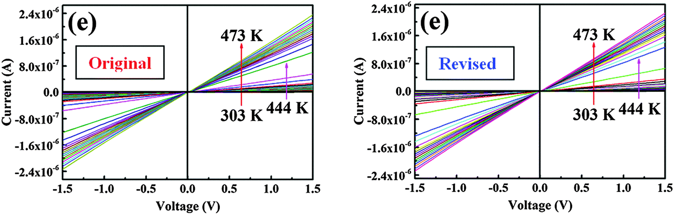

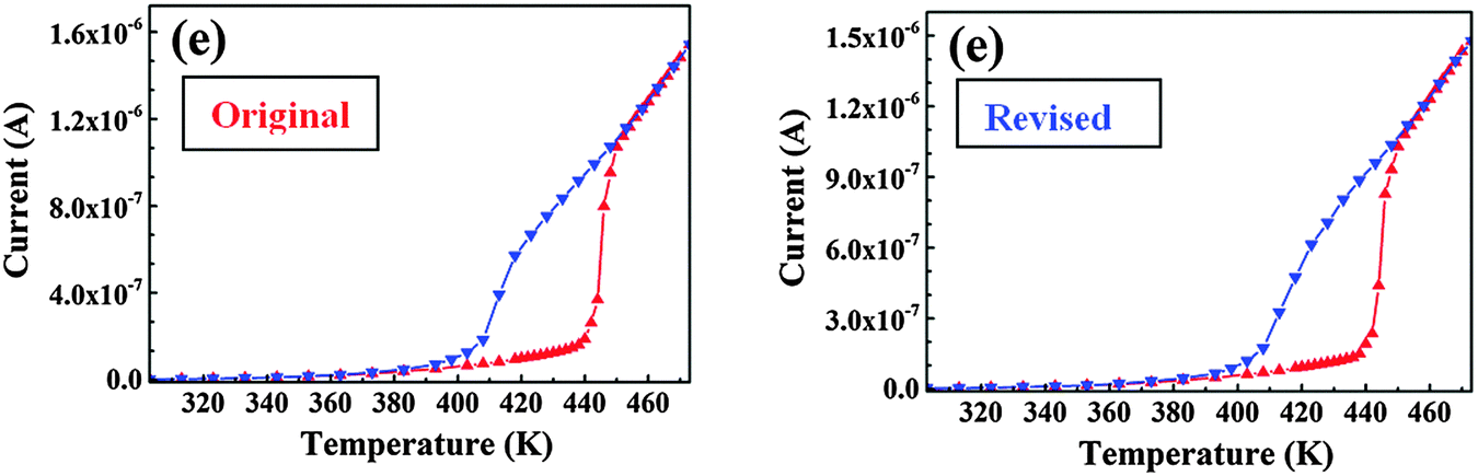
In addition, the green curves in Fig. 6 have been corrected and can be found below.

These changes do not affect any conclusions, because the phase transition temperature, conductivity switching properties and change of resistance during phase transition of 740 nm wide nanowire is very similar with the data of 710 nm wide nanowire used in the original paper.
The Royal Society of Chemistry apologises for these errors and any consequent inconvenience to authors and readers.
| This journal is © the Owner Societies 2016 |