
 Open Access Article
 This Open Access Article is licensed under a
 Creative Commons Attribution 3.0 Unported Licence
Tuning the thermoelectric properties of A-site deficient SrTiO3 ceramics by vacancies and carrier concentration
Deepanshu
Srivastava
a,
Colin
Norman
a,
Feridoon
Azough
a,
Marion C.
Schäfer
b,
Emmanuel
Guilmeau
b,
Demie
Kepaptsoglou
c,
Quentin M.
Ramasse
c,
Giuseppe
Nicotra
d and
Robert
Freer
*a
aSchool of Materials, University of Manchester, Manchester M13 9PL, UK. E-mail: Robert.Freer@manchester.ac.uk
bLaboratoire CRISMAT, 14050 Caen Cedex, France
cSuperSTEM Laboratory, SciTech Daresbury Campus, Daresbury WA4 4AD, UK
dCNR-IMM, Strada VIII, 5, 95121 Catania, Italy
First published on 7th September 2016
Abstract
Ceramics based on Sr0.8La0.067Ti0.8Nb0.2O3−δ have been prepared by the mixed oxide route. The La1/3NbO3 component generates ∼13.4% A-site vacancies; this was fixed for all samples. Powders were sintered under air and reducing conditions at 1450 to 1700 K; products were of high density (>90% theoretical). Processing under reducing conditions led to the formation of a Ti1−xNbxO2−y second phase, core–shell structures and oxygen deficiency. X-ray diffraction (XRD) confirmed a simple cubic structure with space group Pm![[3 with combining macron]](https://www.rsc.org/images/entities/char_0033_0304.gif) m. Transmission electron microscopy revealed a high density of dislocations while analytical scanning transmission electron microscopy at atomic resolution demonstrated a uniform distribution of La, Nb and vacancies in the lattice. X-ray photoemission spectroscopy and thermogravimetry showed the oxygen deficiency (δ value) to be ∼0.08 in reduced samples with enhanced carrier concentrations ∼2 × 1021 cm−3. Both carrier concentration and carrier mobility increased with sintering time, giving a maximum figure of merit (ZT) of 0.25. Selective additional doping by La or Nb, with no additional A site vacancies, led to the creation of additional carriers and reduced electrical resistivity. Together these led to enhanced ZT values of 0.345 at 1000 K. The contributions from oxygen vacancies and charge carriers have been investigated independently.
m. Transmission electron microscopy revealed a high density of dislocations while analytical scanning transmission electron microscopy at atomic resolution demonstrated a uniform distribution of La, Nb and vacancies in the lattice. X-ray photoemission spectroscopy and thermogravimetry showed the oxygen deficiency (δ value) to be ∼0.08 in reduced samples with enhanced carrier concentrations ∼2 × 1021 cm−3. Both carrier concentration and carrier mobility increased with sintering time, giving a maximum figure of merit (ZT) of 0.25. Selective additional doping by La or Nb, with no additional A site vacancies, led to the creation of additional carriers and reduced electrical resistivity. Together these led to enhanced ZT values of 0.345 at 1000 K. The contributions from oxygen vacancies and charge carriers have been investigated independently.
Introduction
Thermoelectricity is the basis for a number of efficient techniques to recover energy from waste heat; applications range from radioisotope thermoelectric generators (RTG) for space missions, to waste heat recovery modules for automotive and industrial environments, and sensors.1 Candidate materials are screened on the basis of the dimensionless figure of merit ZT (defined as S2T/ρκ, where S is the Seebeck coefficient, ρ is the electrical resistivity, κ is the thermal conductivity and T is the temperature).2 Traditional thermoelectric materials such as PbTe have been exploited for over 50 years but tend to degrade at high temperatures. In the past two decades there has been growing interest in oxide thermoelectric materials because of their high chemical and thermal stability, and the relative abundance of their constituent species.3 However, most oxides are intrinsically ionic in nature due to the strong electronegativity of oxygen, which decreases carrier mobility due to charge localization. Nevertheless, the latter may ultimately improve the Seebeck coefficient.4 The interaction of charge carriers with the ionic nature of oxide materials and lattice vibrations results in formation of strongly interacting quasi-particles called polarons. These polarons can influence the overall effective mass of the charge carriers in the system by impeding the flow of carriers, which can subsequently enhance the Seebeck coefficient and the process may be further facilitated by creation of oxygen vacancies and nanostructuring as demonstrated in titanates.5,6Instances of high power factor (PF, defined as S2σ) were initially recorded in layer-structured materials such as the p-type NaxCoO2,7 and this prompted an investigation of other oxides.3,8–10 Amongst the perovskite oxides CaMnO3 was one of the first n-type materials investigated in this context, but only a few studies have reported ZT values higher than 0.15.3,11–13
SrTiO3 (STO) has now emerged as a leading high temperature n-type oxide thermoelectric.14 Undoped SrTiO3 has a high Seebeck coefficient ∼850 μV K−1, a simple cubic structure,15 and is relatively easy to dope with aliovalent cations.16 Lanthanum doping on the A site of SrTiO3 can yield a power factor as high as that of conventional Bi2Te3.17,18 Niobium doping on the B site has raised the high temperature ZT of SrTiO3 to values around 0.35,19,20 due to increases in carrier concentration14 and effective carrier mass.21 A number of authors have reported enhanced thermoelectric properties for oxygen-deficient samples.22,23 However, one of the factors limiting the improvement and practical applicability of SrTiO3-based materials is its high thermal conductivity and its strong temperature dependence,8 frequently limiting ZT to values <0.2. Thermal transport in SrTiO3 is directly correlated with vacancy concentrations and κ can be substantially lowered by cation substitution and disordered site occupancies.6,24,25 Neagu and Irvine26 proposed a mechanism of A-site deficiency to introduce oxygen defects and facilitate further reduction in lattice thermal conductivity (κl).
As a result, strontium titanate has been extensively studied in terms of the effects of different additives and processing conditions. Park et al.27 achieved ZT values above 0.30 at high temperature for La-doped SrTiO3 using colloidal synthesis and spark plasma sintering (SPS), whilst Liu et al.28 and Kovalevsky et al.29 obtained more modest values with Dy doping. Simultaneous doping by La and Nb and optimizing the reducing atmosphere yielded ZT values ∼0.2 at moderate temperatures.30,31 Dehkordi et al.32,33 reported a large improvement in performance with Pr doping of SrTiO3−δ (ZT ∼ 0.35) due to the formation of Pr rich grain boundaries and increased carrier mobility. Related investigations of A-site doping employing Pr, Y and Gd were equally successful for power factor and ZT values.29,34,35 Using pulsed laser deposition, Abutaha et al.36 fabricated superlattice structures comprising 20 pairs of Pr-doped SrTiO3−δ (SPTO) and Nb-doped SrTiO3−δ (STNO) layers, and obtained a very high ZT of 0.46 at 1000 K, improving on the earlier work of Ohta et al.15 who had previously shown that a superlattice based on SrTiO3:SrTi0.8Nb0.2O3 yielded a ZT of 0.24 at 300 K.
Furthermore, rather than focusing on doping or processing parameters alone, many recent investigations of SrTiO3 have employed multiple strategies to improve properties. Kovalevsky et al.29,37–39 demonstrated the effect of defect engineering and co-substitutional doping with lanthanide ions (including Dy). Use of highly-reducing sintering conditions generated Ti3+, oxygen vacancies, A-site vacancies and crystallographic shear structures; together these enabled ZT values up to 0.42.29,40 There is evidence to suggest that an excess number of SrO layers in the SrTiO3 structure decreases overall ZT41 as resistivity increases faster than the reduction in thermal conductivity. However, the work of Liu et al.42 and Shoji et al.43 indicates that a small excess of TiO2 or TiN in the SrTiO3 matrix, can reduce both thermal conductivity and electrical resistivity. Backhaus-Ricoult et al.40 also showed the benefits of having inclusions, oxygen vacancies and shear structures within SrTiO3 matrix.
In this investigation we build on our earlier work on La–Nb doped SrTiO344 and simultaneously dope STO with lanthanum and niobium, by the incorporation during synthesis of 20 mole% of the A-site deficient perovskite La1/3NbO3. This defines the baseline composition such that approximately 13.34% A site vacancies are created in the final material. The addition of excess La and Nb was utilised to generate additional charge carriers without changing the number of cation vacancies. The aim is therefore to separate the contributions from (i) vacancies and (ii) excess charge carriers in enhancing thermoelectric properties.
Experimental methods
The starting powders were: SrCO3 (Sigma Aldrich, UK); La2O3 (Molycorp Inc, USA); TiO2 (Sachtleben Chemie GmbH); Nb2O5 (Solvay, UK); all had >99.9% purity. Prior to use, the La2O3 was heated at 1173 K for 10 h. The powders were mixed in appropriate molar ratios to produce the 0.8(SrTiO3)–0.2(La1/3NbO3)-based samples listed in Table 1.| Sr0.8La0.067Ti0.8Nb0.2O3 | L2 | Base composition |
|---|---|---|
| Sr0.75La0.11Ti0.8Nb0.2O3 | L2-5La | L2 with 5% Sr substituted by La on A-site |
| Sr0.7La0.16Ti0.8Nb0.2O3 | L2-10La | L2 with 10% Sr substituted by La on A-site |
| Sr0.8La0.067Ti0.75Nb0.25O3 | L2-5Nb | L2 with 5% Ti substituted by Nb on B-site |
| Sr0.8La0.067Ti0.7Nb0.3O3 | L2-10Nb | L2 with 10% Ti substituted by Nb on B-site |
For each batch of powder, 0.5 mol% excess TiO2 was added (as a sintering aid), along with equal weights of propan-2-ol and yttria-stabilized zirconia milling balls; batches were vibration milled for 24 h. The resulting slurries were dried, calcined in air at 1373 K, and milled again for 24 h. The final dried powders were passed through a 200 mesh sieve (74 μm) and uniaxially pressed at 90 MPa in a 20 mm diameter hardened steel die to produce cylindrical pellets 5 mm thick. The pellets were placed on 1.5 mm zirconia balls in an alumina crucible and sintered directly in reducing conditions (Ar–5%H2) in a tube furnace (Vecstar model XF6) at 1450–1750 K for times of 8–48 h, with heating/cooling rate of 180 K h−1.
The densities of the sintered ceramics were determined using the Archimedes method. For phase and microstructural analysis, cross-sections of individual specimens were cut using a diamond wheel, then ground and polished down to 1 μm diamond paste prior to use of a silica suspension (OPS). X-ray diffraction (XRD) was carried out using a Philips X'pert diffractometer with a Cu source. The samples were scanned from 10 degrees to 85 degrees 2θ with a step of size 0.020 degrees and dwell time of 10 s at each step. The XRD spectra were refined using the Rietveld program ‘Topas’.45 Scanning electron microscopy (SEM) was undertaken on a Phillips XL30 FEGSEM, equipped with a Rontec X-ray energy dispersive spectroscopy (EDS) system. Average grain sizes were determined using the linear intercept method.46
X-ray photoelectron spectroscopy (XPS) was carried out using a Kratos Axis Ultra instrument with a monochromated Al Kα X-ray source. Samples were polished cross-sections. Detailed scans of electronic transitions of core levels were performed with a resolution of 0.05 eV; data were collected for areas of 700 × 300 μm. Charge compensation was performed for all samples and peak fitting was carried out using CASAXPS software. The carbon 1s peak at 284.8 eV was used for calibration purposes. Background subtraction from acquired data was carried out using the Shirley approximation. All the characteristic peaks were fitted using the GL30 peak shape, which is a mixture of Gaussian plus 30% Lorentzian.
For thermogravimetric analysis, powdered samples were heated in air up to 1700 K in a Netzsch STA 449 C with heating and cooling rates of 2 K min−1. The sintering behaviour of a pressed pellet of L2 formulation (diameter 10 mm, length 5 mm) was investigated up to 1750 K in air using a dilatometer (Netzsch Model 402 C).
The electrical resistivity (ρ) and Seebeck coefficient (S) of the bulk samples were determined from 300 K to 1050 K using a ZEM-III (Ulvac-Riko). Samples were typically 10 mm × 3 mm × 3 mm in size. Charge carrier concentrations were determined by use of a Physical Property Measurement System (Quantum Design-PPMS) at 400 K. The specimens were typically 2.5 mm × 2.5 mm × 0.3 mm in size.
Thermal diffusivity was determined from 300 K to 1100 K using an in-house laser flash facility.47 The Cowan method48 was used to obtain temperature-dependant thermal diffusivity values for all samples. Specific heat capacity was determined by differential scanning calorimetry up to 1000 K (Netzsch STA 449 C).49 The thermal conductivity (κ) was determined as the product of the physical density, the thermal diffusivity and the heat capacity. The overall figure of merit, ZT was determined from the relationship ZT = S2T/ρκ. All properties (ρ, S, κ) were determined on the same bulk specimen.
Samples for TEM and STEM investigations were prepared by a conventional crushing technique; sintered disks were crushed into a powder using an agate mortar and pestle. Grains of individual powders were dispersed in chloroform, dropped onto a copper grid covered with a lacey carbon film, and then dried. Structures were initially investigated using selected area electron diffraction (SAED) and high-resolution transmission electron microscopy (HRTEM) techniques using an FEI FEGTEM (Tecnai G2) operating at 300 kV.
Atomic-resolution structural characterization was carried out using a Nion UltraSTEM100 aberration-corrected dedicated STEM, equipped with a Gatan Enfina Spectrometer. The microscope was operated at 100 kV acceleration voltage and the probe-forming optics were configured to form a ∼0.9 Å probe (full-width at half-maximum) with a convergence semi-angle of 30 mrad and a probe current of 50 pA. The semi-angular ranges of high angle annular dark field and medium angle annular dark field and annular bright field detectors were 86–190, 40–86 and 15–30 mrad, respectively. The native energy spread of the electron probe was 0.35 eV and the collection semi-angle for the electron energy loss spectroscopy measurements was 36 mrad. Additional atomic-resolution characterization was carried out using a JEOL ARM200F probe corrected (S)TEM instrument, equipped with a Gatan Quantum spectrometer and a JEOL Centurio EDX spectrometer. The microscope was operated at 200 kV acceleration voltage and the probe-forming optics were configured to form a ∼0.8 Å probe (full-width at half-maximum). The semi-angular ranges of high angle annular dark field and annular bright field detectors were 72–290 mrad and 18.7–37.8 mrad, respectively. The native energy spread of the electron probe was 0.35 eV and the collection semi-angle for the Electron Energy Loss spectroscopy (EELS) measurements was 100 mrad.
Scanning distortions in the images were corrected using the Jitterbug50 plugin for Digital Micrograph (commercially available from HREM Research Inc.). Image simulations were performed using the QSTEM software package, using parameters matching the experimental conditions.51 Noise in EEL and EDX spectra was removed by Principle Component Analysis using the Cime− EPFL plugin52 for Digital Micrograph.
Results and discussion
Microstructure and phase development
Sintering trials of the L2 base material under reducing conditions (Ar–5%H2) showed the optimum temperature to be 1700 K. Detailed studies were carried out at 1700 K for times of 8 h to 48 h. While samples of L2 sintered in air44 were light grey in colour, the samples sintered in Ar–H2 (this investigation) were black, indicating the presence of Ti3+ or oxygen deficiency.53 All sintered samples were of high density (in excess of 90% theoretical), with density increasing with sintering time (Table 2).| Sintering conditions | Lattice parameter (Å ± 0.001) | Rutile structured phase (±0.1 wt%) | Density (±0.025 g cm−3) | Relative density (±0.5%) |
|---|---|---|---|---|
| Air-8 hour | 3.913 | 0.2 | 4.850 | 94.4 |
| Ar–H2-8 hour | 3.919 | 2.6 | 4.693 | 91.3 |
| Ar–H2-24 hour | 3.923 | 3.3 | 4.915 | 95.5 |
| Ar–H2-48 hour | 3.924 | 4.3 | 5.033 | 97.2 |
An XRD spectrum of an L2 sample sintered for 24 h is shown in Fig. 1. Topas refinement of all XRD spectra confirmed the cubic Pmm space group for all samples. There were also minor amounts of a rutile (TiO2)-type secondary phase, which increased gradually with sintering time (Table 2). Whilst samples sintered in air contained only the equivalent of the excess TiO2 added as a sintering aid (0.2 wt%), those processed under reducing conditions contained significantly more, up to 4.3 wt%.
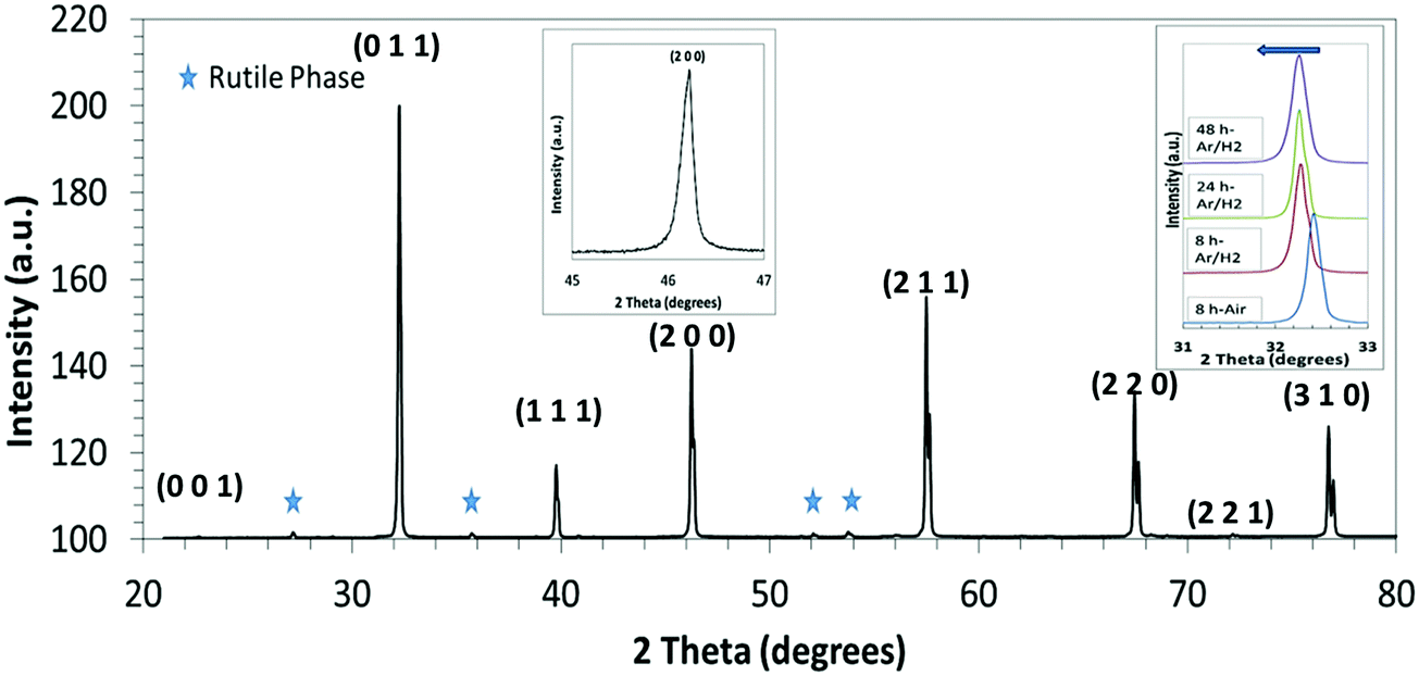 | ||
| Fig. 1 XRD spectrum of the L2 sample sintered in Ar–H2 for 24 h; inset (1) shows details of the (200) peak; inset (2) shows the lateral movement in the (011) peaks for samples sintered for different times. The peaks marked with a star represent a rutile-structured secondary phase. | ||
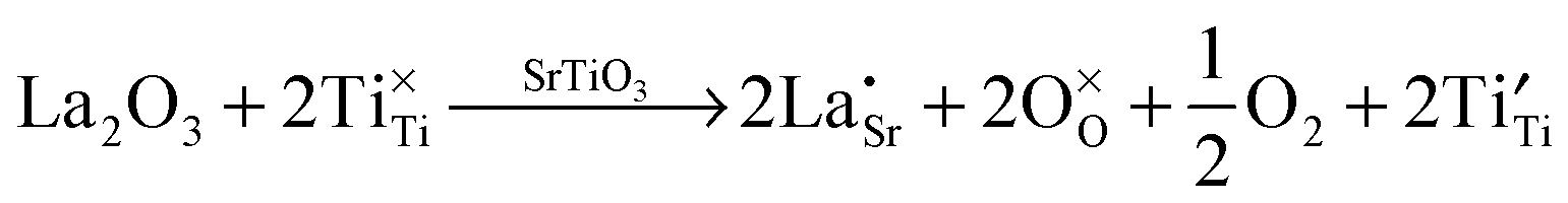
Oxygen vacancies were created in the stoichiometric composition L2 by reduction in the sintering atmosphere as shown in the Kroger–Vink equations below.54 The creation of oxygen vacancies generates free electrons in the system to maintain charge neutrality while O2 gas reacts with H2 to form steam:
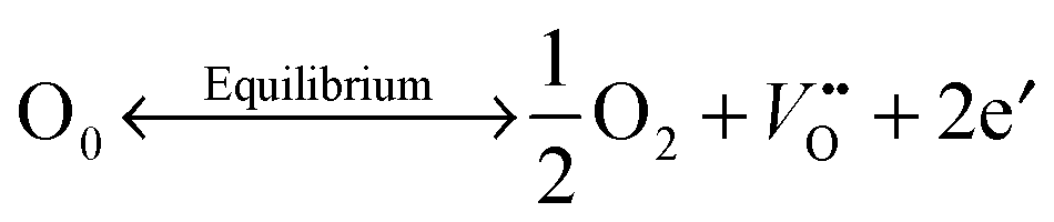 | (1) |
 | (2) |
The evolution of the microstructure is presented in Fig. 2. All L2 specimens exhibit regular polygonal grains, with size increasing with sintering time under reducing conditions; from 7 μm for a time of 8 h (Fig. 2b) to 10 μm for 24 h (Fig. 2c), to 12 μm for 48 h. In contrast, samples sintered for only 8 h in air achieved grain sizes of typically 13 μm (Fig. 2a). Higher magnification, backscattered images of L2 samples sintered in Ar–5%H2 for 24 hours revealed the presence of core–shell structures (Fig. 2d); EDS analysis and mapping indicated that the cores are rich in La and Nb. Detailed analysis indicated that the atomic ratio of Nb![[thin space (1/6-em)]](https://www.rsc.org/images/entities/char_2009.gif) :Ti in the core regions is ∼1:2.8 compared to the stoichiometric ratio of 1:4 in shell regions. The La:Sr ratio was found to be as high as 1:3.5 in the core regions but up to ∼1:12 in the shell regions. The La:Sr/Nb:Ti ratios changed with sintering time under reducing conditions; the core regions were richer in La/Nb in the 24 h samples than in the 48 h samples. These core–shell structures were present in all samples sintered in reducing conditions. When samples were sintered in air for periods up to 24 h, there was very little evidence of La/Nb-rich cores. This suggests that the cores may be the result of an intermediary phase from the calcination process, which is stable in samples sintered in reducing conditions. No additional phases were identified in the calcined powders.
:Ti in the core regions is ∼1:2.8 compared to the stoichiometric ratio of 1:4 in shell regions. The La:Sr ratio was found to be as high as 1:3.5 in the core regions but up to ∼1:12 in the shell regions. The La:Sr/Nb:Ti ratios changed with sintering time under reducing conditions; the core regions were richer in La/Nb in the 24 h samples than in the 48 h samples. These core–shell structures were present in all samples sintered in reducing conditions. When samples were sintered in air for periods up to 24 h, there was very little evidence of La/Nb-rich cores. This suggests that the cores may be the result of an intermediary phase from the calcination process, which is stable in samples sintered in reducing conditions. No additional phases were identified in the calcined powders.
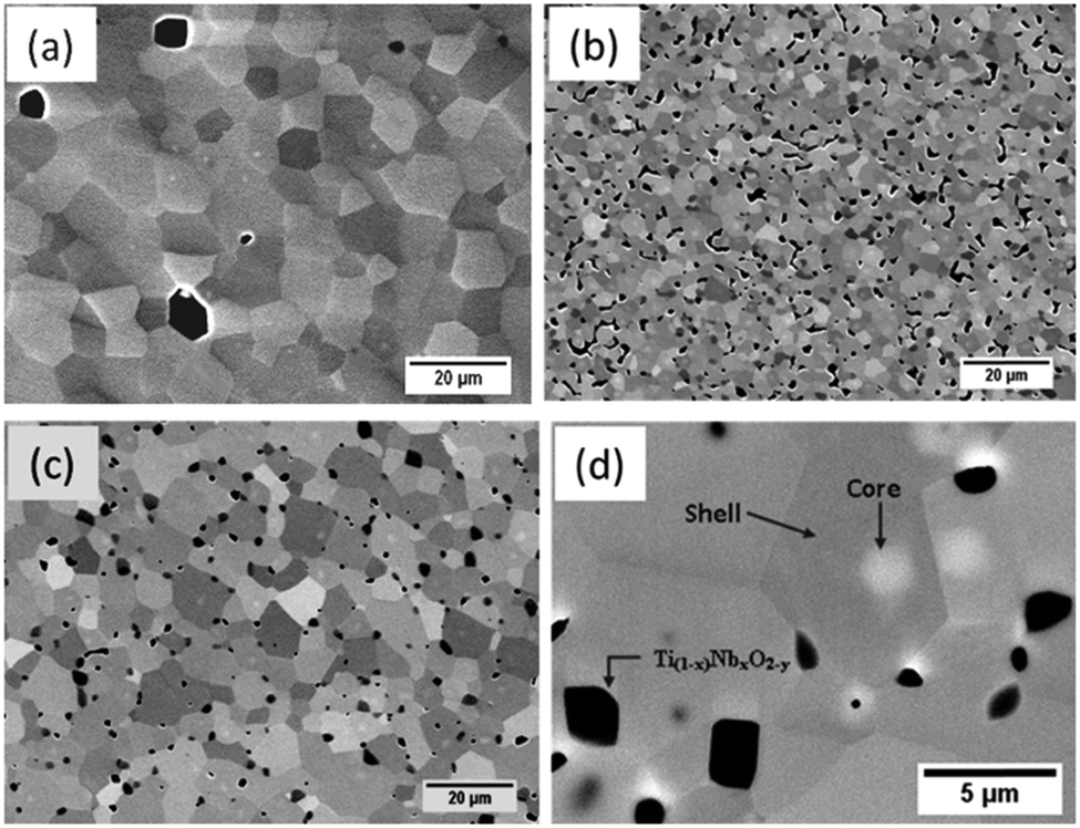 | ||
| Fig. 2 Secondary electron images of L2 samples: (a) sintered in air for 8 h, (b) sintered in Ar–5%H2 for 8 h, and (c) sintered in Ar–5%H2 for 24 h. (d) backscattered image of the L2 sample sintered in Ar–5%H2 for 24 hours. | ||
Another significant feature in the microstructures of samples sintered under reducing conditions was a TiO2-based secondary phase. This was first identified in XRD spectra (Fig. 1) and is visible in SEM micrographs as rectangular to rounded black regions typically 1–2 μm in size (Fig. 2d). The total amount and size of individual regions increased with sintering time. Detailed EDS analysis indicated that these regions are Ti–Nb rich oxides; in samples sintered for 48 hours the Ti:Nb ratio was 10:3. It is proposed that as increasing concentrations of oxygen vacancies are created in the matrix, these Ti(1−x)NbxO2−y based secondary phases are precipitated, mainly at grain boundaries.
Electron microscopy
On a representative example of the samples sintered under reducing conditions, detailed electron microscopy was undertaken on L2 ceramics sintered in Ar–5%H2 for 24 hours. For convenience these samples will be referred to as L2ArH-24h for the remainder of this discussion. A conventional bright field TEM image for L2ArH-24h is shown in Fig. 3a. A high density of dislocations is visible. The presence of dislocations is common in air-sintered, un-doped SrTiO3 ceramics.57,58 However, we are not aware of any reports documenting the presence of dislocations in Ln (La, Nd, Pr) doped or Nb-doped SrTiO3 based ceramics exhibiting good thermoelectric properties and high ZT values.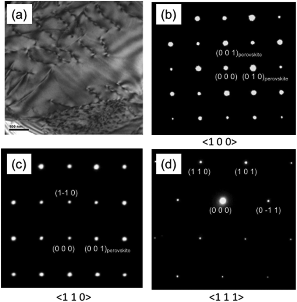 | ||
| Fig. 3 (a) TEM image for the L2-Ar/H2-24h sample. Selected area electron diffraction patterns for major zone axes for the L2-Ar/H2-24h sample along the (b) 〈100〉 (c) 〈110〉 and (d) 〈111〉 zone axes. | ||
To confirm the simple cubic structure deduced from XRD investigation, electron diffraction patterns from three major zone axes were collected (Fig. 3b–d). The diffraction patterns can be indexed as simple cubic symmetry. No extra or diffuse reflections that would suggest the presence of oxygen octahedral tilting, long range or short range ordering can be seen in the diffraction patterns.
To provide further insight into the nature of the reduced Sr0.8La0.067Ti0.8Nb0.2O3 ceramics, an investigation of the atomic structure and chemistry of L2ArH-24h was performed using atomically resolved STEM imaging and EELS measurements.
Fig. 4 shows HAADF STEM images (averaged through rigid registration of a stack of 30 consecutive frames acquired in quick succession) of the L2ArH-24h sample acquired along the [100] and [110] zone axes, respectively. The intensity of A and B sites, observed in the chemically-sensitive Z contrast HAADF images,59 is relatively uniform suggesting a random cation and vacancy distribution throughout the sample. Small site-to-site intensity variations, while present, do not appear to possess any short- to medium-range order, as also evidenced by the absence of additional reflections in the Fourier transform of these images (insets in Fig. 4a and b). Furthermore, no phase separation, defects or other structural domains were observed in the images. As HAADF images are mostly sensitive to heavier elements, often making O columns impossible to distinguish, we have performed Annular Bright Field (ABF) imaging, an imaging mode sensitive to both light and heavy columns allowing for direct imaging of the oxygen positions in the lattice;60 in this imaging mode the atomic positions appear dark on a white background. A representative ABF image (averaged by rigid-registration of 30 consecutive frames acquired in fast succession) acquired along the [110] zone axis of the L2ArH-24h sample is shown in Fig. 4c. In this orientation the B-site (Nb,Ti) columns are separated from both the A-site cations as well as the O columns (see the ball and stick inset in Fig. 4c), which allows for a direct observation of the BO6 octahedral units, and the detection of possible octahedral tilts or distortions of the O sub-lattice. An image simulation using a structural model with Pmm symmetry is overlaid on the image bottom-right corner, showing a good qualitative agreement (in particular for the O column positions). Furthermore, as for the HAADF images, the Fourier transform of the ABF image (inset Fig. 4c) does not reveal any superlattice or long range order reflections. These atomic-scale results thus confirm the findings from XRD and SAED (Fig. 4) that the structure adopts a Pmm symmetry.
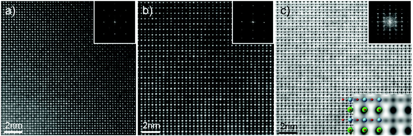 | ||
| Fig. 4 HAADF STEM images and corresponding Fourier transforms (insets) of the L2ArH-24h sample acquired along the [100] (a) and [110] (b) zone axes, respectively. In (a) the atomic columns in the diagonal directions represent the lattice directions of the cubic structure. (c) Annular Bright Field STEM image of the same sample acquired along the [110] axis. The inset in the bottom-right corner corresponds to a simulated ABF image using the Pmm crystal structure, with overlaid ball and stick model of the Pmm structure, where the colour assignment is as follows: A-site, green; B-site; blue and O-site, red. | ||
In order to confirm the absence of any chemical ordering in the sample we employed atomically-resolved chemical mapping through simultaneous EDX and EEL spectrum imaging. Chemical maps were acquired by rastering the electron probe serially across a defined region and simultaneously collecting EELS and EDX spectra at each point. EDX elemental maps were created by integrating, at each point of the spectrum images, the peak intensity of the Sr L, La O, Nb L and Ti K characteristic X-ray peaks. Similarly, EELS elemental maps were created by integrating at each point of the corresponding spectrum images the spectrum intensity over a ∼40 eV window above the Ti L2,3, and La M4,5 EELS edge onsets after background subtraction using a power law model. Fig. 5 shows representative data collected along the [100] direction for the L2ArH-24h sample; the data indicates that both A-site dopants (La and vacancies) and the B-site dopant (Nb) are uniformly distributed throughout the lattice. There is no evidence of any form of cation or vacancy ordering within the field-of-view studied here; additional datasets were acquired throughout the sample with the same conclusions.
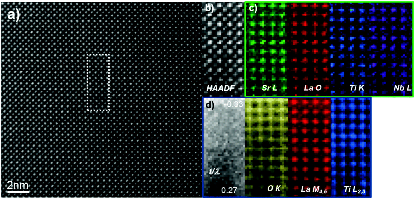 | ||
| Fig. 5 (a) HAADF STEM image of the L2ArH-24h sample, acquired along the [100] zone axis, showing the area used for analysis. (b) HAADF signal acquired simultaneously with (c) EDXS and (d) EELS data. The resulting chemical maps show a highly-uniform distribution of the constituent elements in the lattice. A relative thickness map in (d) (t/λ), (where λ is the inelastic mean free path of the electrons within the material) was also computed, in order to eliminate any possible misinterpretation due to thickness variations within the field of view. | ||
Oxygen deficiency and cation valence state
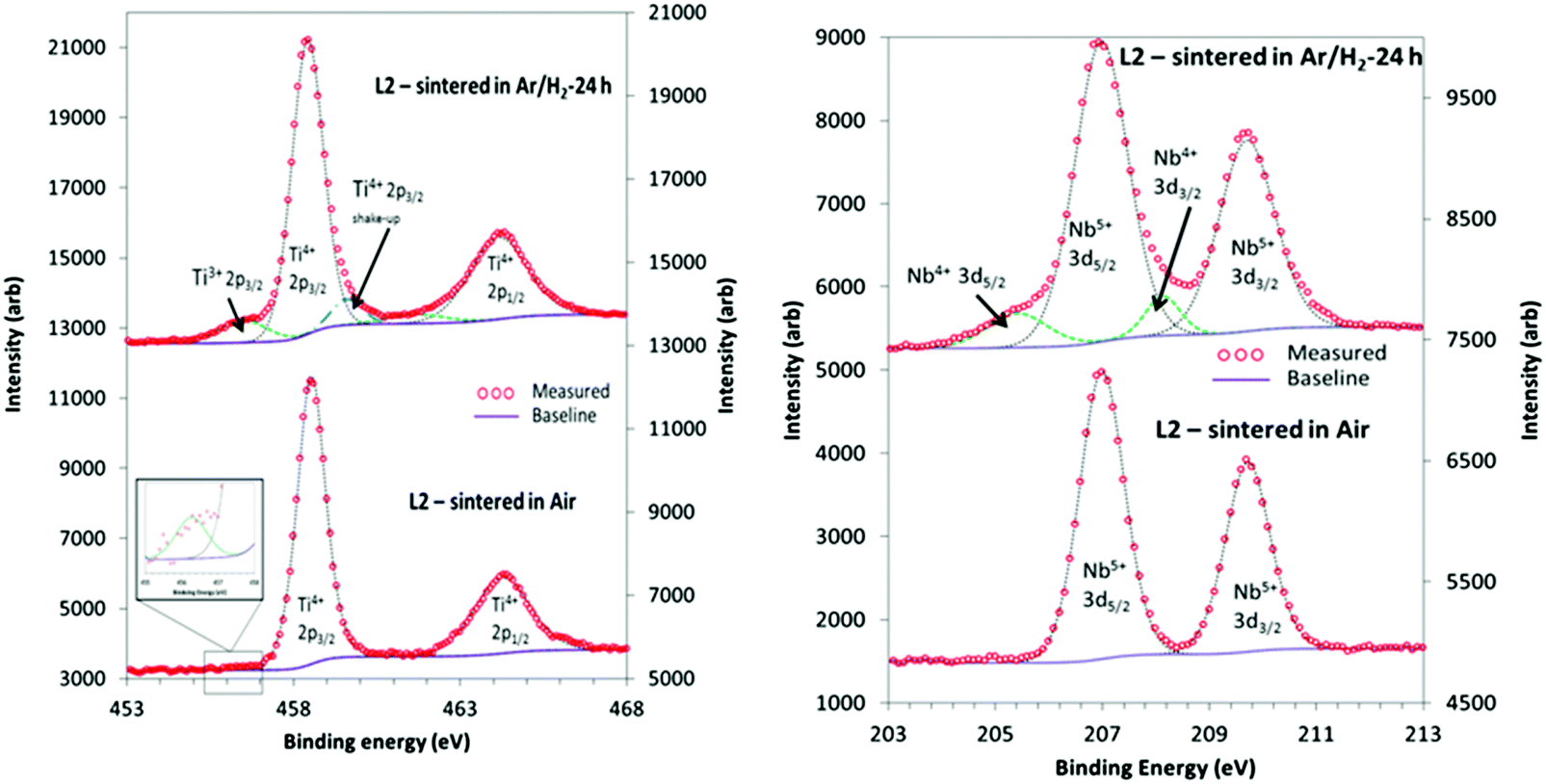 | ||
| Fig. 6 XPS Characteristic doublet peaks obtained for Ti 2p (left) and Nb 3d (right) for L2 samples sintered in air for 8 hours and reducing conditions for 24 hours. | ||
| Sample | L2 Air | L2ArH-8h | L2ArH-24h | L2ArH-48h |
|---|---|---|---|---|
| %Ti3+/total Ti | 1.6 (1) | 8.6 (4) | 10.2 (5) | 11.5 (5) |
| %Nb4+/total Nb | 0 | 11.0 (5) | 10.4 (5) | 10.8 (5) |
Similarly, the XPS data for the L2 samples could be deconvoluted to yield peaks for oxidation states of 4+ and 5+ for Nb 3d. Fig. 6b shows the 3d5/2 and 3d3/2 doublet, with peak positions of 206.9 eV and 209.7 eV, and a separation of 2.7 eV. In most of the reduced samples the amount of Nb4+ as a fraction of total Nb was typically 11% (Table 3), whilst there was no Nb4+ in the air-sintered samples. In general, samples sintered in reducing conditions exhibited a higher concentration of Ti3+ than Nb4+ oxidation states, and the fraction of Ti3+ increased with sintering time.
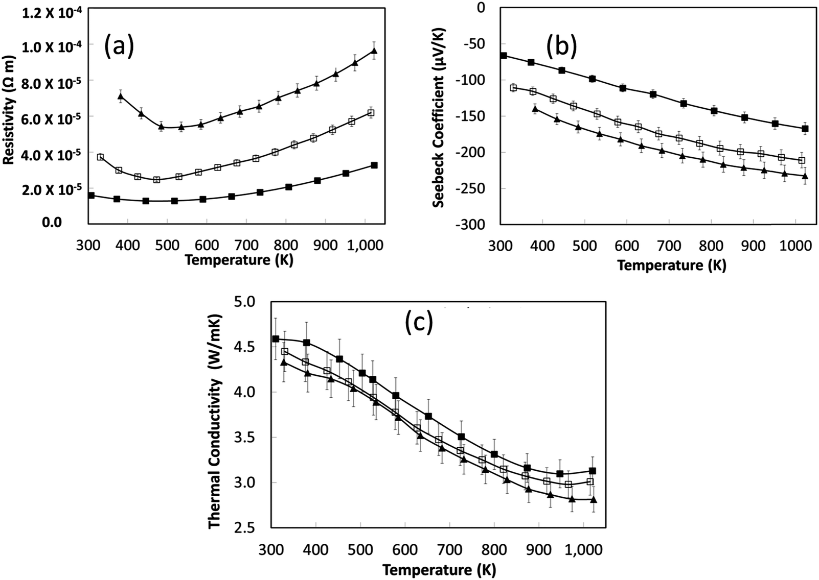 | ||
| Fig. 7 Temperature dependence of (a) the electrical resistivity, (b) the Seebeck coefficient and (c) the total thermal conductivity for L2 samples sintered under reducing conditions. The legend key is as follows: L2-(Ar/H2)-8 hours is represented by closed triangle (▲); L2-(Ar/H2)-24 hours is represented by open square (□); L2-(Ar/H2)-48 hours is represented by closed square (■). | ||
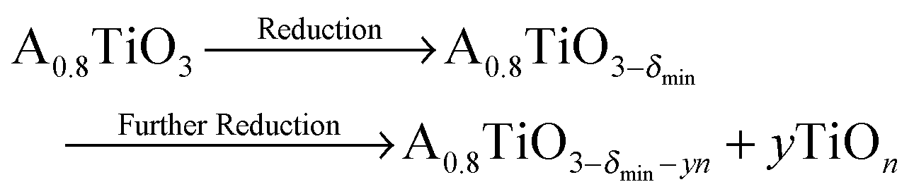
In Fig. 2, the concentration of microstructural defects in L2 sample was observed to change with increase in sintering time. The density of the samples and the quantity of secondary phase segregation of (Ti,Nb)O2−x increased with sintering time (Table 2), while the change in core–shell structure with time was insignificant. This increase in density is related to increase in effective diffusion distance during sintering, which is proportional to the square root of sintering time  .64 On the other hand, the increasing reduction of SrTiO3 based samples in Ar/H2 results in increasing segregation of TiO2−y phase at grain boundaries and triple point junctions. Irvine et al.65 showed that sintering A-site deficient titanates in a reducing atmosphere exsolves TiO2 after an oxygen deficiency limit (δmin) is reached, as shown in eqn (3):
 | (3) |
The baseline L2 samples contain 13.3% A site vacancies,44 which are maintained in oxidised and reduced samples. In addition, the oxygen vacancies, grain boundaries, second phases and distributed core–shell structures will also contribute to phonon scattering and help to improve thermoelectric performance. In general, thermal conductivity was at least 10–12% lower for samples with core–shell structures than for the samples without them. Collectively, the various structural defects can help reduce the lattice thermal conductivityκl.
The grain sizes for the L2 samples sintered in Ar/H2 increased from 7–12 μm with increase in sintering time. This variation should modify the volume of grain boundary interface regions and the scattering centres in the bulk specimen, and possibly affect thermal conductivity. However, the grain sizes for the L2 samples are relatively large (several microns) and the variation modest. Koumoto et al.8 demonstrated that grain size changes only had a significant effect on thermal conductivity when grain sizes were in the range of few tens of nanometres. This is also supported by the fact that the temperature-dependent average phonon mean paths in SrTiO3 based materials of the order of 1–2 nm and not significantly affected by the grain sizes of order of microns.
The total thermal conductivity is the sum of the lattice and electronic thermal conductivity. The electronic thermal conductivity8κe is given by:
| κe = L0Tσ | (4) |
The small increase in total κ with increased sintering time is again associated with an increase in carrier concentration. Nevertheless, the total thermal conductivity of the reduced samples (Fig. 7c) is significantly less than for air-sintered samples, typically 12 W m−1 K−1 at room temperature to 5 W m−1 K−1 at 1000 K.66 Disordering of A-site vacancies remains a dominant factor for the thermal conductivity reduction.
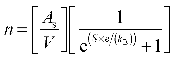
Charge carrier concentrations for the L2 samples were determined experimentally and calculated via the modified Hiekes' equation:67
 | (5) |
 is the number of available sites per unit volume of unit cell; for the cubic peroskite structure As is 1 and the cell constant is ≅0.3905 nm. The quantity ((kB)/e) is the ratio of the Boltzmann constant to the electronic charge and is approximately equal to 87 μV K−1; S is the Seebeck coefficient. The use of Hiekes formula assumes negligible spin orbit degeneracy and configurational entropy contributions to thermopower67 and is used here only to determine the approximate levels of carrier concentration. More detailed understanding of material dependant properties and use of Mott's formula might be more suitable to estimate well correlated values of carrier concentration compared to calculated values obtained by the Hall measurements. The collected data (Table 4) show that carrier concentrations in the L2 samples are approximately 4 × 1021 cm−3 and increased with sintering time and the increasing degree of reduction. In contrast, carrier concentrations in air-sintered samples are typically three orders of magnitude lower.
| Sintering conditions | Carrier concentration (cm−3) (±10%) | Charge mobility (cm2 V−1 s−1) | m*/m0 | m*/n2/3 (10−14 cm2) | |
|---|---|---|---|---|---|
| Calculated | Experimental | ||||
| Air-8 hour | 1.58 × 10¹⁸ | 0.79 | 0.273 | 0.199 m0 | |
| Ar–H2-8 hour | 1.02 × 10²¹ | 0.86 | 3.84 | 3.727 m0 | |
| Ar–H2-24 hour | 4.19 × 10²¹ | 1.69 × 10²¹ | 1.34 | 4.30 | 2.98 m0 |
| Ar–H2-48 hour | 6.67 × 10²¹ | 2.83 × 10²¹ | 1.64 | 4.04 | 1.987 m0 |
To provide further insight into the nature of the samples, charge mobility and effective mass values were calculated. The charge mobility (μ) was obtained via the standard conductivity relationship, eqn (6):
| σ = neμ | (6) |
 as shown by eqn (7):56,68
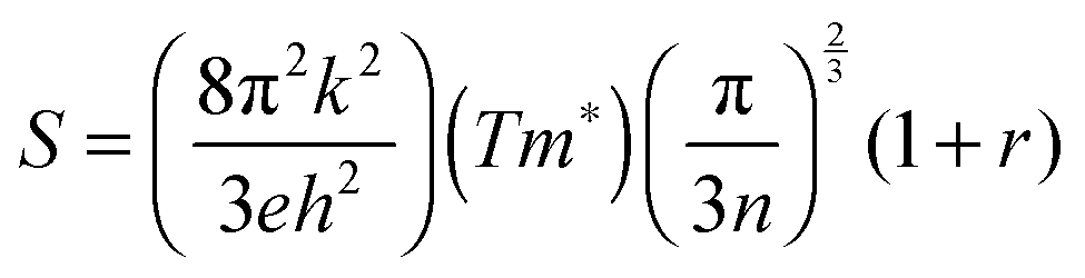 | (7) |
Based on the thermoelectric parameters presented in Fig. 7, the thermoelectric figure of merit (ZT) was determined (Fig. 8). With increasing sintering time under reducing conditions there was a steady increase in ZT to a maximum value of 0.27 at 1000 K; samples sintered for 8 hours had a peak ZT of 0.2. This demonstrates the importance of the reducing environments for processing SrTiO3-based materials; the same materials sintered in air attained a maximum ZT value of 0.004 at 1000 K.44 The improvement in ZT with increased sintering time under reducing conditions can be linked directly to the steady increase in carrier concentration with sintering time (Table 4). However, carrier mobility did not improve by the same degree suggesting strong scattering of carriers within the bulk material.
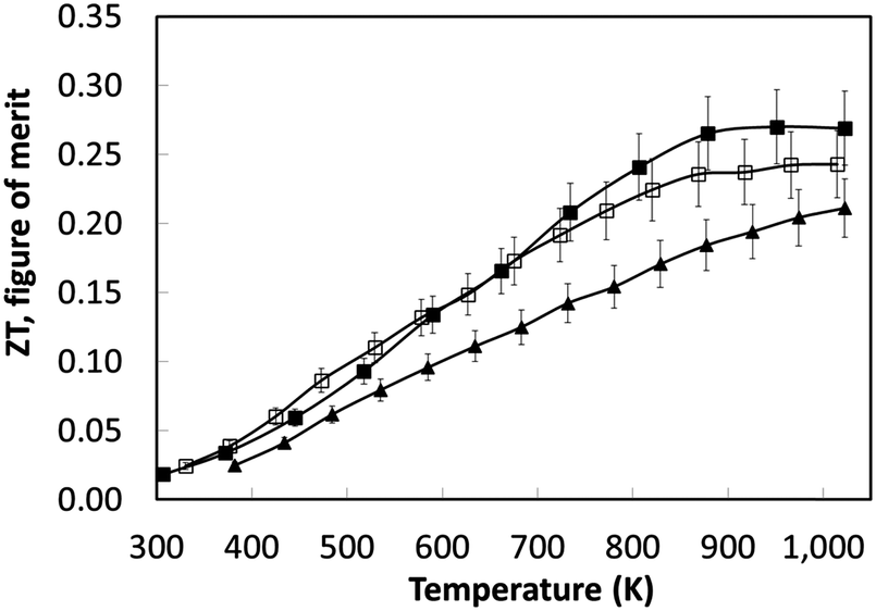 | ||
| Fig. 8 Temperature dependence of the thermoelectric figure of merit for L2 samples sintered under reducing conditions. The legend key is as follows: L2-(Ar/H2)-8 hours is represented by closed triangle (▲); L2-(Ar/H2)-24 hours is represented by open square (□); L2-(Ar/H2)-48 hours is represented by closed square (■). | ||
With the control of the processing environment, the composition, the carrier concentration and the effective TE properties can be optimised and improved significantly. So far we have focussed on the effect of changing δ, and therefore the oxygen vacancy concentration, whilst the A site vacancy concentration was fixed. Having now optimised processing conditions for Sr0.8La0.067Ti0.8Nb0.2O3 we maintain the A-site vacancy concentration, but vary the number of excess charge carriers through doping on the A and B sites, to separately define the contribution of excess carriers.
Lanthanum doping of SrTiO3 on the A site increases the number of charge carriers and generates surplus electrons. The latter are charge-compensated by reduction of Ti from 4+ to 3+. These changes can be represented by the following Kröger–Vink equations, which has been discussed in detail by Koumoto et al.8 These effects are independent of the reduction that occurs during sintering, which also gives rise to additional charge carriers.
 | (8) |
 | (9) |
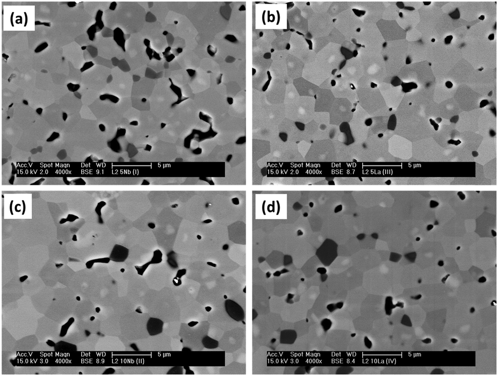 | ||
| Fig. 9 Backscattered SEM images: (a) L2-5Nb; (b) L2-5La; (c) L2-10Nb; (d) L2-10La. | ||
The thermoelectric properties of the samples shown in Fig. 9 are presented in Fig. 10. The electrical resistivities of the excess doped materials were significantly lower than the baseline L2 material (Fig. 10a). The resistivity of L2-5La and L2-10La samples are similar. Whilst La3+ substitution reduces the electrical resistivity compared to the baseline L2 material, there is no systematic trend for additions of La. In contrast, Nb substitution systematically improves electrical conductivity; L2-10Nb has the lowest electrical resistivity of all the samples. The Seebeck coefficients of lanthanum-doped samples were marginally higher than for niobium-doped samples (Fig. 10b); values for all the samples range between −50 μV K−1 at 300 K to −160 μV K−1 at 1000 K.
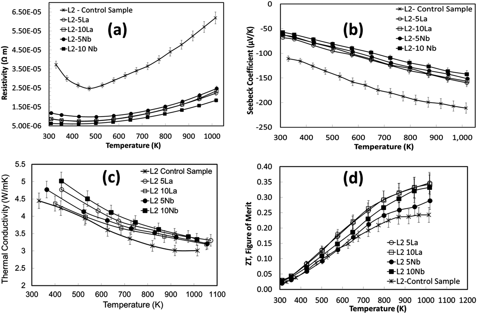 | ||
| Fig. 10 Temperature dependence of thermoelectric properties for doped L2 samples sintered under reducing conditions: (a) resistivity; (b) Seebeck coefficient; (c) thermal conductivity; (d) figure of merit. Key for symbols: × – base L2 composition; ● – L2 5Nb; ■ – L2 10Nb; ○ – L2 5La; □ – L2 10 La. | ||
In the present study, the variation of thermal conductivity with excess doping was not significant, and only marginally different from the control sample. This can be attributed to the constant concentration of vacancies in the doped L2 samples, giving average thermal conductivities of 5 W m−1 K−1 to 3 W m−1 K−1 across the temperature range (Fig. 10c). It should be noted that excess doping of lanthanum and niobium actually increases the total thermal conductivity due to an increase in electronic thermal conductivity.
The temperature dependence of ZT for these samples is presented in Fig. 10d. The use of excess La and Nb has been beneficial; the ZT values for all the doped samples are higher than for the baseline L2 material, which had a maximum ZT value of 0.25. Samples prepared with 10% excess Nb had ZT values of 0.32 at 1000 K, whilst samples prepared with 5% excess La exhibited the highest ZT values of 0.345 at 1000 K. Clearly, the generation of additional charge carriers, through the combination of both reducing sintering conditions and excess doping by La or Nb, is a particularly effective strategy for improving the performance or SrTiO3-based thermoelectric materials. Although the overall figure of merit for La and Nb doped samples are not significantly different, the values for both are significantly higher than for the baseline L2 – 24 hours Ar/5%H2 sample. Indeed, a selective approach can be employed to enhance thermoelectric properties. Firstly, the carrier concentration can be increased, and then independently the charge mobility can be improved by modifying the grain boundary resistance and the effective carrier mass 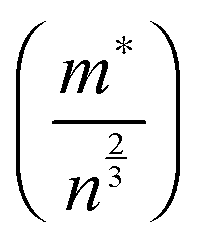 without affecting carrier concentration. One example of the latter approach was highlighted in the work of Wang et al. on yttria-stabilised zirconia nano-inclusions in Nb-doped SrTiO3.23 However, the present work demonstrates unambiguously the relative contributions from the two strategies based on vacancy concentrations and carrier concentrations.
Conclusions
High quality Sr0.8La0.067Ti0.8Nb0.2O3−δ ceramics were prepared under reducing conditions. The presence of 20 mole% La1/3NbO3 in the SrTiO3 base material generates ∼13% vacancies on the A-sites; this fraction was fixed across all compositions. The physical properties, microstructure and thermoelectric properties were highly dependent on the sintering conditions, reflecting changes in defect concentrations and second phase development. Grain sizes were typically 7–10 μm where sintered in reducing conditions, but ∼13 μm when sintered in air. The materials exhibited a simple cubic structure (Pmm space group) which did not change with processing conditions. However, as samples were sintered for increasing time under reducing conditions there were increasing amounts of a Ti1−xNbxO2−y second phase, as well as the formation of core–shell structures. Both helped to reduce thermal conductivity.
TEM investigations confirmed the cubic symmetry and revealed a high density of dislocations and linear imperfections within the grains. STEM-EELS and STEM-EDXS investigations at atomic resolution demonstrated conclusively a uniform distribution of La, Nb and cation vacancies within the lattice, with no evidence of any ordering or superlattice structures. The presence of ∼13% A-site vacancies helps to reduce the electrical resistivity by approximately 50% compared to (undoped) SrTiO3. Processing under reducing conditions led to oxygen deficiencies. XPS and thermogravimetry demonstrated an oxygen deficiency, δ = 0.082 for the samples sintered for 24 hours. The resulting increase in carrier concentration (three orders of magnitude compared to air-sintered samples) and approximate doubling of the carrier mobility significantly improved the power factor, and led to a thermoelectric figure of merit (ZT) of 0.25 at 1000 K.
Further systematic improvement in thermoelectric properties was achieved by selective doping by lanthanum and niobium. By using up to 10% excess La or Nb it was possible to generate additional charge carriers, while maintaining a constant concentration of A-site vacancies. Grain sizes were much smaller (<5 μm) and there was still evidence of the Ti1−xNbxO2−y second phase. The presence of additional charge carriers reduced the electrical resistivity by up to one order of magnitude. In contrast, the additional carriers marginally increased thermal conductivity as the extra La or Nb increased the electronic component of thermal conductivity. As a result, high values of ZT of 0.25 to 0.345 were achieved at 700 to 1000 K. Further improvements should be possible by improving the carrier concentrations and mobility, and by reducing grain boundary resistance while maintaining similar A-site vacancy concentrations. Nevertheless, the present work demonstrates unambiguously the relative contributions from the two strategies based on vacancy concentrations and carrier concentrations.
Acknowledgements
The authors are grateful to the EPSRC for the provision of funding for this work (EP/H043462, EP/I036230/1, EP/L014068/1, EP/L017695/1 acknowledged by RF) and continued funding for the SuperSTEM facility since 2002 (including EP/D040205/1, EP/D040396/1, EP/D040566/1, and the current support as an EPSRC National Facility for Aberration-Corrected Scanning Transmission Electron Microscopy; acknowledged by DMK, QMR). D. S. acknowledges support through the provision of a President's Scholarship from the University of Manchester.References
- T. M. Tritt, Annu. Rev. Mater. Res., 2011, 41, 433–448 CrossRef CAS.
- D. M. Rowe, Thermoelectrics handbook macro to nano, CRC Press, Boca Raton, 2006 Search PubMed.
- J. W. Fergus, J. Eur. Ceram. Soc., 2012, 32, 525–540 CrossRef CAS.
- G. J. Snyder and E. S. Toberer, Nat. Mater., 2008, 7, 105–114 CrossRef CAS PubMed.
- W. S. Choi, H. Ohta, S. J. Moon, Y. S. Lee and T. W. Noh, Phys. Rev. B: Condens. Matter Mater. Phys., 2010, 82, 024301 CrossRef.
- W. S. Choi, H. K. Yoo and H. Ohta, Adv. Funct. Mater., 2015, 25, 799–804 CrossRef CAS.
- I. Terasaki, Y. Sasago and K. Uchinokura, Phys. Rev. B: Condens. Matter Mater. Phys., 1997, 56, 12685–12687 CrossRef.
- K. Koumoto, Y. F. Wang, R. Z. Zhang, A. Kosuga and R. Funahashi, Annu. Rev. Mater. Res., 2010, 40, 363–394 CrossRef CAS.
- G. K. Ren, J. L. Lan, C. C. Zeng, Y. C. Liu, B. Zhan, S. Butt, Y. H. Lin and C. W. Nan, JOM, 2015, 67, 211–221 CrossRef CAS.
- W. S. Liu, Q. Jie, H. S. Kim and Z. F. Ren, Acta Mater., 2015, 87, 357–376 CrossRef CAS.
- L. Bocher, M. H. Aguirre, D. Logvinovich, A. Shkabko, R. Robert, M. Trottmann and A. Weidenkaff, Inorg. Chem., 2008, 47, 8077–8085 CrossRef CAS PubMed.
- M. Molinari, D. A. Tompsett, S. C. Parker, F. Azough and R. Freer, J. Mater. Chem. A, 2014, 2, 14109–14117 CAS.
- D. Srivastava, F. Azough, R. Freer, E. Combe, R. Funahashi, D. M. Kepaptsoglou, Q. M. Ramasse, M. Molinari, S. R. Yeandel, J. D. Barand and S. C. Parker, J. Mater. Chem. C, 2015, 3, 12245–12259 RSC.
- H. Ohta, K. Sugiura and K. Koumoto, Inorg. Chem., 2008, 47, 8429–8436 CrossRef CAS PubMed.
- H. Ohta, S. Kim, Y. Mune, T. Mizoguchi, K. Nomura, S. Ohta, T. Nomura, Y. Nakanishi, Y. Ikuhara, M. Hirano, H. Hosono and K. Koumoto, Nat. Mater., 2007, 6, 129–134 CrossRef CAS PubMed.
- J. Ravichandran, W. Siemons, D. W. Oh, J. T. Kardel, A. Chari, H. Heijmerikx, M. L. Scullin, A. Majumdar, R. Ramesh and D. G. Cahill, Phys. Rev. B: Condens. Matter Mater. Phys., 2010, 82, 165126 CrossRef.
- T. Okuda, K. Nakanishi, S. Miyasaka and Y. Tokura, Phys. Rev. B: Condens. Matter Mater. Phys., 2001, 63, 113104 CrossRef.
- H. Muta, K. Kurosaki and S. Yamanaka, J. Alloys Compd., 2005, 392, 306–309 CrossRef CAS.
- S. Ohta, H. Ohta and K. Koumoto, J. Ceram. Soc. Jpn., 2006, 114, 102–105 CrossRef CAS.
- K. Kato, M. Yamamoto, S. Ohta, H. Muta, K. Kurosaki, S. Yamanaka, H. Iwasaki, H. Ohta and K. Koumoto, J. Appl. Phys., 2007, 102, 116107 CrossRef.
- W. Wunderlich, H. Ohta and K. Koumoto, Phys. B, 2009, 404, 2202–2212 CrossRef CAS.
- J. Liu, C. L. Wang, W. B. Su, H. C. Wang, P. Zheng, J. C. Li, J. L. Zhang and L. M. Mei, Appl. Phys. Lett., 2009, 95, 162110 CrossRef.
- W. H. Gong, H. Yun, Y. B. Ning, J. E. Greedan, W. R. Datars and C. V. Stager, J. Solid State Chem., 1991, 90, 320–330 CrossRef CAS.
- S. R. Popuri, A. J. M. Scott, R. A. Downie, M. A. Hall, E. Suard, R. Decourt, M. Pollet and J. W. G. Bos, RSC Adv., 2014, 4, 33720–33723 RSC.
- Z. L. Lu, H. R. Zhang, W. Lei, D. C. Sinclair and I. M. Reaney, Chem. Mater., 2016, 28, 925–935 CrossRef CAS.
- D. Neagu and J. T. S. Irvine, Chem. Mater., 2011, 23, 1607–1617 CrossRef CAS.
- K. Park, J. S. Son, S. I. Woo, K. Shin, M. W. Oh, S. D. Park and T. Hyeon, J. Mater. Chem. A, 2014, 2, 4217–4224 CAS.
- J. Liu, C. L. Wang, H. Peng, W. B. Su, H. C. Wang, J. C. Li, J. L. Zhang and L. M. Mei, J. Electron. Mater., 2012, 41, 3073–3076 CrossRef.
- A. V. Kovalevsky, A. A. Yaremchenko, S. Populoh, P. Thiel, D. P. Fagg, A. Weidenkaff and J. R. Frade, Phys. Chem. Chem. Phys., 2014, 16, 26946–26954 RSC.
- T. Teranishi, Y. Ishikawa, H. Hayashi, A. Kishimoto, M. Katayama and Y. Inada, J. Am. Ceram. Soc., 2013, 96, 2852–2856 CrossRef CAS.
- H. C. Wang, C. L. Wang, W. B. Su, J. Liu, H. Peng, J. L. Zhang, M. L. Zhao, J. C. Li, N. Yin and L. M. Mei, J. Alloys Compd., 2009, 486, 693–696 CrossRef CAS.
- A. M. Dehkordi, S. Bhattacharya, T. Darroudi, J. W. Graff, U. Schwingenschlogl, H. N. Alshareef and T. M. Tritt, Chem. Mater., 2014, 26, 2478–2485 CrossRef.
- A. M. Dehkordi, S. Bhattacharya, J. He, H. N. Alshareef and T. M. Tritt, Appl. Phys. Lett., 2014, 104, 193902 CrossRef.
- C. Chen, T. S. Zhang, R. Donelson, T. T. Tan and S. Li, J. Alloys Compd., 2015, 629, 49–54 CrossRef CAS.
- H. Muta, K. Kurosaki and S. Yamanaka, J. Alloys Compd., 2003, 350, 292–295 CrossRef CAS.
- A. I. Abutaha, S. R. S. Kumar, K. Li, A. M. Dehkordi, T. M. Tritt and H. N. Ashareef, Chem. Mater., 2015, 27, 2165–2171 CrossRef CAS.
- A. V. Kovalevsky, S. Populoh, S. G. Patricio, P. Thiel, M. C. Ferro, D. P. Fagg, J. R. Frade and A. Weidenkaff, J. Phys. Chem. C, 2015, 119, 4466–4478 CAS.
- A. V. Kovalevsky, A. A. Yaremchenko, S. Populoh, A. Weidenkaff and J. R. Frade, J. Phys. Chem. C, 2014, 118, 4596–4606 CAS.
- A. A. Yaremchenko, S. Populoh, S. G. Patricio, J. Macias, P. Thiel, D. P. Fagg, A. Weidenkaff, J. R. Frade and A. V. Kovalevsky, Chem. Mater., 2015, 27, 4995–5006 CrossRef CAS.
- M. Backhaus-Ricoult, J. R. Rustad, D. Vargheese, I. Dutta and K. Work, J. Electron. Mater., 2012, 41, 1636–1647 CrossRef CAS.
- Y. F. Wang, C. L. Wan, X. Y. Zhang, L. M. Shen, K. Koumoto, A. Gupta and N. Z. Bao, Appl. Phys. Lett., 2013, 102, 183905 CrossRef.
- J. Liu, H. C. Wang, W. B. Su, C. L. Wang, J. L. Zhang and L. M. Mei, Solid State Sci., 2010, 12, 134–137 CrossRef CAS.
- T. Shoji, S. Sugiyama and K. Fuda, Mater. Trans., 2011, 52, 1531–1534 CrossRef CAS.
- D. Srivastava, F. Azough, M. Molinari, S. C. Parker and R. Freer, J. Electron. Mater., 2015, 44, 1803–1808 CrossRef CAS.
- H. M. Rietveld, Acta Crystallogr., 1967, 22, 151–152 CrossRef CAS.
- M. I. Mendelson, J. Am. Ceram. Soc., 1969, 52, 443–448 CrossRef CAS.
- R. Taylor, J. Phys. E: Sci. Instrum., 1980, 13, 1193–1199 CrossRef CAS.
- R. D. Cowan, J. Appl. Phys., 1963, 34, 926–930 CrossRef CAS.
- J. E. Daw, Measurement of specific heat capacity using differential scanning calorimeter, U.S. Department of Energy National Laboratory, Idaho, 2008 Search PubMed.
- L. Jones and P. D. Nellist, Microsc. Microanal., 2013, 19, 1050–1060 CrossRef CAS PubMed.
- C. Koch, PhD thesis, Arizona State University, 2002.
- G. Lucas, P. Burdet, M. Cantoni and C. Hébert, Micron, 2013, 52–53, 49–56 CrossRef CAS PubMed.
- S. A. Prosandeev, I. P. Raevski and M. A. Bunin, Phys. Rev. B: Condens. Matter Mater. Phys., 2004, 70, 157101 CrossRef.
- K. Koumoto, Y. F. Wang, R. Z. Zhang, A. Kosuga and R. Funahashi, Annu. Rev. Mater. Res., 2010, 40, 363–394 CrossRef CAS.
- Z. Lu, H. Zhang, W. Lei, D. C. Sinclair and I. M. Reaney, Chem. Mater., 2016, 28, 925–935 CrossRef CAS.
- M. G. Sahini, J. R. Tolchard, K. Wiik and T. Grande, Dalton Trans., 2015, 44, 10875–10881 RSC.
- T. Matsunaga and H. Saka, Philos. Mag. Lett., 2000, 80, 597–604 CrossRef CAS.
- S. B. Lee, W. Sigle, F. Phillipp and D. Brunner, Acta Mater., 2005, 53, 1843–1848 CrossRef CAS.
- S. J. Pennycook and P. D. Nellist, Scanning transmission electron microscopy: imaging and analysis, Springer Science & Business Media, 2011 Search PubMed.
- S. D. Findlay, N. Shibata, H. Sawada, E. Okunishi, Y. Kondo, T. Yamamoto and Y. Ikuhara, Appl. Phys. Lett., 2009, 95, 191913 CrossRef.
- M. S. J. Marshall, D. T. Newell, D. J. Payne, R. G. Egdell and M. R. Castell, Phys. Rev. B: Condens. Matter Mater. Phys., 2011, 83, 35410 CrossRef.
- NIST, X-ray Photoelectron Spectroscopy Database, Material Measurement Laboratory (MML), Gaithersburg, 2012 Search PubMed.
- P. Blennow, A. Hagen, K. K. Hansen, L. R. Wallenberg and M. Mogensen, Solid State Ionics, 2008, 179, 2047–2058 CrossRef CAS.
- W. D. Kingery, Introduction to ceramics, John Wiley & Sons, 1960 Search PubMed.
- D. Neagu and J. T. S. Irvine, Chem. Mater., 2010, 22, 5042–5053 CrossRef CAS.
- Y. F. Wang, K. Fujinami, R. Z. Zhang, C. L. Wan, N. Wang, Y. S. Ba and K. Koumoto, Appl. Phys. Express, 2010, 3, 31101 CrossRef.
- H. Taguchi, M. Sonoda and M. Nagao, J. Solid State Chem., 1998, 137, 82–86 CrossRef CAS.
- M. Cutler, J. F. Leavy and R. L. Fitzpatrick, Phys. Rev., 1964, 133, 1143–1152 CrossRef CAS.
- S. Ohta, T. Nomura, H. Ohta and K. Koumoto, J. Appl. Phys., 2005, 97, 34106 CrossRef.
| This journal is © the Owner Societies 2016 |