
 Open Access Article
 This Open Access Article is licensed under a
 Creative Commons Attribution 3.0 Unported Licence
Morphological modulation of graphene-mediated hybridization in plasmonic systems†
Niloofar
Haghighian
a,
Francesco
Bisio
*b,
Vaidotas
Miseikis
c,
Gabriele C.
Messina
d,
Francesco
De Angelis
d,
Camilla
Coletti
ce,
Alberto
Morgante
fg and
Maurizio
Canepa
a
aOptMatLab, Dipartimento di Fisica, Università degli Studi di Genova, via Dodecaneso 33, 16146 Genova, Italy
bCNR-SPIN, C.so Perrone 24, 16152 Genova, Italy. E-mail: francesco.bisio@spin.cnr.it; Fax: +39 010314218; Tel: +39 0103536287
cCenter for Nanotechnology Innovation@NEST, Istituto Italiano di Tecnologia, Piazza S. Silvestro 12, 56127 Pisa, Italy
dIstituto Italiano di Tecnologia, Via Morego 30, 16163 Genova, Italy
eGraphene Labs, Istituto Italiano di Tecnologia, Via Morego 30, 16163 Genova, Italy
fCNR-IOM Laboratorio TASC, Basovizza SS-14, Km 163-5, 34012 Trieste, Italy
gDipartimento di Fisica, Università di Trieste, Trieste, Italy
First published on 5th September 2016
Abstract
We investigated the plasmonic response of a 2-dimensional ordered array of closely spaced (few-nm apart) Au nanoparticles covered by a large-area single-layer graphene sheet. The array consisted of coherently aligned nanoparticle chains, endowed with a characteristic uniaxial anisotropy. The joint effect of such a morphology and of the very small particle size and spacing led to a corresponding uniaxial wrinkling of graphene in the absence of detectable strain. The deposition of graphene redshifted the Au plasmon-resonance, strongly increased the optical absorption of the array and, most importantly, induced a marked optical anisotropy in the plasmonic response, absent in the pristine nanoparticle array. The experimental observations are accounted for by invoking a graphene-mediated resistive coupling between the Au nanoparticles, where the optical anisotropy arises from the wrinkling-induced anisotropic electron mobility in graphene at optical frequencies.
1 Introduction
Hybrid materials consisting of graphene1,2 interacting with plasmonic-metal nanostructures3,4 exhibit novel electronic and photonic properties that often do not belong to any of the isolated counterparts.5–17 From the perspective of graphene, the integration with plasmonic nanostructures promotes an increase in light harvesting, useful for photoelectronic and photovoltaic applications,7,11,13,18–20 a tunable light-induced charge doping,10 the amplification of the surface-enhanced Raman spectroscopy (SERS) yield20–26 and more. On the other hand, plasmonic materials also benefit from the coupling with graphene, allowing the electrostatic tuning of the plasmon resonance,27 the environmental shielding of reactive plasmonic structures,28 and the tunable spacing between plasmonic resonators,29,30 to name a few.The functionalities of hybrid graphene/plasmonic systems critically depend on the degree of interaction between the two materials.6,11,12 Within the framework of plasmonics, it is by now clear that the mere treatment of graphene as a dielectric environment for the metallic nanostructures cannot fully grasp the rich physics of the hybrid systems,24,31 meaning that the microscopic mechanism of interaction between graphene and plasmonic materials must involve more complex phenomena.
Several interaction mechanisms have been proposed, like electron transfer6,11 or enhanced photoexcitation due to plasmonic near-field electromagnetic (EM) hot spots.12 Hot-electron transfer from plasmonic resonators into graphene is a relatively efficient process due to the lack of a bandgap in graphene,6,32 yet its efficiency might be actually hindered due to the lack of a barrier for re-injection.12 It was then suggested that the dominant interaction mechanism relies on a complex interplay of enhanced photoexcitation of electrons in graphene via plasmon-enhanced EM fields and hot-carrier decay, with consequent electron-gas heating in graphene,12 but this may require plasmonic structures to yield strong EM near-fields within graphene.
In the literature, there is a tendency to ascribe the properties of plasmonic/graphene hybrids to just one dominant interaction mechanism, neglecting the possibility that multiple effects might be simultaneously at play, a fact that leaves many open questions in the interpretation of the optical and electronic properties of these materials. An approach in which all mechanisms at play are taken into account, accompanied by a system in which some of them may be selectively deemed dominant or not influential, would surely improve the understanding of these hybrid materials.
In this work we report the plasmonic response of a 2-dimensional (2D) array of closely spaced Au nanoparticles (NPs) covered by a large-area single-layer graphene (SLG) sheet. The 2D arrays consist of coherently aligned, closely spaced chains of NPs supported onto an insulating substrate. The systems are fabricated by means of bottom-up methods, allowing us to achieve few-nm inter-particle gaps all over extended samples and ensuring high chemical purity. The systems exhibit a well-defined LSPR, the frequency, intensity and bandwidth of which depend on the joint effect of single-particle characteristics and interparticle near-field EM coupling.33 In the case of bare (not covered) Au NP arrays, a carefully tuned fabrication yielded a substantially isotropic plasmonic response of the arrays. Upon deposition of a large (~10 × 10 mm2) SLG sheet, the SLG exhibited a marked uniaxial wrinkling onto the NP chains in compliance with the underlying morphology. The deposition of the SLG led to a very large redshift of the LSPR and to the birth of a sizable optical anisotropy in the hybrid Au/graphene system. In this respect, the uniaxial wrinkling of graphene and the anisotropic morphology of the plasmonic NP array allow us to discriminate between dominant and uninfluential interaction mechanisms based on their capability to account for the emerging optical anisotropy. The variation of the plasmonic response was accordingly ascribed to the graphene-mediated plasmon hybridization in the NP arrays, while the anisotropy was ascribed to the influence of wrinkling on graphene's electron mobility at optical frequencies.
2 Results
2.1 Experimental
The NP arrays were fabricated by template-mediated deposition of Au onto a nanopatterned CaF2(110) substrate. Optical-grade, flat and transparent CaF2(110) substrates (10 × 10 × 1 mm2, Crystec Gmbh) were subjected to the homoepitaxial deposition of ≈100 nm of CaF2 in a high-vacuum (p ∼ 10−8 mbar) at a temperature of 500 °C. This procedure led to the formation of coherently aligned, uniaxial nanostructures.34The glancing-angle deposition of Au (equivalent thickness tAu = 3.3 nm) followed by a mild system annealing at 400 °C led to the formation of densely packed arrays of Au NPs, consisting of closely spaced NP chains, as previously observed on other ionic crystals like LiF33,35 (see the scheme in Fig. 1, top). The inter-chain pitch reflects the periodicity of the substrate grooves, whereas the intra-chain NP periodicity and the NP size are dictated by a combination of the metal thickness and of the details of the dewetting process.33 A small part of the substrate was intentionally left uncovered by Au, in order to provide a reference for optical-transmittance measurements and Au-free characterization of graphene.
 | ||
| Fig. 1 (a) Sketch of the nanopatterned CaF2 substrate (top) and AFM image of the substrate nanostructures (bottom). (b) Sketch of the Au-NP/CaF2 system (top) and AFM image of Au-NP/CaF2 (bottom). All images are 1 μm2. | ||
Large-area polycrystalline graphene was synthesised via chemical-vapour deposition (CVD). The graphene was grown on copper (Cu) sheets (25 μm thick, Alfa-aesar, 99.8%) in a cold-wall reactor (Aixtron BM Pro) using a process similar to that described previously.36 The Cu substrate was gradually heated to 1060 °C and annealed for 10 minutes in a hydrogen atmosphere to clean the substrate and increase the Cu grain size. The CVD growth was performed at the same temperature by flowing methane for 10 minutes. Finally, the sample was cooled down to 120 °C prior to removing it from the CVD reactor in order to avoid excess oxidation of copper.
Sheets of graphene (approximately 10 × 10 mm2) were deposited onto Au/CaF2 samples using the standard wet transfer technique.37 Graphene/Cu was spin-coated with a thin layer of PMMA (950 K, 2% in acetyl lactate) and was left to dry under ambient conditions. The unwanted graphene from the back-side of the copper sheet was removed using oxygen plasma and the copper substrate was then etched in a 0.1 M solution of iron chloride (Sigma-Aldrich), leaving the graphene/PMMA membrane floating on top of the etchant solution. The membrane was thoroughly rinsed in deionised water and transferred to the Au/CaF2 substrates. Finally, the PMMA support membrane was removed with acetone and isopropanol and the sample was left to dry under ambient conditions. A few micron-sized tears in the SLG were typically found upon scanning the samples, however they accounted for less than 1% of the total surface area.
Atomic force microscopy was performed using a Multimode/Nanoscope IV system, Digital Instruments-Veeco, tapping mode. Raman spectra were obtained using a Renishaw inVia microRaman system, with laser excitation at λ = 532 nm and 50× objective. Scanning electron microscopy (SEM) images were acquired using a Zeiss Merlin column equipped with a field-emission gun and an in-lens detector. Despite the strongly insulating character of the substrate, high-resolution SEM images could be acquired thanks to the continuity of the SLG layer that effectively limited charging effects. Transmission spectra were recorded using a J.A. Woollam M2000-X spectrometer/ellipsometer, in the 245–1680 nm range.
2.2 Morphology
In Fig. 1a we report an AFM image of the CaF2 substrate prior to the deposition of Au. The uniaxial surface nanopatterning is clearly observable. The nanostructures have a lateral periodicity of 17 nm. In Fig. 1b we report an AFM image of the Au/CaF2 system following the deposition of Au and the dewetting. Small NPs are clearly observable. This is the substrate onto which SLG deposition is performed.In Fig. 2 we report a comprehensive characterization of the SLG/Au/CaF2 system obtained following the fabrication steps described above: Fig. 2a shows a schematic diagram of the system. In Fig. 2b we show two representative Raman spectra measured from the SLG laid onto the bare CaF2 substrate, for which we expect no significant substrate–SLG interaction (red line) and onto the Au-covered sample area (markers), after subtraction of a smooth background. The spectra refer to the same SLG sheet. The graphene/CaF2 spectrum in the figure was multiplied by a factor 3.6 to compensate for the plasmonic enhancement typical of Au NPs.20–25 The spectra show the well-known G and 2D peaks, at 1584 cm−1 and 2674 cm−1, respectively.38 No evidence for a D peak around 1350 cm−1 was found, indicative of defect-free SLG; the 2D/G intensity ratio reads around 4–5. The full width at half-maximum of the peaks is 20 cm−1 for G and 34 cm−1 for the 2D peak, respectively. Intensity aside, the spectra measured on the bare substrate and on the Au NPs almost exactly overlap each other. This finding indicates that neither significant SLG strain21 nor charge doping variation39 was induced by the Au NPs. The strong similarity of the spectra recorded with and without underlying Au can appear puzzling at a first glance, especially considering the reported behaviour in analogous systems.21 In our case, the absence of detectable strain is ascribed to the very close spacing of Au NPs that prevents SLG from being freely suspended over large gaps,40 a condition that easily induces strain.21 The SLG thus bends, rather than straining, a condition that does not greatly affect the Raman spectra.41 Judging from the Raman peak positions, the strain, if present, is below 0.1%.42 Polarization-dependent Raman spectra acquired with the exciting electric field aligned either along or across the Au-NP chains yielded identical results, both in terms of spectral intensity and of SLG peak characteristics (ESI†). This can be interpreted based on the fact that SLG is actually laid on top of the Au NPs, without penetrating the interparticle-gap region. Thus, whereas a large anisotropy in EM-field enhancement is indeed expected within the interparticle gaps for different incident polarizations, this becomes very weak in correspondence of the contact area of NPs and SLG.
 | ||
| Fig. 2 (a) Sketch of the SLG/Au/CaF2 system. (b) Raman spectra of SLG deposited on bare CaF2 (red line) and on Au/CaF2 (markers). The SLG/CaF2 spectrum was multiplied by a factor 3.6. (c and d) SEM images of the SLG/Au/CaF2 system (1 μm2). The image in (c) was recorded in correspondence of a SLG-sheet edge. SLG is the darker part. The image in (d) was recorded in correspondence of a fully covered area. The inset of image (d) is the angle-dependent pair correlation function, obtained from a statistical analysis of the image. Bright (dark) areas represent higher (lower) autocorrelation values. Inset size: 100 × 100 nm2. (e and f) AFM images (1 μm2) of SLG/Au/CaF2. Image (e) was measured in correspondence of an edge of the graphene sheet. The area enclosed by the dark-gray line is covered by SLG, whereas in the remaining part, bare Au NPs are present. In the inset of panel (f) the slope distribution calculated starting from the corresponding image is reported. Inset range: −0.4 to 0.4. | ||
In Fig. 2c and d we report representative SEM images recorded in correspondence of an SLG edge and of a fully SLG-covered region. SEM allows us to clearly discern the Au NPs (bright spots in the image) in both the covered and uncovered regions. The tendency of NPs to align along the substrate nano-grooves is apparent. The black spots seen in both pictures represent defects created in the CaF2 substrate during the nanopatterning. In Fig. 2c, the SLG-covered area is darker than the bare Au/CaF2, yet it clearly appears that the NP arrangement is equivalent in the two areas. This implies that the potentially disruptive procedures associated with the wet transfer of SLG did not affect the array morphology, as no particle clustering or deviation from their mean mutual arrangement is observed.
Fig. 2d provides an overview of the SLG-covered system. From images like Fig. 2d it is possible to perform a statistical analysis of the array characteristics, exploiting suitable digital NP-recognition algorithms (ESI†).43 In the inset of Fig. 2d we report an angle-dependent pair correlation function (100 × 100 nm2). The Au NPs show a tendency to arrange in a close-packed fashion. The inter-chain pitch is dictated by the substrate groove spacing (≈16–17 nm), and is very similar to the intra-chain NP pitch (17 nm). The mean size of the NPs extracted from this analysis is 11 ± 3 nm, and the NPs have, within excellent approximation, a circular in-plane cross-section.
In Fig. 2e we report an AFM image of SLG/Au/CaF2 measured in correspondence of an edge of SLG. The SLG is visible in the right-hand side of the image, while the uncovered area lies on the left-hand side. On the uncovered side, the Au NPs are clearly discernible, whereas the SLG-covered part resembles a smooth convolution of the bare system. Thanks to these characteristics, it was possible to discriminate the graphene-covered (enclosed by the black contour) and -uncovered areas in the image, and perform independent statistical analysis on the two. The r.m.s. surface roughness as viewed from the AFM decreased by 30% moving between uncovered and covered areas, as qualitatively expected, though tip-convolution effects might strongly underestimate the roughness in the bare-NP case. The average height difference Δh between graphene-covered and -uncovered areas reads Δh = (0.6 ± 0.2) nm. The discrepancy with respect to the expected value for SLG of 0.335 nm44 arises from the nanoscale roughness of the underlying substrate. In particular, neither SLG nor (to a different extent) the AFM tip penetrate the deep interparticle gaps. The Δh we measure is thus compatible with the value expected for the deposition of SLG.
In Fig. 2f we report a representative AFM image on a fully SLG-covered area of the sample. In the picture, the Au-NP chains are oriented along the vertical direction. Aside from an intrinsic roughness, SLG mimicks the uniaxial morphology of the underlying substrate, thus exhibiting a preferential wrinkling direction in the vertical direction of the image. This preferential uniaxial wrinkling is quantitatively confirmed observing the slope distribution extracted from the image and reported in the inset of Fig. 2f (inset range: −0.4 to 0.4. For small angles, the slope tan![[thin space (1/6-em)]](https://www.rsc.org/images/entities/char_2009.gif) α ≈ α, where α is the local angle of the surface with respect to the normal). The slope distribution clearly shows an in-plane anisotropy; in particular, larger surface slopes are observed along the in-plane direction transverse to the ripples, as expected for SLG conforming to the Au-NP array grooves. Interestingly, no evidence of uniaxial wrinkling is observed for SLG laid on bare CaF2, likely pointing to the fact that at least a moderate interaction with the underlying system is needed in order to bend the SLG on the nanometric scale. It therefore seems that bare CaF2 alone is unable to provide such an interaction, and it is thus energetically more favourable for SLG on CaF2 to maintain its “pristine” state.
α ≈ α, where α is the local angle of the surface with respect to the normal). The slope distribution clearly shows an in-plane anisotropy; in particular, larger surface slopes are observed along the in-plane direction transverse to the ripples, as expected for SLG conforming to the Au-NP array grooves. Interestingly, no evidence of uniaxial wrinkling is observed for SLG laid on bare CaF2, likely pointing to the fact that at least a moderate interaction with the underlying system is needed in order to bend the SLG on the nanometric scale. It therefore seems that bare CaF2 alone is unable to provide such an interaction, and it is thus energetically more favourable for SLG on CaF2 to maintain its “pristine” state.
2.3 Plasmonic response
The optical response of the SLG/Au/CaF2 system is reported in Fig. 3. The plasmonic response of the NP arrays was assessed measuring the polarized-light transmittance at normal incidence, with the light polarized either along the NP chains (longitudinal geometry, L) or across the chains (transverse geometry, T). A scheme of the optical geometry is shown on the right-hand side of the figure. For performing the measurements, the intensity I of the transmitted polarized radiation was measured when the polarization axis was parallel or perpendicular to the NP chains, and the ratio of I with respect to the unperturbed beam intensity I0 was calculated to yield transmission spectra. The transmission spectra show a marked absorption peak, fingerprint of the LSPR of the Au NPs. In the top graph of Fig. 3 the full markers show the optical transmittance of the bare Au NP arrays in L (blue) and T (red) configurations, respectively. The L- and T-LSPR occur at slightly different wavelengths (λL = (590 ± 5) nm, λT = (585 ± 5) nm). The plasmonic anisotropy ΔλL–T reads approximately 5 nm. Considering the substantially circular in-plane aspect ratio of the NPs, such a slight anisotropy is mostly ascribed to the NP arrangement in uniaxially symmetric arrays and the consequent anisotropic near-field coupling strength.33 The effect is however very weak in this case.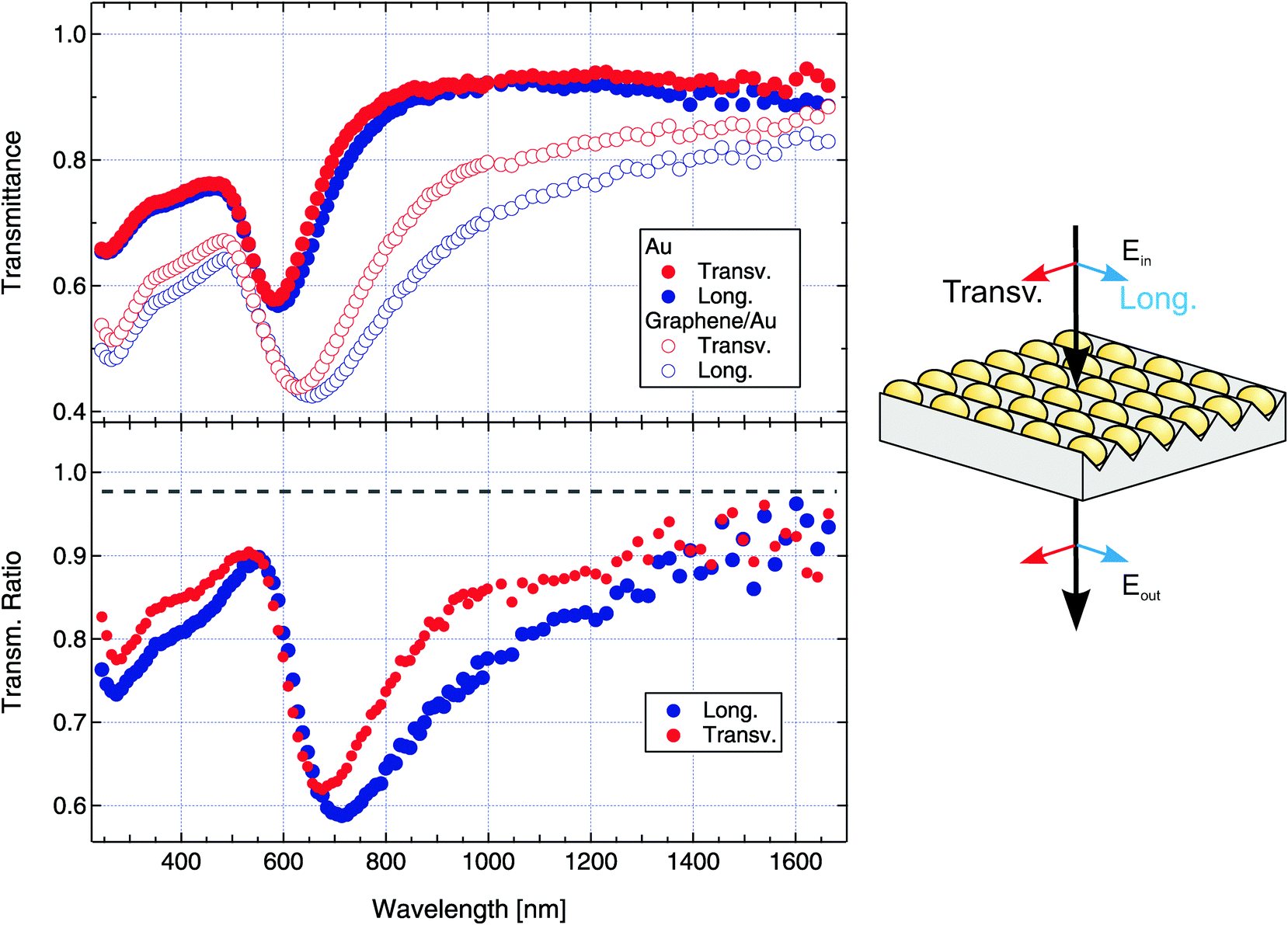 | ||
| Fig. 3 Top graph: Full markers: optical transmittance of the Au-NP arrays in longitudinal (blue) and transverse (red) configurations. Open markers: optical transmittance of the SLG/Au-NP arrays in longitudinal (blue) and transverse (red) configurations. Bottom graph: Ratio R of the optical transmittance of SLG/Au over the Au-only transmittance in longitudinal (blue) and transverse (red) configurations. The dashed black line represents the expected free-standing SLG transmittance (97.7%). Right-hand side: optical geometry for the transmission measurements. | ||
The open markers in the top graph of Fig. 3 represent instead the transmission spectra obtained after the deposition of SLG. Blue (red) open markers represent the L and T configurations, respectively. The LSPR in the L and T configurations is redshifted to wavelengths λL = (655 ± 10) nm and λT = (630 ± 10) nm, respectively, increasing the anisotropy to ΔλL–T ≃ 25 nm. The LSPR peaks significantly broadened, as their FWHM passed from 95 to 155 nm for the L case and from 90 to 120 nm for the T geometry, and the overall transmittance strongly decreased. In the bottom graph of Fig. 3 we report the transmission ratio R defined as the ratio between the transmittance of SLG/Au and the transmittance of bare Au in the pertinent optical geometry. The ratio R immediately allows us to selectively highlight the role of SLG in modifying the optical response of systems. Close to the LSPR, the transmission drops by 35–40%, yielding a ratio R as low as 60%, whereas for wavelengths far from the LSPR (e.g. λ = 1680 nm), R recovers, closely approaching the expected ratio of 97.7% for the addition of non-interacting graphene (R(1680 nm) ≈ 95%),45 implying that the transmittance decrease is strongly correlated with the LSPR excitation. Finally, smaller and sharper dips (corresponding to increased absorption in SLG/Au) appear in R around λ = 275 nm.
3 Discussion
In summary, comparing the transmission spectra before and after the SLG deposition, some remarkable observations can be made. First, the LSPR in both L and T configurations exhibits a graphene induced redshift (55 nm on average) which is remarkably large with respect to literature values.18,25 Secondly, and most importantly, the graphene-induced LSPR variation is strongly anisotropic between L and T configurations, both in terms of LSPR wavelength (ΔλL = 65 nm and ΔλT = 45 nm) and peak width.In chains or arrays of closely spaced plasmonic NPs, the LSPR is a function of both the individual-particle characteristics and the chain/array geometry that dictates the degree of plasmon hybridization.33,46 For given single-particle characteristics, the LSPR may thus vary upon a change of the plasmon hybridization mechanism or intensity. Experimentally, we have observed that the NP morphology and the array geometry are unchanged following the deposition of SLG. This implies that the large and anisotropic LSPR redshift must be due to SLG–NP coupling effects. In this respect, it has been suggested that several mechanisms are potentially able to affect the LSPR of both isolated and near-field-coupled plasmonic nanostructures. First is the polarizability variation of the local NP environment that gives rise to image-dipole charges in graphene with a consequent LSPR redshift.24,25,47 Second, the effect of the plasmonically enhanced EM field leads to locally hot-electron gas in graphene via enhanced photoexcitation: the hot-electron gas locally modifies the NP environment thereby affecting the LSPR.11,12 Last, the injection of plasmonic hot electrons in graphene effectively opens a further non-radiative decay channel for plasmons.27 In the current literature, a debate is still active about what is the actual mechanism responsible for the plasmonic–graphene hybrid system. For isolated (i.e. non EM-interacting) plasmonic systems with large field-enhancement ratios, ref. 12 showed conclusive data about the dominant role of the second mechanism, but the question is still open as to whether this holds for all kinds of plasmonic structures. In discussing our findings, we adopt an open approach assuming that all three interaction mechanisms can potentially affect the behaviour we observe, evaluating their compatibility with the observations.
Starting with environment and image-dipole effects, an inspection of the current literature reveals that this mechanism alone is unable to account for the very large experimentally observed LSPR as redshift values around 10–15 nm have been reported.24
The efficiency of the second mechanism relies on the degree of enhanced photogeneration in graphene due to the plasmonic near fields. In this respect, the systems of ref. 12 exhibited indeed an estimated plasmonic field-enhancement ratio of around 20, which is by all means a considerable value. In our case, the field-enhancement ratio of even higher magnitude is indeed predicted deep inside the interparticle gaps,43 but its value strongly decreases in correspondence of the expected geometrical contact point of NPs and SLG (the top of the nanoparticles), becoming weak and substantially independent of the mutual orientation of incident-polarization and NP chains. Our plasmonic SERS enhancement factor is indeed a mere factor 3.6 implying rather weak field-enhancement ratios within SLG. Under these circumstances, the creation of a high electronic temperature in SLG due to enhanced direct photoexcitation can unlikely represent the dominant mechanism for the graphene/plasmonic interaction and for the large LSPR redshift. Furthermore, it would hardly account for the graphene-induced optical anisotropy, since the plasmonic near-field enhancement within SLG does not exhibit a dependence on the incident-light polarization (ESI†) and very involved mechanisms would thus be required to justify the different efficiencies of indirect graphene heating simply based on its curvature.
In the third scheme, electron transfer between Au NPs and graphene is held responsible for the large LSPR redshift.6,10 The potentially low efficiency of this mechanism, due to the lack of a barrier for re-injection,12 represents a drawback in the case of isolated plasmonic nanostructures but not in our case, since an equilibrium state where electron injection from the NPs into SLG is compensated by an equivalent re-injection will eventually be reached. For the Au NPs in the array, the resistive electronic interaction via graphene48 represents therefore an additional plasmon-hybridization mechanism superimposed to the non-contact EM near-field coupling, that is active even in the absence of SLG. The redshifted LSPR thus represents the new collective resonance condition of the combined SLG/Au system. In the simple framework for which stronger plasmon hybridization implies larger redshifts and a corresponding peak broadening,49,50 the addition of SLG clearly represents a reinforcing mechanism for interparticle interaction.
The resistive-coupling mechanism also lends itself to account for the optical anisotropy in the hybrid system, simply invoking a graphene-curvature dependence of the plasmon hybridization efficiency. The physical grounds for this would be provided by the curvature dependence of electron mobility in SLG,51 where smaller mobilities (increased carrier scattering) are observed transverse rather than parallel to SLG wrinkles.52,53 We notice that this mechanism does not in principle require SLG to be strained in order to occur, and is thus inherently different with respect to a uniaxial-strain modulation of the electrical/optical response. Since the largest redshift is observed in L configuration, corresponding to the electric field along the wrinkles, one can conclude that weaker electron scattering yields stronger graphene-mediated interparticle coupling and vice versa. In this respect, the uniaxial wrinkling of graphene and the anisotropic morphology of the plasmonic NP array allow us to discriminate between dominant and uninfluential interaction mechanisms based on their capability to account for the SLG-induced optical anisotropy.
Finally, we remark that the sharp dips at λ ≃ 275 nm nicely fit with the expected position of the SLG exciton, seldom, if ever, directly observed in simple optical transmission measurements54,55 and here possibly amplified by the interaction with the Au nanostructures.
4 Conclusions
In summary, we have reported the variation of the plasmonic response of an ordered array of closely spaced Au nanoparticles upon deposition of a large sheet of single-layer graphene. The 2D arrays consisted of uniaxially aligned, closely spaced chains of NPs supported on a nanogrooved CaF2 crystal, and exhibited a localized surface plasmon resonance at λ ≈ 590 nm, substantially isotropic as a function of the relative orientation of Au-NP chains and incident light polarization. The arrays are characterized by a very small NP size (11 nm diameter on average) and array pitch (17 nm). Upon laying the SLG sheet onto the Au-NP array, graphene assumed a characteristic uniaxial wrinkling pattern, replicating the substrate uniaxial alignment of Au NPs. The close proximity of the NPs allowed the sheet to be laid on the array without detectable strain. The isotropic plasmonic response of the graphene-free systems strongly redshifted and gave way to a sizable anisotropy upon deposition of SLG. The plasmon resonance for light polarization oriented across the Au-NP chains and across the SLG wrinkles redshifted by 45 nm, whereas the resonance for polarization oriented along the NP chains and the SLG wrinkles redshifted by an amazing 65 nm. The optical transmission of the system decreased by up to 40% in correspondence of the plasmon resonance upon introducing SLG. We ascribed the plasmon-resonance redshift, the optical anisotropy and the strong decrease in transmittance to the strong interaction between graphene and the plasmonic metal. We suggest that the dominant mechanism at play in our system is the coupling of the Au NPs in the system via electron exchange through the SLG. In this framework, a direct correlation exists between the uniaxial wrinkling of graphene and the optical anisotropy, as the degree of coupling between the plasmonic particles, responsible for the resonance redshift, is a function of the SLG conductance, that is in turn influenced by the uniaxial SLG wrinkles.Based on our findings and on the existing scientific literature on graphene–plasmonic interaction, we suggest that the various different coupling mechanisms suggested so far may be simultaneously at play in hybrid systems, but have different weights in determining the overall system response, depending on their specific characteristics. Plasmonic structures where strong field enhancements are promoted in the graphene layer may be more subjected to direct-photoexcitation effects,12 and closely spaced plasmonic resonators may be more affected by resistive coupling through graphene.48 Such a graphene-mediated coupling can in turn be tuned by the graphene nanomorphology that can be manipulated by the presence of suitable substrate nanostructures.
Acknowledgements
Financial support from the Ministero dell'Istruzione, Università e Ricerca (Project no. PRIN 20105ZZTSE_003) is acknowledged. Part of the research leading to these results has received funding from the European Union Seventh Framework Program under grant agreement no. 604391 Graphene Flagship. The image analysis was performed using the open-source software Gwyddion.56References
- K. S. Novoselov, A. K. Geim, S. V. Morozov, D. Jiang, Y. Zhang, S. V. Dubonos, I. V. Grigorieva and A. A. Firsov, Science, 2004, 306, 666–669 CrossRef CAS PubMed.
- K. S. Novoselov, A. K. Geim, S. V. Morozov, D. Jiang, M. I. Katsnelson, I. V. Grigorieva, S. V. Dubonos and A. A. Firsov, Nature, 2005, 438, 197–200 CrossRef CAS PubMed.
- M. L. Brongersma, Faraday Discuss., 2015, 178, 9–36 RSC.
- S. A. Maier, Plasmonics: Fundamentals and Applications, Springer, 2007 Search PubMed.
- A. N. Grigorenko, M. Polini and K. S. Novoselov, Nat. Photonics, 2012, 6, 749–758 CrossRef CAS.
- A. Hoggard, L.-Y. Wang, L. Ma, Y. Fang, G. You, J. Olson, Z. Liu, W.-S. Chang, P. M. Ajayan and S. Link, ACS Nano, 2013, 7, 11209–11217 CrossRef CAS PubMed.
- T. J. Echtermeyer, L. Britnell, P. Jasnos, A. Lombardo, R. Gorbachev, A. Grigorenko, A. Geim, A. Ferrari and K. Novoselov, Nat. Commun., 2011, 2, 458 CrossRef CAS PubMed.
- N. K. Emani, T.-F. Chung, X. Ni, A. V. Kildishev, Y. P. Chen and A. Boltasseva, Nano Lett., 2012, 12, 5202–5206 CrossRef CAS PubMed.
- N. K. Emani, T.-F. Chung, A. V. Kildishev, V. M. Shalaev, Y. P. Chen and A. Boltasseva, Nano Lett., 2014, 14, 78–82 CrossRef CAS PubMed.
- Z. Fang, Y. Wang, Z. Liu, A. Schlather, P. M. Ajayan, F. H. L. Koppens, P. Nordlander and N. J. Halas, ACS Nano, 2012, 6, 10222–10228 CrossRef CAS PubMed.
- Z. Fang, Z. Liu, Y. Wang, P. M. Ajayan, P. Nordlander and N. J. Halas, Nano Lett., 2012, 12, 3808–3813 CrossRef CAS PubMed.
- A. M. Gilbertson, Y. Francescato, T. Roschuk, V. Shautsova, Y. Chen, T. P. H. Sidiropoulos, M. Hong, V. Giannini, S. A. Maier, L. F. Cohen and R. F. Oulton, Nano Lett., 2015, 15, 3458–3464 CrossRef CAS PubMed.
- M. Hashemi, M. H. Farzad, N. A. Mortensen and S. Xiao, J. Opt., 2013, 15, 055003 CrossRef.
- F. H. L. Koppens, T. Mueller, P. Avouris, A. C. Ferrari, M. S. Vitiello and M. Polini, Nat. Nanotechnol., 2014, 9, 780–793 CrossRef CAS PubMed.
- J. Zhu, Q. H. Liu and T. Lin, Nanoscale, 2013, 7785–7789 RSC.
- Y. Yao, M. A. Kats, R. Shankar, Y. Song, J. Kong, M. Loncar and F. Capasso, Nano Lett., 2014, 14, 214–219 CrossRef CAS PubMed.
- D. K. Polyushkin, J. Milton, S. Santandrea, S. Russo, M. F. Craciun, S. J. Green, L. Mahe, C. P. Winolve and W. L. Barnes, J. Opt., 2013, 15, 114001 CrossRef.
- Y. Cai, J. Zhu and Q. H. Liu, Appl. Phys. Lett., 2015, 106, 043105 CrossRef.
- T. Stauber, G. Gómez-Santos and F. J. G. de Abajo, Phys. Rev. Lett., 2014, 112, 077401 CrossRef CAS PubMed.
- X. Zhu, L. Shi, M. S. Schmidt, A. Boisen, O. Hansen, J. Zi, S. Xiao and N. A. Mortensen, Nano Lett., 2013, 13, 4690–4696 CrossRef CAS PubMed.
- S. Heeg, R. Fernandez-Garcia, A. Oikonomou, F. Schedin, R. Narula, S. A. Maier, A. Vijayaraghavan and S. Reich, Nano Lett., 2013, 13, 301–308 CrossRef CAS PubMed.
- F. Schedin, E. Lidorikis, A. Lombardo, V. G. Kravets, A. K. Geim, A. N. Grigorenko, K. S. Novoselov and A. C. Ferrari, ACS Nano, 2010, 4, 5617–5626 CrossRef CAS PubMed.
- P. Wang, W. Zhang, O. Liang, M. Pantoja, J. Katzer, T. Schroeder and Y.-H. Xie, ACS Nano, 2012, 6, 6244–6249 CrossRef CAS PubMed.
- S. G. Zhang, X. W. Zhang, X. Liu, Z. G. Yin, H. L. Wang, H. L. Gao and Y. J. Zhao, Appl. Phys. Lett., 2014, 104, 121109 CrossRef.
- Y. Zhao, X. Li, Y. Du, G. Chen, Y. Qu, J. Jiang and Y. Zhu, Nanoscale, 2014, 11112–11120 RSC.
- G. R. S. Iyer, J. Wang, G. Wells, S. Guruvenket, S. Payne, M. Bradley and F. Borondics, ACS Nano, 2014, 8, 6353–6362 CrossRef CAS PubMed.
- J. Kim, H. Son, D. J. Cho, B. Geng, W. Regan, S. Shi, K. Kim, A. Zettl, Y.-R. Shen and F. Wang, Nano Lett., 2012, 12, 5598–5602 CrossRef CAS PubMed.
- J. C. Reed, H. Zhu, A. Y. Zhu, C. Li and E. Cubukcu, Nano Lett., 2012, 12, 4090–4094 CrossRef CAS PubMed.
- H.-A. Chen, C.-L. Hsin, Y.-T. Huang, M. L. Tang, S. Dhuey, S. Cabrini, W.-W. Wu and S. R. Leone, J. Phys. Chem. C, 2013, 117, 22211–22217 CAS.
- J. Mertens, A. L. Eiden, D. O. Sigle, F. Huang, A. Lombardo, Z. Sun, R. S. Sundaram, A. Colli, C. Tserkezis, J. Aizpurua, S. Milana, A. C. Ferrari and J. J. Baumberg, Nano Lett., 2013, 13, 5033–5038 CrossRef CAS PubMed.
- J. Niu, Y. J. Shin, J. Son, Y. Lee, J.-H. Ahn and H. Yang, Opt. Express, 2012, 20, 19690–19696 CrossRef CAS PubMed.
- L. Gaudreau, K. J. Tielrooij, G. E. D. K. Prawiroatmodjo, J. Osmond, F. J. G. de Abajo and F. H. L. Koppens, Nano Lett., 2013, 13, 2030–2035 CrossRef CAS PubMed.
- L. Anghinolfi, R. Moroni, L. Mattera, M. Canepa and F. Bisio, J. Phys. Chem. C, 2011, 115, 14036 CAS.
- A. Sugawara and K. Mae, J. Vac. Sci. Technol., B: Microelectron. Nanometer Struct.–Process., Meas., Phenom., 2005, 23, 443 CrossRef CAS.
- G. Maidecchi, G. Gonella, R. Proietti Zaccaria, R. Moroni, L. Anghinolfi and F. Bisio, ACS Nano, 2013, 7, 5834 CrossRef CAS PubMed.
- V. Miseikis, D. Convertino, N. Mishra, M. Gemmi, T. Mashoff, S. Heun, N. Haghighian, F. Bisio, M. Canepa, V. Piazza and C. Coletti, 2D Mater., 2015, 2, 014006 CrossRef.
- X. Li, W. Cai, J. An, S. Kim, J. Nah, D. Yang, R. Piner, A. Velamakanni, I. Jung, E. Tutuc, S. K. Banerjee, L. Colombo and R. S. Ruoff, Science, 2009, 324, 1312–1314 CrossRef CAS PubMed.
- A. C. Ferrari, J. C. Meyer, V. Scardaci, C. Casiraghi, M. Lazzeri, F. Mauri, S. Piscanec, D. Jiang, K. S. Novoselov, S. Roth and A. K. Geim, Phys. Rev. Lett., 2006, 97, 187401 CrossRef CAS PubMed.
- A. Das, S. Pisana, B. Chakraborty, S. Piscanec, S. K. Saha, U. V. Waghmare, K. S. Novoselov, H. R. Krishnamurthy, A. K. Geim, A. C. Ferrari and A. K. Sood, Nat. Nanotechnol., 2008, 3, 210–215 CrossRef CAS PubMed.
- Z. Osvath, A. Deak, K. Kertesz, G. Molnar, G. Vertesy, D. Zambo, C. Hwang and L. P. Biro, Nanoscale, 2015, 7, 5503–5509 RSC.
- V. E. Calado, G. F. Schneider, A. M. M. G. Theulings, C. Dekker and L. M. K. Vandersypen, Appl. Phys. Lett., 2012, 101, 103116 CrossRef.
- T. M. G. Mohiuddin, A. Lombardo, R. R. Nair, A. Bonetti, G. Savini, R. Jalil, N. Bonini, D. M. Basko, C. Galiotis, N. Marzari, K. S. Novoselov, A. K. Geim and A. C. Ferrari, Phys. Rev. B: Condens. Matter Mater. Phys., 2009, 79, 205433 CrossRef.
- R. P. Zaccaria, F. Bisio, G. Das, G. Maidecchi, M. Caminale, C. D. Vu, F. De Angelis, E. D. Fabrizio, A. Toma and M. Canepa, ACS Appl. Mater. Interfaces, 2016, 8, 8024–8031 Search PubMed.
- C. J. Shearer, A. D. Slattery, A. J. Stapleton, J. G. Shapter and C. T. Gibson, Nanotechnology, 2016, 27, 125704 CrossRef PubMed.
- R. R. Nair, P. Blake, A. N. Grigorenko, K. S. Novoselov, T. J. Booth, T. Stauber, N. M. R. Peres and A. K. Geim, Science, 2008, 320, 1308 CrossRef CAS PubMed.
- N. J. Halas, S. Lal, W.-S. Chang, S. Link and P. Nordlander, Chem. Rev., 2011, 111, 3913 CrossRef CAS PubMed.
- K. L. Kelly, E. Coronado, L. L. Zhao and G. C. Schatz, J. Phys. Chem. B, 2003, 107, 668 CrossRef CAS.
- B. Thackray, V. G. Kravets, F. Schedin, R. Jalil and A. N. Grigorenko, J. Opt., 2013, 15, 114002 CrossRef.
- P. K. Jain, W. Huang and M. El-Sayed, Nano Lett., 2007, 7, 2080 CrossRef CAS.
- P. Nordlander, C. Oubre, E. Prodan, K. Li and M. I. Stockman, Nano Lett., 2004, 4, 899–903 CrossRef CAS.
- M. Katsnelson and A. Geim, Philos. Trans. R. Soc., A, 2008, 366, 195–204 CrossRef CAS PubMed.
- T. Hallam, A. Shakouri, E. Poliani, A. P. Rooney, I. Ivanov, A. Potie, H. K. Taylor, M. Bonn, D. Turchinovich, S. J. Haigh, J. Maultzsch and G. S. Duesberg, Nano Lett., 2015, 15, 857–863 CrossRef CAS PubMed.
- D. Zhang, Z. Jin, J. Shi, P. Ma, S. Peng, X. Liu and T. Ye, Small, 2014, 10, 1761–1764 CrossRef CAS PubMed.
- F. J. Nelson, V. K. Kamineni, T. Zhang, E. S. Comfort, J. U. Lee and A. C. Diebold, Appl. Phys. Lett., 2010, 97, 253110 CrossRef.
- V. G. Kravets, A. N. Grigorenko, R. R. Nair, P. Blake, S. Anissimova, K. S. Novoselov and A. K. Geim, Phys. Rev. B: Condens. Matter Mater. Phys., 2010, 81, 155413 CrossRef.
- D. Necas and P. Klapetek, Cent. Eur. J. Phys., 2012, 10, 181–188 Search PubMed.
Footnote |
| † Electronic supplementary information (ESI) available: Excitation-polarization-dependent Raman spectra of single-layer graphene. Digital treatment of SEM images for morphological analysis. See DOI: 10.1039/c6cp05107c |
| This journal is © the Owner Societies 2016 |