 Open Access Article
Creative Commons Attribution 3.0 Unported Licence
Acetate ligands determine the crystal structure of CdSe nanoplatelets – a density functional theory study†
Rik S.
Koster
*a,
Changming
Fang
ab,
Alfons
van Blaaderen
a,
Marjolein
Dijkstra
a and
Marijn A.
van Huis
a
aSoft Condensed Matter, Debye Institute for Nanomaterials Science, Utrecht University, Princetonplein 5, 3584 CC Utrecht, The Netherlands. E-mail: r.s.koster@uu.nl; m.a.vanhuis@uu.nl
bBrunel Centre for Advanced Solidification Technology (BCAST), Brunel University London, Uxbridge, Middlesex UB8 3PH, UK
First published on 19th July 2016
Abstract
Cadmium selenide (CdSe) nanoplatelets of a few atomic layers thick exhibit extremely sharp photoluminescence peaks and are synthesized in the zinc blende crystal structure, whereas the most stable bulk polymorph of CdSe is the wurtzite structure. These platelets can be synthesized very monodispersely in thickness, and are covered with acetate ligands. Here, we show by means of density functional theory (DFT) calculations that these ligands play a pivoting role in the stabilization of 2D nanosheets as a whole, including the deviating crystal structure. The relative stability as a function of slab thickness, strong effects on electronic properties, and implications for synthesis are discussed.
Introduction
In the past decade, the interest in two dimensional (2D) nanomaterials has increased dramatically, since these show many desirable physical and electronic properties, often very different from their bulk counterparts. This revolution, which started with graphene,1 now includes a large variety of materials, such as hexagonal boron nitride (h-BN),2,3 metals,4,5 metal oxides,6,7 transition metal dichalcogenides (TMDs)2,8 and semiconductors. Thicknesses of such materials can range from a single atomic layer to tens of atomic layers, while the size in lateral dimensions is at least an order of magnitude larger. Such nanoplatelets, nanosheets or nanomembranes show great promise for applications in flexible electronics, biomedics, optoelectronics, and catalysis.Whereas materials that have a bulk layered crystal structure, e.g. graphene, h-BN or TMD's, can be exfoliated9 to produce 2D nanoparticles, materials that do not have such a structure need to be synthesized by other methods. A frequently used method is using e.g. chemical vapor deposition to produce a thin layer on top of a sacrificial layer, which is subsequently removed leaving the nanosheets freely dispersed. However, this method requires sophisticated equipment, and the lateral dimensions of the resulting particles are difficult to control. A third route is to synthesize nanosheets bottom-up in solution, which allows production of these nanoparticles in larger quantities and achieving more control on their lateral dimensions. The results are highly dependent on the exact chemical details of the synthesis path followed, and currently syntheses are developed on a per case basis, as their underlying mechanisms are often not completely understood. The reader interested in the solution based synthesis methods is referred to the review paper by Wang and Wang.10
One particular system of interest is formed by zinc blende (ZB) cadmium selenide (CdSe) nanoplatelets as recently described by Ithurria and Dubertret.11 The thickness of these platelets is only several atomic layers and can be accurately controlled. The exposed (001) surface is atomically flat, while the lateral 〈100〉 and 〈010〉 directions can extend to roughly 100 nm, depending on the reaction time. The platelets act as 2D quantum wells and show an extremely sharp photoluminescence peak due to quantum confinement,12 making them a suitable candidate material for optoelectronic applications.
Remarkably, the nanoplatelets are synthesized in the ZB structure, whereas wurtzite (WZ) is the most stable bulk CdSe polymorph. This is likely due to the ligands used in the synthesis, although it is excluded that lamellar assembly is the ruling growth mechanism in this case, since the reaction can take place at temperatures too high for lamellar assembly. The presumption that the ligands are of importance was supported by Mahler et al., who showed that replacing carboxylic acids by oleylamine induced a (partial) phase transition in ZB CdSe quantum dots, and a similar effect should be expected here.13
The ligands in these 2D nano materials have a profound influence on their overall stability and physical properties. Therefore, the system as a whole, including ligands, needs to be evaluated quantum mechanically in order to understand why deviating crystal structures, in this case zinc blende (ZB) rather than wurtzite (WZ), are found. To this end, we use density functional theory (DFT) to calculate the total energy, lattice relaxation, and effective charges of relevant configurations, comparing CdSe WZ-(0001), ZB-(001) and ZB-(111) terminations with and without ligand coverage.
Computational methods
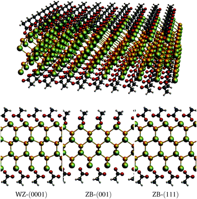
For the DFT calculations, the Vienna ab initio Simulations Package (VASP)14 was used, employing the projector augmented wave method (PAW)15 and the optvdW-B88 functional16 to include non-local van der Waals interactions. The cutoff energy for the wavefunctions was set to 800 eV (1100 eV for the augmentation wavefunctions) and a 22 × 22 × 1 k-point grid was used (Monkhorst–Pack for tetragonal cells, gamma centered for hexagonal cells). Slabs with thicknesses of several atomic layers were used, for each of the surfaces WZ-(0001), ZB-(001) and ZB-(111). Because of the periodic boundary conditions, the slabs extend to infinity in the lateral dimensions. Both the top and bottom side of the slabs were terminated by Cd atoms and a vacuum of at least 22 Å was used. Calculations were done both on bare slabs and on (fully) acetate covered slabs. The structures were allowed to relax until the forces were smaller than 0.03 eV Å−1. Slab thicknesses range from 3 to 11 CdSe layers. Since the slabs are Cd terminated, it implies that an n-layer slab consists of n + 1 Cd layers and n Se layers. For the covered slabs, an acetate molecule is placed on both surface Cd atoms, such that the composition of the cell becomes Cdn+1Sen(CH3COO)2. Fig. 1 shows the relaxed molecular models of the slabs with n = 3.To gain an understanding of the charge distribution of the system, the charge on the atoms, as described by Bader,17 was calculated using the code by the Henkelmann group.18–20 Because the GGA functional is known to underestimate the band gap, the hybrid HSE06 functional as described by Heyd, Scuseria and Ernzerhof was used to investigate the band structure of the most stable configuration.21 For this calculation, the cutoff energy was set to 300 eV (500 for the augmentation wavefunctions), and a mixing parameter α = 0.35 was used, since this value reproduced the WZ bulk band gap at 0 K accurately.
Results and discussion
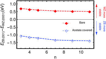
The results of the total energy calculations are listed in Table 1, where energy differences are expressed between ZB slabs and the WZ-(0001) slab, for both the bare and the acetate covered slabs: ΔEBare/Ac(ijk)(n) = EBare/AcZB(ijk)(n) − EBare/AcWZ(0001)(n). The most relevant case, ΔE(001), is also shown in Fig. 2.| n | ΔEBare(001) (eV) | ΔEBare(111) (eV) | ΔEAc(001) (eV) | ΔEAc(111) (eV) |
|---|---|---|---|---|
| 3 | 0.71 | 0.02 | −1.06 | −0.03 |
| 4 | 0.65 | 0.01 | −1.15 | −0.03 |
| 5 | 0.61 | 0.00 | −1.20 | −0.03 |
| 7 | 0.55 | −0.03 | −1.33 | −0.09 |
| 9 | 0.53 | −0.04 | −1.36 | −0.09 |
| 11 | 0.51 | −0.06 | −1.38 | −0.10 |
It is clear that for the uncovered slabs, the energy difference between the ZB-(001) slabs and the WZ-(0001) slabs is positive, i.e. the WZ-(0001) terminated slabs have a much lower energy than the ZB-(001) slabs. As can be expected from the similar crystal structures, the WZ-(0001) and ZB-(111) slabs are similar in energy.
By contrast, the acetate covered slabs have the lowest energy for slabs with the ZB-(001) surface, for all thicknesses calculated. This clearly shows that the stabilization of the ZB-(001) nanoplatelets can be attributed to the adsorption of the acetate ions. Fig. 2 clearly shows that this stabilising effect does not decrease with increasing thickness, at least for the thicknesses of the slabs calculated. Two aspects are of importance here; the number of ligands covering the slabs per unit area and the charge redistribution. First, the adsorption of neighbouring acetate ions might be energetically more unfavourable for WZ slabs than for ZB-(001) slabs, since the surface area per acetate ion is smaller for WZ slabs (16.93 Å2) than for ZB slabs (19.27 Å2). However, we stress that the number of acetate molecules per Cdn+1Sen is the same, so that the energies of slabs with the same thickness can be directly compared. Second, the charge redistribution could be significantly different for the two surfaces. To quantify this, Bader charges were calculated.
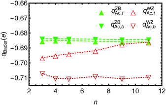
In Fig. 3 and 4 the Bader charges on the acetate ions and the slabs, respectively, are shown. The charge transfer from the zinc blende(001) slab to the acetate ions is approximately 0.685 e, for both the top and the bottom acetate ion, due to symmetry, and irrespective of the slab thickness. It is clear that the WZ(0001) slabs show a larger charge on the acetate ions. Moreover, since there is no mirror symmetry in the xy-plane, the charge on the bottom acetate differs somewhat from the charge on the top slab.
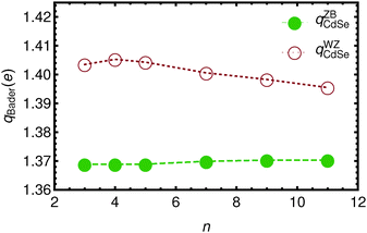 | ||
| Fig. 4 The total Bader charge on the Cdn+1Sen slabs a function of n. Open circles denote the WZ-(0001) slabs, while solid circles represent the ZB-(001) slabs. Lines are drawn to guide the eye. | ||
For a more qualitative description of the charge redistribution, isosurfaces of the electron density difference δρ are plotted in Fig. 5. Here, δρ is defined as
δρ(![[r with combining right harpoon above (vector)]](https://www.rsc.org/images/entities/i_char_0072_20d1.gif) ) = ρslab+2Ac( ) = ρslab+2Ac(![[r with combining right harpoon above (vector)]](https://www.rsc.org/images/entities/i_char_0072_20d1.gif) ) − ρslab( ) − ρslab(![[r with combining right harpoon above (vector)]](https://www.rsc.org/images/entities/i_char_0072_20d1.gif) ) − ρAc,top( ) − ρAc,top(![[r with combining right harpoon above (vector)]](https://www.rsc.org/images/entities/i_char_0072_20d1.gif) ) − ρAc,bottom( ) − ρAc,bottom(![[r with combining right harpoon above (vector)]](https://www.rsc.org/images/entities/i_char_0072_20d1.gif) ), ), | (1) |
![[r with combining right harpoon above (vector)]](https://www.rsc.org/images/entities/i_char_0072_20d1.gif) ) is the electron density obtained for a static calculation of only the CdSe slab, and ρAc,top/bottom(
) is the electron density obtained for a static calculation of only the CdSe slab, and ρAc,top/bottom(![[r with combining right harpoon above (vector)]](https://www.rsc.org/images/entities/i_char_0072_20d1.gif) ) the electron densities of only the top/bottom acetate molecule. This effectively shows how the electrons are redistributed due to the acetate molecule covering the surface. Isosurfaces at δρ(
) the electron densities of only the top/bottom acetate molecule. This effectively shows how the electrons are redistributed due to the acetate molecule covering the surface. Isosurfaces at δρ(![[r with combining right harpoon above (vector)]](https://www.rsc.org/images/entities/i_char_0072_20d1.gif) ) = ±0.03 are shown in Fig. 5. The oxygen atoms show a net gain in electron density, with an increase directly above the O atoms and a (smaller) decrease at the O position. Consequently, the Cd atom covered by the acetate shows a net decrease in electron density, with an increase directly at the Cd position and a (larger) decrease in the area above it. For the bottom WZ acetate, the charge redistribution seems to extend to the Se atom in the subsurface layer.
) = ±0.03 are shown in Fig. 5. The oxygen atoms show a net gain in electron density, with an increase directly above the O atoms and a (smaller) decrease at the O position. Consequently, the Cd atom covered by the acetate shows a net decrease in electron density, with an increase directly at the Cd position and a (larger) decrease in the area above it. For the bottom WZ acetate, the charge redistribution seems to extend to the Se atom in the subsurface layer.
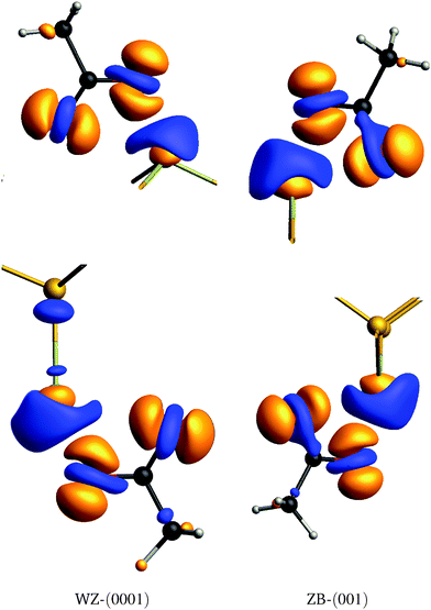 | ||
| Fig. 5 Electron density differences δρ at the top and bottom of the slabs. Isosurfaces δρ = 0.03 Å−3 (orange) and δρ = −0.03 Å−3 (blue) are shown. | ||
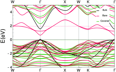
In the ESI† the projected densities of states (pdos) are shown for the bare and covered slabs. The off-stoichiometry has introduced states at the Fermi energy for both bare slabs and the WZ covered slab, making these slabs conducting instead of semi-conducting. Since the CdSe ZB-(001) slabs are the most relevant, the band structure was calculated using the hybrid HSE06 functional. Fig. 6 shows a bandgap of 2.35 eV for the acetate covered slabs, which is in very good agreement with the observed photoluminescence peaks at 2.42 eV.22,23 The bare slab mid-gap states, which consist mostly of outer layer Cd s-orbitals and selenium p-orbitals, disappear in the covered slab; the states in either the conduction or the valence band do not show such a strong contribution from the outer layer Cd atoms. The significant difference between the band structures of the bare and covered slabs show that it is essential to take the ligands into account when determining the electronic structure of this system.
We have shown by DFT calculations that the acetate ions play an essential role in stabilising the ZB structure for CdSe nanoplatelets. It should be noted however that all these DFT calculations are necessarily limited to the total energy calculations of small systems. They do not take into account the effect of the solvents or other molecules present, and neglect entropy effects as they are done at 0 K. To explain the synthesis in full detail, the dynamics of the system must be understood. DFT calculations are not suitable for this and accurate MD simulations that would be required for that purpose are left for future work.
Conclusion
In summary, our DFT calculations show that indeed the absorption of stabilizing acetate ions onto CdSe nanoplatelets is responsible for the stabilization of the ZB crystal structure, even for nanoplatelets up to 11 layers thick. The ligands are crucial in determining the stability of this 2D nanomaterial as they induce a particular charge redistribution at the surface. The band gap for the most stable nanoplatelet that we calculated using the hybrid HSE06 functional is in excellent agreement with the energy of the experimentally observed photoluminescence. Our findings have considerable implications for a wide range of other 2D nanomaterials that are growth controlled by ligand manipulation, in particular those that are synthesized in an unusual crystal structure.24Acknowledgements
M. A. v. H. acknowledges the Dutch science foundation NWO for a VIDI grant (grant number 723.012.006).References
- K. S. Novoselov, A. K. Geim, S. V. Morozov, D. Jiang, Y. Zhang, S. V. Dubonos, I. V. Grigorieva and A. A. Firsov, Science, 2004, 306, 666–669 CrossRef CAS PubMed.
- K. S. Novoselov, D. Jiang, F. Schedin, T. J. Booth, V. V. Khotkevich, S. V. Morozov and A. K. Geim, Proc. Natl. Acad. Sci. U. S. A., 2005, 102, 10451–10453 CrossRef CAS PubMed.
- A. Pakdel, Y. Bando and D. Golberg, Chem. Soc. Rev., 2014, 43, 934–959 RSC.
- X. Huang, S. Tang, X. Mu, Y. Dai, G. Chen, Z. Zhou, F. Ruan, Z. Yang and N. Zheng, Nat. Nanotechnol., 2011, 6, 28–32 CrossRef CAS PubMed.
- J. Niu, D. Wang, H. Qin, X. Xiong, P. Tan, Y. Li, R. Liu, X. Lu, J. Wu, T. Zhang, W. Ni and J. Jin, Nat. Commun., 2014, 5, 3313 Search PubMed.
- Z. Sun, T. Liao, Y. Dou, S. M. Hwang, M.-S. Park, L. Jiang, J. H. Kim and S. X. Dou, Nat. Commun., 2014, 5, 3813 CAS.
- T. Sasaki, M. Watanabe, H. Hashizume, H. Yamada and H. Nakazawa, J. Am. Chem. Soc., 1996, 118, 8329–8335 CrossRef CAS.
- V. Sorkin, H. Pan, H. Shi, S. Y. Quek and Y. W. Zhang, Crit. Rev. Solid State Mater. Sci., 2014, 39, 319–367 CrossRef CAS.
- V. Nicolosi, M. Chhowalla, M. G. Kanatzidis, M. S. Strano and J. N. Coleman, Science, 2013, 340, 1420 CrossRef CAS.
- F. Wang and X. Wang, Nanoscale, 2014, 6, 6398–6414 RSC.
- S. Ithurria and B. Dubertret, J. Am. Chem. Soc., 2008, 130, 16504–16505 CrossRef CAS PubMed.
- S. Ithurria, M. D. Tessier, B. Mahler, R. P. S. M. Lobo, B. Dubertret and A. L. Efros, Nat. Mater., 2011, 10, 936–941 CrossRef CAS PubMed.
- B. Mahler, N. Lequeux and B. Dubertret, J. Am. Chem. Soc., 2010, 132, 953–959 CrossRef CAS PubMed.
- G. Kresse and J. Furthmüller, Comput. Mater. Sci., 1996, 6, 15–50 CrossRef CAS.
- P. E. Blöchl, Phys. Rev. B: Condens. Matter Mater. Phys., 1994, 50, 17953–17979 CrossRef.
- J. c. v. Klimeš, D. R. Bowler and A. Michaelides, J. Phys.: Condens. Matter, 2010, 22, 022201 CrossRef PubMed.
- R. F. W. Bader, Atoms in Molecules – A Quantum Theory, Oxford University Press, Oxford, 1990 Search PubMed.
- G. Henkelman, A. Arnaldsson and H. Jónsson, Comput. Mater. Sci., 2006, 36, 354–360 CrossRef.
- E. Sanville, S. D. Kenny, R. Smith and G. Henkelman, J. Comput. Chem., 2007, 28, 899–908 CrossRef CAS PubMed.
- W. Tang, E. Sanville and G. Henkelman, J. Phys.: Condens. Matter, 2009, 21, 084204 CrossRef CAS PubMed.
- J. Heyd, G. E. Scuseria and M. Ernzerhof, J. Chem. Phys., 2003, 118, 8207–8215 CrossRef CAS.
- M. Olutas, B. Guzelturk, Y. Kelestemur, A. Yeltik, S. Delikanli and H. V. Demir, ACS Nano, 2015, 9, 5041–5050 CrossRef CAS PubMed.
- L. Biadala, F. Liu, M. D. Tessier, D. R. Yakovlev, B. Dubertret and M. Bayer, Nano Lett., 2014, 14, 1134–1139 CrossRef CAS PubMed.
- W. van der Stam, Q. A. Akkerman, X. Ke, M. A. van Huis, S. Bals and C. de Mello Donega, Chem. Mater., 2015, 27, 283–291 CrossRef CAS.
Footnote |
| † Electronic supplementary information (ESI) available: Density of states plots for CdSe slab calculations. See DOI: 10.1039/c6cp04935d |
| This journal is © the Owner Societies 2016 |

