
 Open Access Article
 This Open Access Article is licensed under a
 Creative Commons Attribution 3.0 Unported Licence
Quantitative parameters for the examination of InGaN QW multilayers by low-loss EELS
Alberto
Eljarrat
 *a,
Lluís
López-Conesa
a,
César
Magén
b,
Noemí
García-Lepetit
c,
Žarko
Gačević
c,
Enrique
Calleja
c,
Francesca
Peiró
a and
Sònia
Estradé
a
*a,
Lluís
López-Conesa
a,
César
Magén
b,
Noemí
García-Lepetit
c,
Žarko
Gačević
c,
Enrique
Calleja
c,
Francesca
Peiró
a and
Sònia
Estradé
a
aLENS-MIND-IN2UB, Laboratory of Electron NanoScopies, Departament d'Electrónica, Universitat de Barcelona, Barcelona, Spain. E-mail: aeljarrat@el.ub.edu
bLMA-INA Laboratorio de Microscopías Avanzadas, Instituto de Nanociencia de Aragón – ARAID, Departamento de Física de la Materia Condensada, Universidad de Zaragoza, 50018 Zaragoza, Spain
cISOM, Instituto de Sistemas Optoelectrónicos y Microtecnología, Universidad Politécnica de Madrid, Madrid, Spain
First published on 2nd August 2016
Abstract
We present a detailed examination of a multiple InxGa1−xN quantum well (QW) structure for optoelectronic applications. The characterization is carried out using scanning transmission electron microscopy (STEM), combining high-angle annular dark field (HAADF) imaging and electron energy loss spectroscopy (EELS). Fluctuations in the QW thickness and composition are observed in atomic resolution images. The impact of these small changes on the electronic properties of the semiconductor material is measured through spatially localized low-loss EELS, obtaining band gap and plasmon energy values. Because of the small size of the InGaN QW layers additional effects hinder the analysis. Hence, additional parameters were explored, which can be assessed using the same EELS data and give further information. For instance, plasmon width was studied using a model-based fit approach to the plasmon peak; observing a broadening of this peak can be related to the chemical and structural inhomogeneity in the InGaN QW layers. Additionally, Kramers–Kronig analysis (KKA) was used to calculate the complex dielectric function (CDF) from the EELS spectrum images (SIs). After this analysis, the electron effective mass and the sample absolute thickness were obtained, and an alternative method for the assessment of plasmon energy was demonstrated. Also after KKA, the normalization of the energy-loss spectrum allows us to analyze the Ga 3d transition, which provides additional chemical information at great spatial resolution. Each one of these methods is presented in this work together with a critical discussion of their advantages and drawbacks.
1 Introduction
Devices based on the stacking of III–V semiconductor layers have led to a revolution in the optoelectronic research and industrial fields because of their ability to operate in a wide range of applications. Among these applications, high brightness light emitting diode (LED) devices based on multiple InxGa1−xN quantum well (QW) active layers are important because of their high quantum efficiency.1,2 There is a strong need to control the QW thickness down to the monolayer level while keeping a high indium composition, in order to achieve optimum operating properties.The reduction of the QW size, down to the nanometer range, is difficult to control due to strain accumulation at the InGaN/GaN interfaces. It is also problematic to achieve a high indium content, given the tendency of InxGa1−xN compounds towards phase separation. For instance, indium mobility is an issue and some authors have reported indium coalescence during growth in similar systems.3–9 In some of these studies,4–7 the formation of segregated In-rich nanoclusters, with an In content of above 80%, has been reported. In other cases,8,9 some inhomogeneity inside the InGaN QW, and width variations have been observed. Variations in both the local In composition and the QW width have been related to a carrier localization effect in the InGaN QW regions.10 In these devices, carrier localization improves recombination rates, notwithstanding the typically high threading dislocation densities, which, in turn, act as light-quenching centers. Consequently, this effect could be responsible for the high emission rates obtained in InxGa1−xN heterostructure-based laser devices.11
In the present work, we aim to give a detailed account of useful models to characterize group-III nitride heterostructures at the nanometer scale using scanning transmission electron microscopy (STEM) methods; electron energy loss spectroscopy (EELS) and high angle annular dark field (HAADF) imaging. As the properties of these devices depend on structural features in the nanometer size range, TEM represents a unique tool because of its outstanding spatial resolution. The use of electron microscopy to resolve crystalline structures up to the atomic level as well as the analytical capabilities offered by its different operating modes is well established. Among these, the STEM mode is much appreciated because of its ability to focus a sub-nm sized electron probe onto a given area of the studied sample. This paper is centered on the quantitative information that can be extracted from locally acquired energy-loss spectra. The scope of our work is the analysis of the chemical and electronic properties of semiconductors through a typical STEM acquisition. From the examination of the low-loss region of EELS and high resolution HAADF images, we obtain complementary quantitative information following various strategies. The advantages and drawbacks of these different approaches are revealed by a critical comparison of their results and theoretical models.
1.1 Theoretical background
EELS is a technique routinely performed in TEM that analyzes the kinetic energy of the fast electrons in the beam after transmission through a thin film sample. As the initial energy of these electrons is known, given by the microscope operating voltage, one obtains an energy-loss spectrum; i.e., the integrated scattering distribution entering the detector, I(E), where E is the energy-loss relative to the initial energy.Energy-loss spectroscopy in the region 0–50 eV, below the excitation threshold for most core inonization edges, is typically referred to as the low-loss EELS region. Inelastic scattering in low-loss EELS is dominated by electron excitation processes whose initial state is in the valence band, with broad energy ranges. Hence, low-loss EELS can potentially measure the fundamental properties of semiconductor materials, like the band gap and other interband transitions. Apart from these single electron excitations, collective excitation effects, such as surface and bulk plasmons, are also present in low-loss EELS. Typically, the (bulk) plasmon peak is the most intense feature in EELS, apart from the zero-loss peak (ZLP). Note that while the ZLP carries little chemical information, the plasmon peak is directly related to the composition of the material and has been exploited in group-III nitride compound semiconductors.12–16Fig. 1a shows a typical low-loss EELS spectrum from InxGa1−xN, which includes the mentioned features.
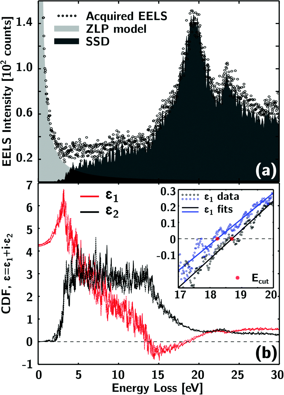 | ||
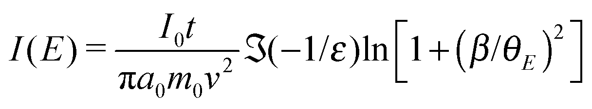
| Fig. 1 (a) Example of the energy-loss spectrum of InxGa1−xN. This panel shows the effect of our data treatment as it depicts the ZLP model (light gray) subtracted by deconvolution from the original spectrum (circles) to obtain the SSD (dark gray). The features analyzed in this work are: the band gap, which is expected at ∼3 eV; the plasmon, the most intense peak at ∼19 eV; and the Ga-3d transition at ∼22.5 eV. (b) Two CDFs obtained after KKA of EELS acquired at the InGaN barrier (solid lines) and QW (dashed lines) layers. In the inset, the detail of the 17–20 eV region, showing the ε1 fit process, to obtain Ecut is provided. The data from the barrier are in black and from the QW in blue. Note the shift in Ecut (red crosses). | ||
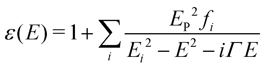
It is advantageous to invoke the dielectric formulation to link the experimental low-loss EELS intensity, I(E), with the optical response properties of a material expressed in a complex dielectric function (CDF), ε(q,E) = ε1 + iε2. In the framework provided by the dielectric theory, the energy lost by the fast electrons can be calculated as the work exerted back by the induced electric field, with wave-vector q and frequency ω = ℏE, over the bound charge distribution of the material medium. By using a semi-classical approximation for single scattering in the low-q limit, considering an isotropic medium, and keeping only the bulk loss term from a slab of thickness, t, I(E) is found to be proportional to the inverse of the CDF, ℑ(−1/ε), termed the energy-loss function (ELF). The expression is as follows:17
 | (1) |
The main advantage of this formalism is that the quantum theory realm is bound within the CDF, and thus provides a qualitative relationship between features in a given spectrum and material properties derived from calculations, such as density functional simulations.12 In the low-q scattering limit, the CDF is in principle determined as a result of the additive contribution of independent elemental excitations.18,19 Consider, for the sake of simplicity, an isotropic semiconductor crystal: because all the occupied states lie in the valence band below the Fermi energy, only interband transitions, with binding energies, Ei, are allowed. Then, the CDF can be phenomenologically formulated using simple equations, such as the Lorentz oscillator model:20
 | (2) |
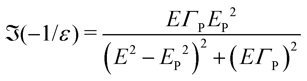 | (3) |
In this work, we use Kramers–Kronig analysis (KKA), which allows us to retrieve the CDF from EELS measurements, when I(E) is adequately treated. This treatment is explained in detail elsewhere,15,17 and only a rough summary of the procedure follows. In the first step, this treatment requires the suppression of plural scattering, e.g. by Fourier-log deconvolution. Note that electrons in I(E) may have been inelastically scattered more than once, an effect which increases with the thickness of the sampled region, but only the single scattering distribution (SSD) is modeled by eqn (1). After this is done, it is customary to acquire the ZLP intensity and have an approximate knowledge of the refraction index, n, in order to normalize I(E) using eqn (1) to obtain the ELF. Finally, the semi-relativistic formalism leading to eqn (1) also allows us to calculate the non-retarded surface plasmon contribution to EELS, which is routinely excluded from I(E) in KKA through iterative subtraction.
Once the CDF has been calculated, additional information from bulk electronic properties may be obtained. For example, one can estimate the electron effective mass, m*, related to charge mobility, following the formula for the free-electron plasmon energy,26
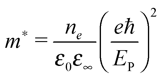 | (4) |
Another interesting study on similar samples proposed the examination of the Ga 3d transition in ε2,28 in order to quantify the concentration of this metal. In the present work, we improve on this method by examining the same transition in a previously normalized SSD. We show how this normalization can be done after KKA, based on eqn (1), revealing the gallium concentration distribution with an excellent spatial resolution.
As already introduced, it is possible to directly measure the band gap energy from the low-loss EELS.15 For semiconducting materials with a direct band gap between nearly parabolic bands, like GaN and InN, this signal presents a characteristic square root shape 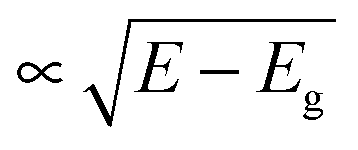 , and is recognizable as the spectral feature with the lowest energy threshold. Nevertheless, in the above presentation of the dielectric formalism, we have disregarded radiative contributions to the bulk and surface losses. In most real operation cases, these have a non-negligible impact, that can thwart the interpretation of the low energy features.17,29 In the worst case scenario, the combined impact of both spurious signals may distort the true band gap signal shape. An extended formalism to include a full-relativistic description of the fast electron beam provides a straightforward way to compute the scattering probability from the CDF.15,24,30 However, the KKA-like reverse computation from I(E) is not yet feasible given the complexity of the involved equations. It is thus advisable to use results from first principles calculations or dielectric information from other techniques (e.g. optical measurements) in order to gain a deeper understanding of the obtained EELS data. In this work, the low energy features in our experimental EELS were assessed through such full-relativistic calculations.
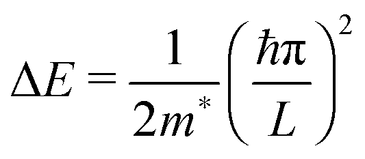
For band gap and also for plasmon energies, a size dependent shift is expected in these small structures. As the size of the QW shrinks it is customary to consider a quantum confinement model to assess the band structure related properties. A simple one is given in ref. 19, for a free particle with effective mass, m*, confined in one direction by impenetrable barriers with a known separation, L. In this simple case, the increase in ground state energy for that particle, ΔE, is
 | (5) |
Finally, delocalization of inelastic scattering in these energy ranges is important and can be the leading cause for plasmon broadening in the vicinity of some interfaces. The electron probe in a STEM–EELS experiment can be as small as 1 Å, and one may expect low-loss spectra to originate from interactions with an atomic-sized volume of the sample material. However, it is generally accepted that this realization is far from reality due to the finite range of electron interaction and the extended nature of elemental excitations, particularly low-loss excitations.31 Because the threshold energy for the transitions in valence EELS is low, the characteristic Coulomb delocalization is increased. Importantly, for the band gap and other features at low energy-loss (but also for the plasmon excitation), the effective characteristic length may become much larger than the probe size.17
2 Experimental details
The multiple QW heterostructure under study was grown in a RIBER Compact 21 Molecular Beam Epitaxy (MBE) system, equipped with a radio-frequency plasma nitrogen source and standard Knudsen cells for Ga and In, on commercial ∼3.3 μm GaN-on-sapphire (0001) templates (Lumilog), grown by metal organic chemical vapor deposition. Prior to InxGa1−xN quantum wells (QWs), an ∼20 nm thick In0.05Ga0.95N spacer was grown. Afterwards, six 1.5 nm thick InGaN QWs with a nominal In content of 20% were grown. The InGaN QWs are separated by 6 nm thick InGaN quantum barriers and covered with a 20 nm thick InGaN capping layer, both layers with a nominal 5% In content. The entire growth was performed under intermediate metal-rich conditions and without interruption, to facilitate good crystal quality and formation of flat and abrupt interfaces (for growth details see ref. 32).To get preliminary insight into the layer structural properties, X-ray diffraction (XRD) was performed. The samples were assessed using the Cu-Kα1 line (λX = 1.5406 Å), in a commercial Panalytical X'Pert Pro system, equipped with a Ge(220) hybrid monocromator. Meanwhile, the sample optical properties were assessed by photoluminescence (PL) measurements, exciting using a HeCd laser (λ = 325 nm) with a power density of ∼1 W cm2 at ∼10 K and room temperature (RT).
Thin lamella specimens were prepared for TEM observation using standard techniques of mechanical polishing, dimpling and low angle Ar-ion milling. The cross-section geometry was used, in which the c-axis is perpendicular to the electron beam. In this configuration, the compositional gradients defining the different layers and the interfaces between them become apparent in TEM observation.
STEM experiments were performed using a probe corrected FEI Titan 60–300 microscope operated at 300 kV and equipped with a CEOS aberration corrector for the condenser system achieving a spatial resolution of <1 Å. For EELS analysis, this instrument combines a high-brightness Schottky field emission gun (X-FEG), a Wien Filter gun monochromator, and a Gatan Tridiem ERS 866 energy filter/spectrometer to provide an energy resolution better than 0.2 eV. We used the spectrum imaging (SI) technique, in which the small STEM probe rasters a rectangular region of the sample, acquiring pixel-by-pixel spatially localized EELS (estimated probe size below 0.2 nm) simultaneously with the HAADF signal. In this way, the spectroscopic information can be easily correlated with the structural features of the region of interest.
Additionally, high resolution HAADF images were acquired because of their ability to portrait the structure with atomic resolution and Z-contrast. The inclusion of the relatively large indium atoms will produce a more intense scattering at high angles, giving away the position of In-rich regions. This information is typically used to assess the crystalline quality of the sample and to locate the position of the InGaN QW and barrier layers.33 Beyond that we performed geometric phase analysis (GPA) of the images to quantify the lattice deformation of the crystalline structure.34
The low-loss EELS-SI were treated using computational tools available in the open-source Hyperspy Python package.35 To improve the spectral signal-to-noise ratio (SNR), we used a spatial filtering approach (see Fig. 1). First, cross-correlation of the ZLP was used to calibrate the energy axis. After that, averaging and deconvolution methods were used in order to subtract the tails of the ZLP and to effectively improve the SNR. To perform the averaging, we applied a square uniform spatial filter (3 × 3 pixel size). At the same time, we used Richardson–Lucy deconvolution (RLD), a Bayesian algorithm that uses a ZLP model to increase spectral resolution.36 Using this method, we obtain an improvement in spectral resolution from ∼0.3 eV to ∼0.16 eV, measured by the FWHM of the ZLP. Additionally, RLD also reduced the tail of the ZLP, which masks low-energy features like the band gap onset. Finally, ZLP and plural scattering were suppressed by the Fourier-log deconvolution (FLD).15
This data processing improves the SNR at the expense of the spatial resolution of the datasets, originally below 1 nm. Here, we have taken into account that we are examining valence properties with a certain delocalization length, e.g. on the order of 1 nm for the plasmon. By repeating all the following calculations using unfiltered datasets, we made sure that no important information was sacrificed when increasing the SNR and removing artifacts from the spectra in this manner. After the processing, we obtained a pixel-by-pixel map of the single scattering distribution (SSD). Band gap, plasmon and interband transition signals were measured in the SSD using the model-based fit procedures explained in ref. 15, 16 and 28.
3 Results and discussion
3.1 Preliminary structural and optical characterization: XRD and PL
Preliminary structural information about the sample under study has been obtained by ω/2Θ XRD scans around the (0002) GaN Bragg reflection (Fig. 2a). The XRD spectrum reveals satellite peaks, resolved up to the third order. The satellite peak separation confirms a structure with a high periodicity, with the period thickness found to be 7.5 nm, in excellent agreement with the nominal QW (1.5 nm) and barrier (6 nm) values.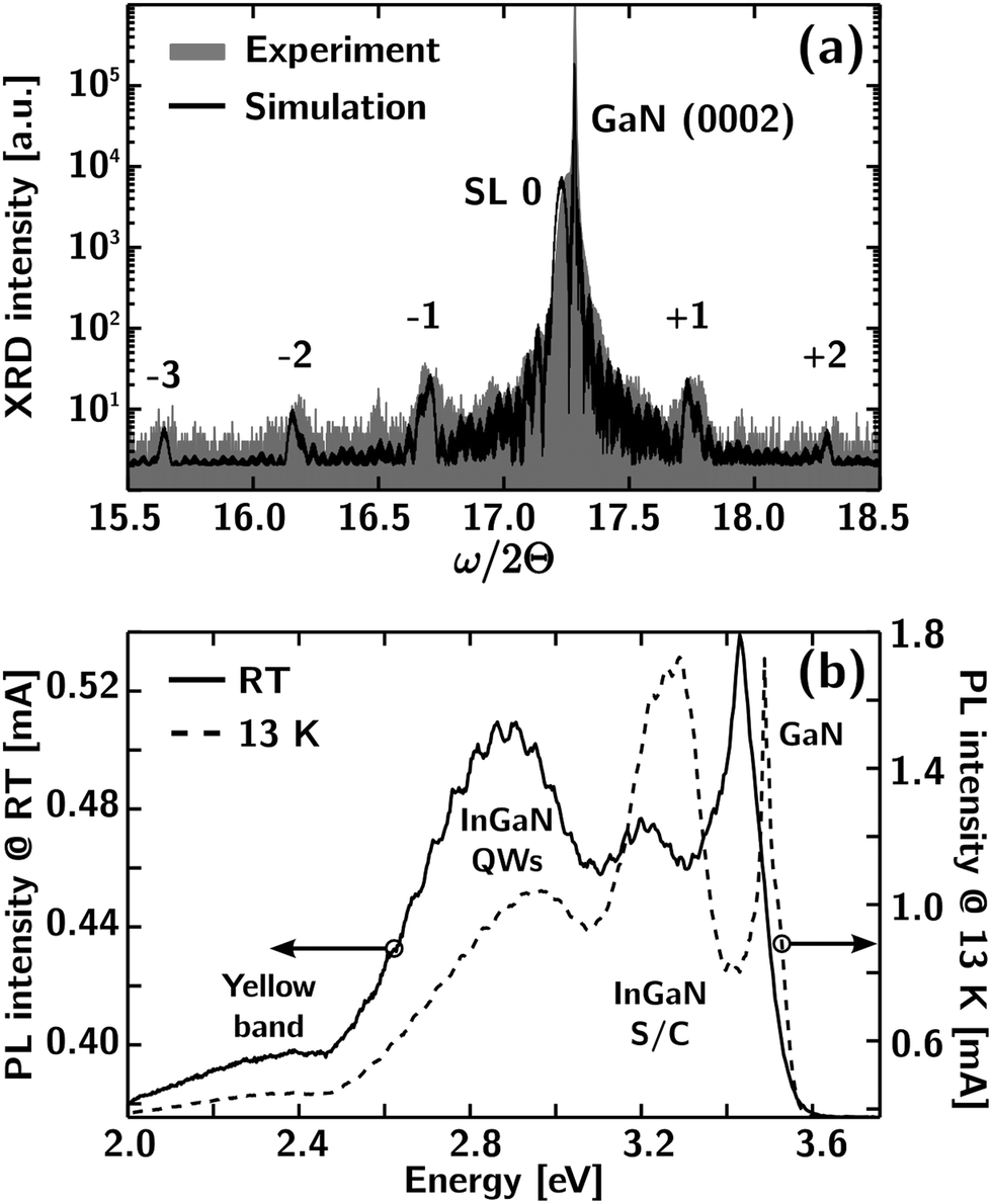 | ||
| Fig. 2 (a) An XRD line-scan and the simulated intensity from a structural model; depicted by a gray filled area and a solid line, respectively. The simulation confirms the growth of a superlattice structure. (b) PL spectra acquired at room temperature (RT) and at 13 K; depicted with solid and dashed lines, respectively. The peaks are identified with the band gap from the GaN substrate and the InGaN QW structure. | ||
PL measurements, in Fig. 2b, performed at 13 K, reveal three intense emission peaks, attributed to the underlying GaN, InGaN spacer/capping and InGaN QWs, respectively (from high to low energy). The energy of the InGaN QWs and InGaN spacer/capping is found to be in good agreement with their nominal 20 and 5% In contents, respectively. The increase in temperature leads to a certain emission red shift and intensity drop (note that the two spectra are plotted with different scales), as expected. The relative intensity of InGaN QW emission (defined as the integrated emission intensity of InGaN QWs versus the total integrated emission intensity), is nevertheless, higher at room temperature than at low temperature. This behavior, commonly observed for these types of structures,37,38 is attributed to the thermally enhanced mobility of photo-excited carriers, which consequently reach the InGaN QWs (i.e. the lowest energy emission band) more easily.
3.2 QW structural examination and strain analysis: high resolution HAADF
Owing to the use of the Cs-corrector, the resolution of the HAADF images obtained allows us to measure the lattice parameters of the crystalline layers. Z-Contrast in these images means that the inclusion of the relatively large indium atoms will produce more intense scattering at high angles, revealing the position of the InGaN QW layers. This information is used to assess the crystalline quality of the sample and to locate the position of the barrier and QW layers. Fig. 3 shows an example of a high-resolution HAADF image; it corresponds to an InGaN QW. The width of the QW in this image is near the nominal value of 1.5 nm, with parallel and abrupt interfaces.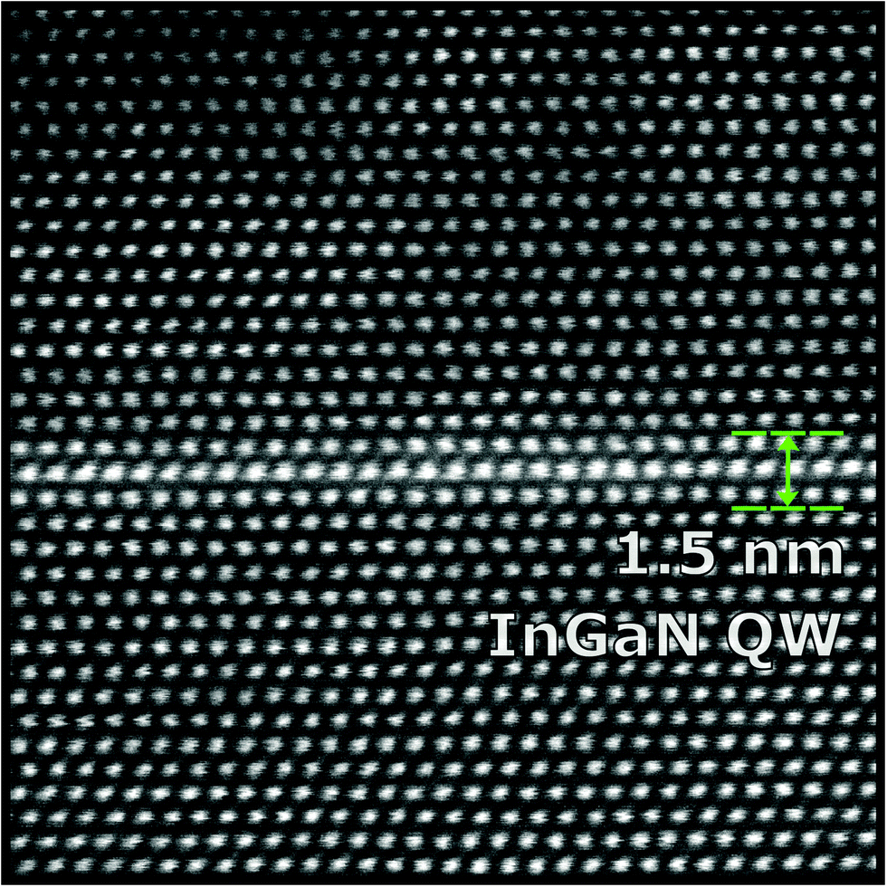 | ||
| Fig. 3 A high resolution HAADF image of the InGaN multilayer portraying a QW region (bright contrast in the central region) and two barrier layers (dark contrast regions, above and below). The nominal width of the QW region, 1.5 nm, is indicated with dashed lines and an arrow. | ||
Fig. 4 shows another high-resolution HAADF image, this time at a lower magnification, including several periods of the multilayer structure. In this image, we can still resolve the crystalline atomic columns and assess the location of the InGaN QW layers, identified by their brighter contrast. This allows the measurement of the width of the periods in the repeating QW and barrier multilayer structure, which is in excellent agreement with the nominal value of 7.5 nm. We can also assess the inhomogeneity of the QW layers, with bulgings extending a few nanometers in some regions. The formation of these wider inhomogeneities is always detected at the upper QW interface, which is typically rougher than the lower one, in good agreement with the previous observations for similar systems.14,39,40
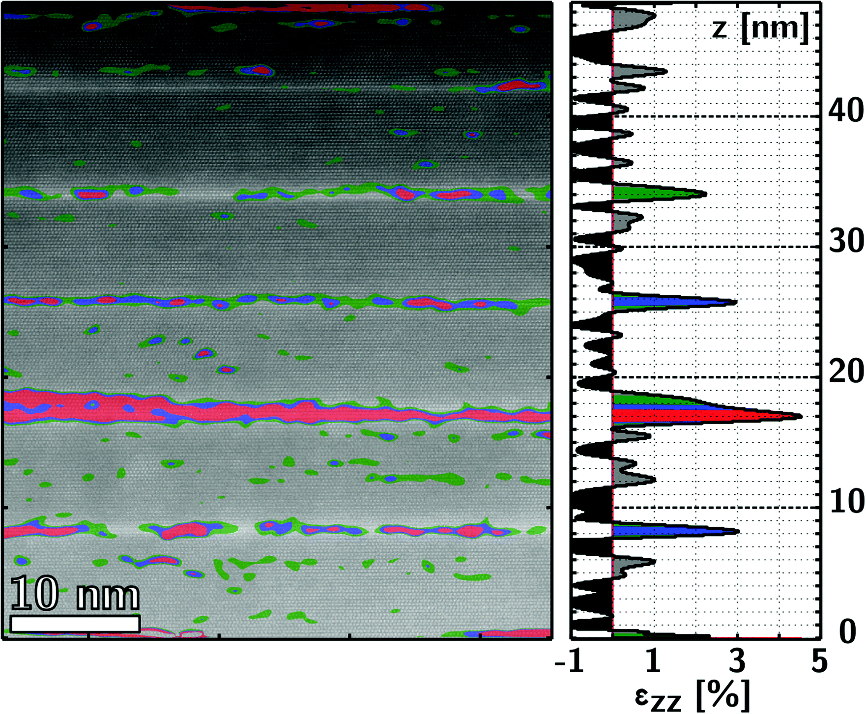 | ||
| Fig. 4 A high resolution HAADF image with color filled contours showing the out-of-plane strain matrix element (εzz) resulting from the GPA calculation. The average values of εzz can be examined in the plot on the right hand side. | ||
In these images, the bright Z-contrast is indicative of the substitution of lighter gallium atoms for heavier indium ones. As the layers grow epitaxially, keeping the wurtzite structure, we expect a certain level of strain to be present in the crystalline structure.8 In order to explore the strain distribution in this lattice from HAADF images we have used GPA software.34 GPA calculates the relative spatial deformation maps from an image of a crystalline lattice using Fourier transforms. For this purpose, it is necessary to define a reference region in the image. The result of GPA is a map showing the spatial dependence of the elements of the strain matrix, ε, which measures the lattice deformation relative to the reference region.
Fig. 4 also contains the information obtained from this analysis. In the GPA calculation, the lower region from the HAADF image was selected as a reference. It corresponds to a 20 nm InGaN spacer layer with a nominal In composition of 5%, which in principle should be more stable than the adjacent multilayer structure. GPA maps only show an appreciable strain in the out-of-plane direction. This direction corresponds to the c lattice parameter in the wurtzite structure, which we are going to call the z direction; thus, the lattice strain is expressed in the εzz matrix term. This term is shown in Fig. 4 using green, blue and red filled contours for increasing values of strain. Additionally, the right-side graph in Fig. 4 shows the average strain in the vertical direction of the whole image. By looking at this graph and the contours, we observe that the higher values of this εzz term are located in the InGaN QW layers.
The inclusion of more indium atoms is related to an increase of the out-of-plane lattice parameter (εzz > 0).8,11,33,40,41 For this and other types of III–V semiconductor alloys, it is natural to explain this in terms of the Vegard law. In this framework, a linear relationship is formulated between the measured lattice parameter of the alloy and the lattice parameter of the pure components, as a function of composition. If biaxial strain is also taken into account in wurtzite InxGa1−xN,41 an equation allows the extraction of x from experimentally determined a and c lattice-parameters. Using this equation, we first calculated x for the lattice parameter in the spacer layer, (a, c) = (0.319, 0.522) nm, measured by analyzing the FFT in this region. We obtained a concentration of x = 0.05, in excellent agreement with the nominal value. Considering this result, we continued using this equation to assess the indium concentration through the strain map in Fig. 4, which gives the deformation in the c lattice-parameter. Consequently, the detected strain values above 2.5% correspond to an indium content of 20%, above the nominal indium composition in the QW layers. Moreover, lattice deformations of around 5% correspond to an indium content of ∼35%. Such large lattice deformations are consistently detected in our HAADF images, in the regions showing a wider bulging of the QW. Conversely, intermediate strain values (below 2%) are detected for the QW layers, close to the nominal value of 1.5 nm. Finally, the GaN barrier regions show more moderate strain (below 1%) at the detection limit for this analysis.
Other authors have reported deformations above 10%, indicating an indium content of ∼80%, for similar systems in which In-clustering had been observed.4–7 Our results, and the homogeneous Z-contrast of the HAADF images indicate that, if present, a more moderate degree of indium diffusion is occurring in this particular system. Anyway, when preparing this work we were aware of the reports stating that In-cluster formation may be induced by the high irradiation damage in typical HRTEM experiments.8,11,42 In those cases, InGaN samples containing similar QW heterostructures present an indium segregation and separation of phases that is detectable by examination of time series images. However, recent studies have postulated that a comparatively small amount of irradiation damage is suffered by InGaN in a typical HR-STEM observation.33 Moreover, this adds to the fact that no particular In-cluster formation was detected during our STEM acquisition, for example, through salt-and-pepper or dot-like contrasts, which we surveyed by acquiring images of the same regions through the whole experimental process. Because of this, we relate the detected εzz gradients to the natural lattice deformation induced during the growth process.
3.3 Measurement of the band gap energy
Using the data treatment explained in Section 2, the SSD is retrieved after deconvolution of the ZLP from the original spectrum, as depicted in detail in Fig. 5a, and the features at low energy-loss are revealed. We assume that the band gap signal is at the lowest energy-loss (here ∼3 eV). The validity of this assumption was assessed by the simulation of the EELS intensity using a full-relativistic inelastic scattering calculation for an 80 nm GaN slab (the measured relative thickness, t/λ, is below 0.9 for the examined regions). These calculations were carried out as explained in ref. 15, with the difference that these time optical data were used as input;43 results are shown in Fig. 5b.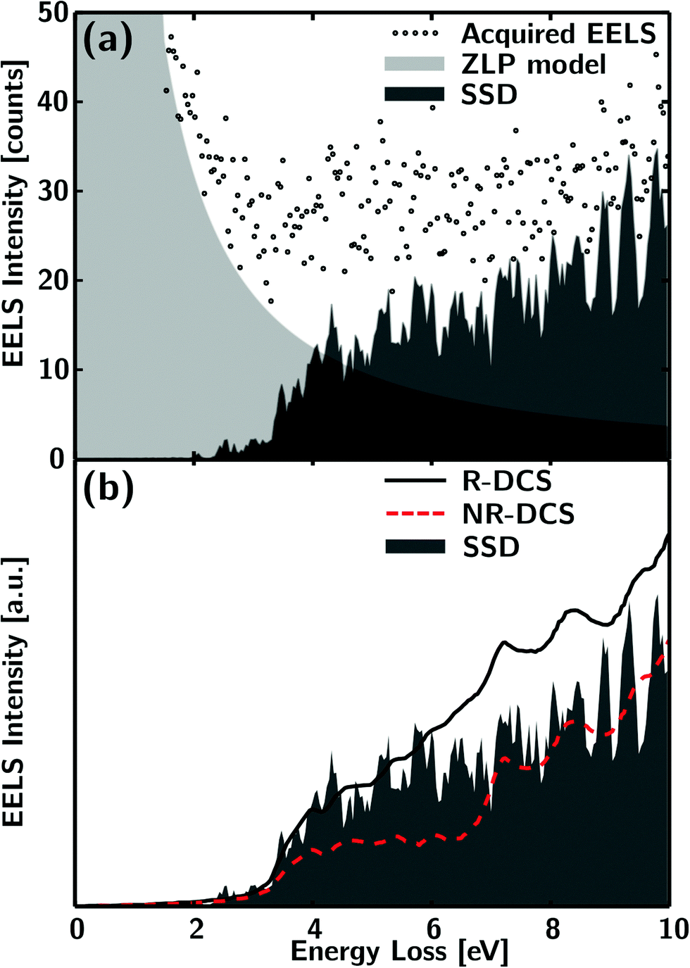 | ||
| Fig. 5 (a) Detail from the 0–10 eV energy-loss region as in Fig. 1. (b) The same SSD is compared with the results from a full-relativistic calculation, performed with optical data.43 These results are the relativistic differential cross-section (DCS), black solid line, and the non-relativistic DCS, red dashed line. | ||
We first note that the experimental and simulated intensities near the signal onset are in good agreement up to ∼6 eV (see Fig. 5b, black solid line). Above that energy, both intensities diverge a little, as the simulation predicts an increase of the relativistic contribution. The origin of this divergence is in the relativistic surface-loss term of the calculation, rather than in the bulk radiative-loss. Hence, the departure can be related either to a failure to estimate surface effects, or, rather, a failure of the optical data (from ref. 43) to predict high-energy dielectric behavior. Nevertheless, the result confirms that the characteristic square root shape for the direct band gap transition is the dominant contribution to the spectral intensity below 10 eV. Moreover, we are now convinced that, for our experimental thickness and beam energy, the contributions from surface and radiative losses are not intense enough as to mask the other low-energy features.
The three panels in Fig. 6b depict two QW periods, both with suspected In-diffusion regions. The InGaN QWs are apparent in the HAADF image of the same region, thanks to Z-contrast, allowing the identification of the origin of the energy-loss spectra in the simultaneously acquired EELS-SI. Spatially resolved band gap onset energy values were obtained from the inflexion points at low energies (between 1 and 10 eV), in each spectra. The inflexion points were calculated using a normalized and smoothed derivative of the spectrum, obtained from a Savitzky–Golay filter. This procedure results in energy values of around 3.1 ± 0.1 eV, as depicted in Fig. 6a (red filled histogram). The band gap onset energy for InxGa1−xN upon the first approximation is linearly related to the band gap energy of the pure compounds. The generally accepted values for these energies are 3.44 eV and 0.77 eV,44–46 for pure bulk GaN and InN, respectively. Following the Vegard law, our average band gap energy value corresponds to an indium concentration, x, of around 12.4%. Remarkably, these band gap energy/concentration values are between, and close to the mean of the nominal values for the InGaN barriers and QW layers, of 3.3 eV/5% and 2.9 eV/20%, respectively.
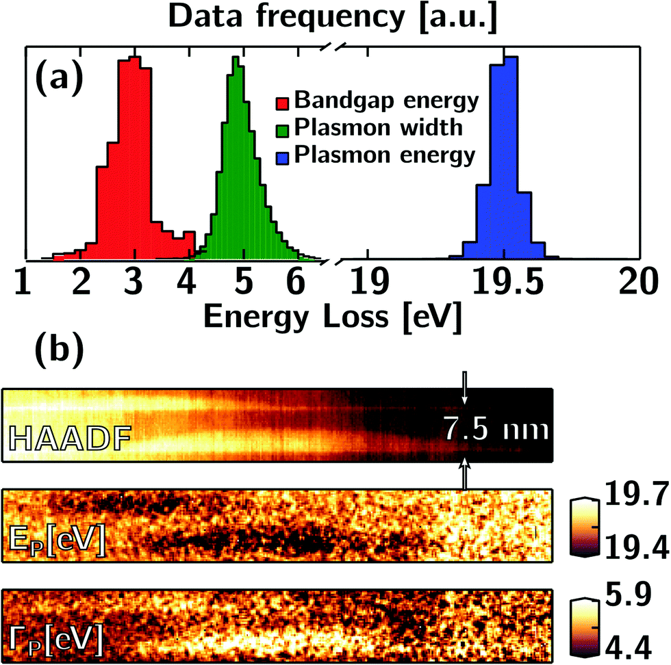 | ||
| Fig. 6 (a) Histogram showing the dispersion of the inflexion energy (bin size 0.2 eV), ΓP, and EP (bin size 0.1 eV); in red, green and blue color filled areas, respectively. The band gap was measured using the inflexion method, as explained in the text. (b) From top to bottom, the HAADF image and maps for EP and ΓP, from the same region. The spatial resolution was ∼0.3 nm. | ||
In the pure compounds, both band gaps are direct transitions.12,19,23,47 In EELS, the energy dependence of the signal in direct transitions is as SSD  near the signal onset. A fit based on a model containing this square root function has confirmed this type of band gap in our spectra. This fitting procedure could be carried out throughout the whole spectrum image, giving an equivalent result to that obtained above for the onset energy. However, the inflexion-point procedure proved to be more reliable, giving a much smaller dispersion of values.
No spatial correlation with the InGaN QW position was found, neither using the inflexion point procedure nor using the model-based fit. We have to consider that spatial delocalization for this interaction is larger than the dimensions of the multilayer structure constituents.12,48 Hence, these extremely thin QW layers are effectively rendered invisible to the direct detection of their band gap properties using a fast electron beam. Given the beam spreading and delocalization lengths for the band gap signal it is reasonable to think that the electron beam interacts with both the InGaN barrier and QW layers as a whole.22 Arguably, the band gap energy that has been observed is related to an average band gap signal of the layered system. This is in contrast with the results obtained by similar studies,8 in which In-clusters of around 3 nm in size presented a sizable band gap onset energy redshift to around 2.65 eV. This different result could be related to a bigger size and higher indium concentration of the In-clusters in the samples analyzed in that work.
Finally, taking into account the reduced size of the InGaN QW layers, quantum confinement effects could be taking place. Because of that, an increase of the band gap energy, of ≲1 eV for a 1.5 nm wide QW (see eqn (5)), is expected in these layers, which is not detected. Following the discussion in the last paragraph, trying to assess the impact of this effect by monitoring the band gap alone seems hopeless given the large delocalization of this signal.
3.4 Plasmon analysis
Our interest now is in the plasmon peak and the interband transitions, features appearing at higher energy-loss than the band gap. After a Drude model-based fit procedure is applied pixel-by-pixel to our EELS-SI,16 plasmon energy, EP, and width, ΓP, values are measured (see eqn (3)). Fig. 6b presents these results as histograms and maps, compared with the simultaneously acquired map of the HAADF intensity. From an examination of the histograms, in panel (a), it becomes apparent that the dispersion of the plasmon energy and width values is smaller than for the inflexion energy values resulting from the study of the band gap region. From the maps, we see that the spatial distribution of the plasmon energy and width shows some contrast in the QW region. Additionally, the HAADF image shows this region and confirms that acquisition has not suffered much from spatial drift.Plasmon energy measurement across the QW and barrier layers yields quite constant values. Only a slight variation range of 0.2 eV is found, between the wider QW regions and the barrier layers, at about 19.4 eV and 19.6 eV, respectively. Additionally, a localized broadening of the plasmon peak in the InGaN QW layers is detected. ΓP shows a wider change range between InGaN QWs and barrier layers of around 1 eV.
Parts of the InGaN QW structures are almost invisible by looking at the plasmon energy distribution. As for the band gap, delocalization of the plasmon interaction is an important factor that needs to be addressed. In this sense, we have to take into account that the delocalization length for the plasmon interaction is ∼1 nm. The nominal size of the QW structure, 1.5 nm, is on the order of this length. On the other hand, for localized QW regions with larger size well above 3 nm at their most prominent bulging, a consistent plasmon energy and a width change range are apparent. Then, it is reasonable to conclude that these measures correspond to characteristic properties of these objects.
The determination of the indium concentration in the multilayer structure from these plasmon measurements is a controversial matter. For instance, following a linear Vegard law, considering that for the pure compounds, EGaNP = 19.7 eV and EInNP = 15.7 eV, the obtained  in the InGaN barrier layers would be of x ≃ 2.5%, an indium content half the nominal value. However, the InxGa1−xN system has been reported to follow a parabolic version of the Vegard law with a negative bowing parameter, as in ref. 49 for the band gap (b = −1.43 eV), and ref. 9 for the plasmon (b = −2.55 eV). In this sense, b ≃ −2.1 eV would suffice to get the nominal In composition of 5% in the InGaN barrier layers. The value of b in ref. 9 would indicate indium incorporation in the barrier layers above the nominal concentration.
The measured plasmon energy for the QW layers, around 19.4 eV, deserves a final comment, as it is far too large for In0.2Ga0.8N. In a hypothetical system of broader layers with the same nominal composition, a larger negative gradient of the plasmon energy in the In-rich regions, of several eV, would be expected.9 Again, one has to consider the impact of nanometer size effects, increasing the ground energy by an amount, termed the confinement energy, proportional to the inverse square of the barrier separation (see eqn (5)). As a consequence, both the band gap and the plasmon energies may experience an increase of ΔE ≲ 1 eV for barriers separated by L ≲ 1.5 nm.
With the available information, it is difficult to determine which effect is responsible for the broadening of the plasmon peak. So far we have showed that plasmon broadening is sizable in the thin InGaN QW layers, whereas the plasmon energy shift is undetectable in these regions. Other studies showed plasmon broadening independent of the energy shift in similar systems with strained layers.16 It thus seems that these two facts support the evidence of a strain driven broadening at a scale similar to the plasmon delocalization length, through the enhancement of de-excitation processes. Nevertheless, the QC effect has also been related to a significant broadening of the plasmons,50,51 as well as the already considered delocalization and strain effects.
3.5 Kramers–Kronig analysis
Kramers–Kronig analysis (KKA) was carried out on the SSD spectrum images, in order to further explore the electronic properties of the InGaN structure. Before using the KKA algorithm a standard pretreatment procedure was used to taper the SSD intensity at high and low energies.15 This procedure is important for the numerical stability of the KKA algorithm, which uses fast Fourier transforms (FFTs). These are prone to errors when the spectral intensity at the energy extrema does not decay smoothly down to zero. Care was taken to suppress only the intensity at low energies (below the band gap) proceeding from the remaining signal after ZLP tail subtraction, which is mostly noise without any specific physical meaning. This is dealt with using a Hanning taper to filter the data in this region along the energy dimension. The intensity at high energy comes from the plasmon tail and the limited energy range used to acquire it. We use a power law fit to smoothly extend this decaying tail up to the next power of two, another important factor in the success of the KKA algorithm.Once the SSD spectrum image was treated, a standard KKA algorithm was used to calculate the complex dielectric function (CDF).15,17 This calculation relays on prior knowledge of the refraction index, n, of the material under observation. Precise knowledge of n in a nanostructure is unlikely, except for notable exceptions.52,53 For our multilayer structure we lacked this knowledge, but we assumed we could approximate the CDF by using the known refractive index of pure GaN, nGaN = 2.4,12 given the relatively low indium concentration. This assumption is supported by the fact that EELS measurements in these regions show only quite subtle variations from those in the barrier regions. In doing this we estimate that QW regions do not differ strongly in their optoelectronic properties from the rest of the multilayer. A complex dielectric function (CDF), ε(E), is obtained from each energy-loss spectrum in the EELS-SI. Additionally, an estimation of the absolute thickness, t, of the sampled region is obtained, yielding ∼80 nm, in good agreement with the estimation we made from t/λ. A t map was also obtained, which is presented later in the next subsection.
A closer look at an InGaN QW region, with greater spatial resolution, is presented in Fig. 7. A smaller bulging, of about ∼3 nm at its widest, is visible in the HAADF image. The contrast from this QW region is also apparent in the EP map. The contrast in this map is faint, yet an additional region of lower EP values appears at the top of the image. Because of its position, we know that this region is not part of the next QW period, but rather some localized inhomogeneity in the adjacent barrier.
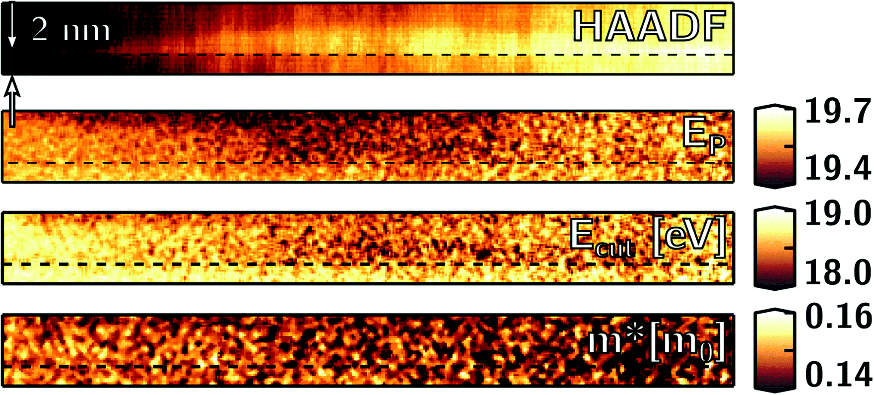 | ||
| Fig. 7 From top to bottom, the HAADF image, EP, Ecut and m* maps, from an InGaN QW region. Note that the growth direction is from bottom to top, and a dashed line is included in all images to indicate the start of the QW deposition. All images are the result of the same SI acquisition, for which the pixel size was 0.2 nm. | ||
After the KKA of this spectrum image was performed, we explored the calculation of spatially resolved properties. For instance, the zero-cut energy of the CDF, Ecut, was determined through a linear fit of the real part of the CDF in the 17–20 eV energy region, as depicted in Fig. 1. Fig. 7 shows a map of Ecut together with a map of EP, for comparison. The EP map was obtained through the model based fit procedure explained above. These plasmon energy maps show a contrast along the QW and in the indium diffusion region above it. Additionally, Ecut seems to have an amplified contrast of ∼1 eV, greater than the ∼0.3 eV one, which we can see in the EP map.
The good agreement between Ecut and EP was already expected, as both properties are related to the collective mode excitation. On the one hand, the determination of EP from the SSD, through model based fitting, relies on the quasi-free particle approximation in eqn (3). This model can fail to predict the true shape of the plasmon peak in EELS to some extent, because of the presence of interband transitions (see eqn (2)). On the other hand, plasmon energy determination through Ecut does not rely on a model and still gives a measure of the energy for collective transitions. To our knowledge, this approach has not been exploited in the low-loss EELS literature.
Fig. 8 shows the ΓP map, extracted from the same analysis as EP in Fig. 7, in which a broadening of the plasmon is again observed, localized around the InGaN QW layer. Moreover, the contrast in this map extends along most of the QW, even through thinner parts (see dashed line).
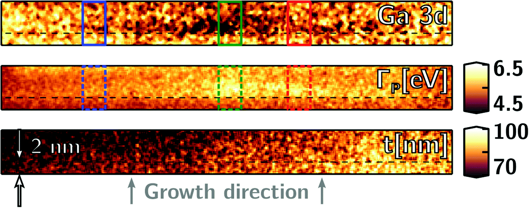 | ||
| Fig. 8 From top to bottom, the Ga 3d intensity, ΓP and t maps are from the same region as in Fig. 7. Ga 3d is an integral mapping, subjected to normalization; hence, in this case no intensity bar is given. Additionally, three color squares over the Ga 3d and ΓP are used to indicate the regions from which the averages in Fig. 9 were taken. | ||
3.6 Electron effective mass mapping
We also mapped the electron effective mass, m*, using the plasmon energy (EP) maps and the CDFs (see eqn (4)). To perform this calculation, we previously calculated and combined the effective density of electrons at the valence excitation, neff, and the infinite-frequency dielectric function, ε∞.27 The obtained m* map for the EELS-SI (also in Fig. 7) shows values between 0.16m0 and 0.14m0. The expected m* values for the conduction of electrons for the binary compounds are mGaN* ∼ 0.2m0 and mInN* ∼ 0.11m0, where m0 is the electron rest mass.19 For an InxGa1−xN compound, we expect the value to typically lie between 0.2m0 and 0.11m0. In terms of absolute values, the agreement of our calculations with the theoretically expected values is good. We detect somehow lower values associated with the presence of wider In-rich regions in the QW at the center of the image, but there is not enough information to confirm a consistent spatial distribution of this effect.
3.7 Ga 3d intensity
In addition to the characterization of the plasmon, we also examined the Ga 3d transition intensity. Before this could be done, we needed a method to normalize the spectral intensity, so that it could be used for approximate elemental quantification. In the developed method, we take advantage of the absolute thickness, t, map obtained from KKA. This map is included at the bottom in Fig. 8, and portraits the thickness gradient in the region. Using this knowledge and the ZLP total intensity, I0, we can normalize the SSD following eqn (1). Because in this equation the angular term varies slowly for energies above ∼10 mrad, this procedure ensures that the intensity in a normalized SSD is proportional to ℑ(−1/ε). Note that the angular factor can be calculated and added if necessary, for instance, if using a wider integration energy window. We expect the integral of the intensity below the Ga 3d transition to be proportional to the gallium concentration, following the Bethe f-sum rule.17,28To extract the spectral intensity of the Ga 3d transition, routine background subtraction on the normalized SSD-SI was performed, using a power-law fit before ∼21.5 eV. The Ga 3d intensity is found in the 22–25 eV spectral range. The intensity integral in this range is shown in the top panel of Fig. 8. To calibrate the image we used the average over the first nm in the growth direction (see arrow in the left hand side), that presented a relatively homogeneous intensity distribution. Hence, this region was normalized to 95% gallium, the nominal composition of the barrier. Square regions are marked in Fig. 8, using color-coded rectangles. Average line profiles in these regions, through the in-plane direction, were taken from the Ga 3d and ΓP maps. These profiles are portrayed in Fig. 9 with solid and dashed lines, respectively.
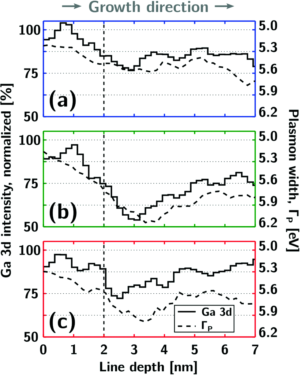 | ||
| Fig. 9 In panels (a–c), the Ga 3d intensity (solid lines) and ΓP (dashed lines) averaged from the blue, green and red rectangular regions highlighted in Fig. 8. As in that figure, an arrow indicates the growth direction, from left to right, and the dashed line indicates the start of the QW. | ||
The maps and profiles of the Ga 3d intensity inform us of the composition of the examined InxGa1−xN region. Panels (a) and (b) in Fig. 9 (solid lines), showcase the left-hand side and central regions of InGaN QW bulging. Both profiles indicate the depletion of gallium where the QW was deposited, with a width of ∼1.5 nm in (a) and ∼3 nm in (b). In the central region the depletion is deeper, the Ga 3d intensity drops to almost 50% of its maximum value, at the wider part of the bulge. The profiles indicate some localized diffusion region above the QW: gallium concentration in the region after the deposition of the InGaN QW is much smaller than in the region before. In contrast, panel (c) from the right-hand side region shows an abrupt start of the QW valley, 1.5 nm wide, and a lower degree of indium diffusion. The quantification of the profiles indicates that InxGa1−xN composition at the sides of the QW is close to x = 0.2 (gallium concentration of 80%), and in the central part of the bulge the composition is closer to x = 0.5. It seems that the right-hand side region returns somewhat to the Ga 3d intensity level at the beginning of the next period. Meanwhile, the other regions keep a low Ga 3d intensity, indicative of gradual diffusion. The origin and the extent of this effect are hard to precisely identify from this transmission measurement taking into account the presence of a sizeable thickness gradient (see Fig. 7). Finally, a region further above the QW shows compositional inhomogeneity according to the Ga 3d intensity. Note that this region is a localized spot inside the barrier region, not visible in the HAADF image.
The examination of the Ga 3d transition was initially proposed in ref. 28, in similar samples, characterizing also the ε1 shift and intensity. In our work, the possibilities of using ε1 was naturally explored, as we performed KKA. As expected, we obtained similar maps as for the normalized SSD intensity ones, but, with an increased numerical noise which we were not able to improve. Indeed, the analysis of the SSD is advantageous in the sense that it is performed directly from EELS measurement without the need for model-based fitting to ε1. Anyway, the success of this method relies on our ability to normalize the SSD to produce spectra effectively proportional to ℑ[1/ε]. This is only possible if the thickness gradient is small (or better, negligible), as was our case. In cases where thickness gradients are important, using ε1 may be advantageous, if KKA is still feasible.
In summary, for the InGaN QW and some localized spots inside the barriers, we have measured the shift and broadening of the plasmons. See for instance Ecut in Fig. 7, in which a consistent plasmon energy shift is detected for the QW, and also at a separate spot on top of the image, in the barrier region. Meanwhile, the ΓP map in Fig. 8 and profiles in Fig. 9 (dashed lines), show broadening of the plasmon peak in these two regions. These measurements follow a similar trend to the Ga 3d intensity (solid lines), indicative of a gradual indium diffusion from the QW, as already commented. Note that this analysis is in overall good agreement with the strain analysis by GPA. It has been suggested that broadening of the plasmon peak may serve as an indicator of strain in nanoscaled systems.25 Indeed, out-of-plane deformation has been related to the broadening of the plasmon peak before.13
It is hard to give a precise estimation of the magnitude of indium diffusion to the barriers, although evidence from the 3d Ga intensity and Z-contrast in the HAADF images suggests that it is small and occurs at localized spots. In the localized region on top of Fig. 7, the HAADF contrast is not as bright as for the QW. Additionally, the strain analysis from GPA shows that the overall structural inhomogeneity inside the barriers is negligible.
4 Conclusions
We have presented an STEM characterization of a multiple InxGa1−xN QW structure, with QW size at the resolution limit of the low-loss EELS technique. Atomic resolution HAADF imaging has been used to observe the QW and barrier layers, using Z-contrast and GPA strain analysis to obtain structural and chemical information. These analyses reveal the accumulation of out-of-plane strain and indium species above the nominal concentration in the QWs, forming wider bulging of these layers. Since such changes are expected to alter the electronic properties of these materials, we have proceeded with the examination of low-loss EELS. In order to produce a consistent quantitative characterization, we have analyzed all data in the framework of the dielectric formulation. We have also taken into account the strong spatial delocalization and possible quantum size effects affecting the low-loss EELS measurements, for these structures with sizes in the nanometer range.After measuring the band gap energy onset, Eg, in EELS-SIs, we have found that the QW features are virtually undetectable with no spatial distribution of the values. Indeed, a larger delocalization length is expected for this signal. However, the average Eg value has also been related to the mean indium content in these layers through the Vegard Law. Additionally, we have compared our measurements with optical data using full-relativistic calculations of the EELS intensity.
The plasmon peak has been also analyzed, using a model-based fit technique to measure its energy (EP) and width (ΓP). A consistent shift and broadening of this peak in the InGaN QW layer were detected, with spatial resolution near to the QW size range. However, the obtained EP values are well above the expectation for the suspected QW composition, which we relate to a quantum confinement effect. Moreover, ΓP maps exhibit higher contrast and spatial resolution, which can also be related to the structural and chemical inhomogeneity in the layers.
In addition, we have proposed other quantitative parameters that can be accessed using the same EELS data, after KKA. For instance, the direct determination of the collective mode energy threshold as Ecut in ε(Ecut) = 0 has been demonstrated. The results from this procedure seem to improve the plasmon energy contrast in the QW, in relation to model-based plasmon shift measurement. Other measurements after KKA, electron effective mass (m*) and absolute thickness (t), have also been presented. These m* measurements have been related to the expected values for the pure binaries.
Finally, we have shown how, after normalization of the SSD, chemical information can be obtained by examination of the Ga 3d transition. Maps of the intensity of this transition have been obtained with a strong contrast in the QW regions. These gradients can be related to gallium depletion in the In-rich QW regions. They confirm the chemical information extracted from HAADF and plasmon measurement.
Acknowledgements
We acknowledge the financial support from the Spanish Ministry of Economy and Competitivity via the Consolider: IMAGINE (CSD2009-2013) and MAT2013-41506. TEM facilities at CCiT-UB and LMA-INA are also acknowledged.References
- S. Nakamura, Science, 1998, 281, 956–961 CrossRef CAS.
- S. Nakamura, M. Senoh, N. Iwasa and S. Nagahama, Jpn. J. Appl. Phys., 1995, 34, L797 CAS.
- I. Ho and G. B. Stringfellow, Appl. Phys. Lett., 1996, 69, 2701–2703 CrossRef CAS.
- C. Kisielowski, Z. Liliental-Weber and S. Nakamura, Jpn. J. Appl. Phys., 1997, 36, 6932 CrossRef CAS.
- D. Gerthsen, E. Hahn, B. Neubauer, A. Rosenauer, O. Schön, M. Heuken and A. Rizzi, Phys. Status Solidi A, 2000, 177, 145–155 CrossRef CAS.
- D. Gerthsen, E. Hahn, B. Neubauer, V. Potin, A. Rosenauer and M. Schowalter, Phys. Status Solidi C, 2003, 1668–1683 CrossRef CAS.
- Y.-C. Cheng, E.-C. Lin, C.-M. Wu, C. Yang, J.-R. Yang, A. Rosenauer, K.-J. Ma, S.-C. Shi, L. Chen and C.-C. Pan, et al. , Appl. Phys. Lett., 2004, 84, 2506–2508 CrossRef CAS.
- J. Jinschek, R. Erni, N. Gardner, A. Kim and C. Kisielowski, Solid State Commun., 2006, 137, 230–234 CrossRef CAS.
- K. H. Baloch, A. C. Johnston-Peck, K. Kisslinger, E. A. Stach and S. Gradečak, Appl. Phys. Lett., 2013, 102, 191910 CrossRef.
- Z. Li, J. Kang, B. Wei Wang, H. Li, Y. Hsiang Weng, Y.-C. Lee, Z. Liu, X. Yi, Z. Chuan Feng and G. Wang, J. Appl. Phys., 2014, 115, 083112 CrossRef.
- C. J. Humphreys, Philos. Mag., 2007, 87, 1971–1982 CrossRef CAS.
- V. Keast, A. Scott, M. Kappers, C. Foxon and C. Humphreys, Phys. Rev. B: Condens. Matter Mater. Phys., 2002, 66, 125319 CrossRef.
- J. Palisaitis, C.-L. Hsiao, M. Junaid, J. Birch, L. Hultman and P. O. Å. Persson, Phys. Rev. B: Condens. Matter Mater. Phys., 2011, 84, 245301 CrossRef.
- J. Palisaitis, A. Lundskog, U. Forsberg, E. JanzÃl’n, J. Birch, L. Hultman and P. O. Å. Persson, J. Appl. Phys., 2014, 115, 034302 CrossRef.
- A. Eljarrat, S. Estradé, Ž. Gačević, S. Fernández-Garrido, E. Calleja, C. Magén and F. Peiró, Microsc. Microanal., 2012, 18, 1143–1154 CrossRef CAS PubMed.
- A. Eljarrat, L. López-Conesa, C. Magén, Ž. Gačević, S. Fernández-Garrido, E. Calleja, S. Estradé and F. Peiró, Microsc. Microanal., 2013, 19, 698–705 CrossRef CAS PubMed.
- R. Egerton, Electron energy-loss spectroscopy in the electron microscope, Springer Science & Business Media, 2011 Search PubMed.
- D. Pines, Elementary excitations in solids: lectures on phonons, electrons, and plasmons, W. A. Benjamin, New York and Amsterdam, 1964, vol. 5 Search PubMed.
- Y. Peter and M. Cardona, Fundamentals of semiconductors: physics and materials properties, Springer Science & Business Media, 2010 Search PubMed.
- A. Benassi, PhD thesis, Università degli studi di Modena e Reggio Emilia, 2008.
- M. Bell and W. Liang, Adv. Phys., 1976, 25, 53–86 CrossRef CAS.
- R. Erni, S. Lazar and N. D. Browning, Ultramicroscopy, 2008, 108, 270–276 CrossRef CAS PubMed.
- K. Mkhoyan, J. Silcox, E. Alldredge, N. Ashcroft, H. Lu, W. Schaff and L. Eastman, Appl. Phys. Lett., 2003, 82, 1407–1409 CrossRef CAS.
- R. Erni and N. D. Browning, Ultramicroscopy, 2008, 108, 84–99 CrossRef CAS PubMed.
- A. Sánchez, R. Beanland, M. Gass, A. Papworth, P. Goodhew and M. Hopkinson, Phys. Rev. B: Condens. Matter Mater. Phys., 2005, 72, 075339 CrossRef.
- A. Eljarrat, L. López-Conesa, J. López-Vidrier, S. Hernández, B. Garrido, C. Magén, F. Peiró and S. Estradé, Nanoscale, 2014, 6, 14971–14983 RSC.
- M. Gass, A. Papworth, R. Beanland, T. Bullough and P. Chalker, Phys. Rev. B: Condens. Matter Mater. Phys., 2006, 73, 035312 CrossRef.
- A. Sánchez, M. Gass, A. Papworth, P. Goodhew and P. Ruterana, Phys. Rev. B: Condens. Matter Mater. Phys., 2004, 70, 035325 CrossRef.
- M. Stöger-Pollach, A. Laister and P. Schattschneider, Ultramicroscopy, 2008, 108, 439–444 CrossRef PubMed.
- E. Kröger, Z. Phys., 1968, 216, 115–135 CrossRef.
- F. J. García de Abajo, Rev. Mod. Phys., 2010, 82, 209–275 CrossRef.
- Ž. Gačević, V. Gómez, N. García-Lepetit, P. Soto-Rodríguez, A. Bengoechea, S. Fernández-Garrido, R. Nötzel and E. Calleja, J. Cryst. Growth, 2013, 364, 123–127 CrossRef.
- A. Rosenauer, T. Mehrtens, K. Müller, K. Gries, M. Schowalter, P. V. Satyam, S. Bley, C. Tessarek, D. Hommel and K. Sebald, et al. , Ultramicroscopy, 2011, 111, 1316–1327 CrossRef CAS PubMed.
- M. Hÿtch, E. Snoeck and R. Kilaas, Ultramicroscopy, 1998, 74, 131–146 CrossRef.
- F. de la Peña, P. Burdet, M. Sarahan, M. Nord, T. Ostasevicius, J. Taillon, A. Eljarrat, S. Mazzucco, V. T. Fauske, G. Donval, L. F. Zagonel, I. Iyengar and M. Walls, HyperSpy 0.8, 2015 Search PubMed.
- A. Gloter, A. Douiri, M. Tence and C. Colliex, Ultramicroscopy, 2003, 96, 385–400 CrossRef CAS PubMed.
- A. Hori, D. Yasunaga, A. Satake and K. Fujiwara, Appl. Phys. Lett., 2001, 79, 3723 CrossRef CAS.
- H. Song, J. S. Kim, E. K. Kim, S.-H. Lee, J. B. Kim, J.-s Son and S.-M. Hwang, Solid-State Electron., 2010, 54, 1221–1226 CrossRef CAS.
- G. H. Gu, D. H. Jang, K. B. Nam and C. G. Park, Microsc. Microanal., 2013, 19, 99–104 CrossRef CAS PubMed.
- C. Bazioti, E. Papadomanolaki, T. Kehagias, M. Androulidaki, G. P. Dimitrakopulos and E. Iliopoulos, Phys. Status Solidi B, 2015, 252, 1155–1162 CrossRef CAS.
- F. M. Morales, D. González, J. G. Lozano, R. Garca, S. Hauguth-Frank, V. Lebedev, V. Cimalla and O. Ambacher, Acta Mater., 2009, 57, 5681–5692 CrossRef CAS.
- S. Bennett, D. Saxey, M. Kappers, J. Barnard, C. Humphreys, G. Smith and R. Oliver, Appl. Phys. Lett., 2011, 99, 021906 CrossRef.
- L. Benedict, T. Wethkamp, K. Wilmers, C. Cobet, N. Esser, E. Shirley, W. Richter and M. Cardona, Solid State Commun., 1999, 112, 129–133 CrossRef CAS.
- V. Y. Davydov, A. Klochikhin, R. Seisyan, V. Emtsev, S. Ivanov, F. Bechstedt, J. Furthmüller, H. Harima, A. Mudryi and J. Aderhold, et al. , Phys. Status Solidi B, 2002, 229, r1–r3 CrossRef CAS.
- J. Wu, W. Walukiewicz, W. Shan, K. M. Yu, J. W. Ager, S. X. Li, E. E. Haller, H. Lu and W. J. Schaff, J. Appl. Phys., 2003, 94, 4457–4460 CrossRef CAS.
- J. Wu, J. Appl. Phys., 2009, 106, 011101 CrossRef.
- P. Schley, R. Goldhahn, A. T. Winzer, G. Gobsch, V. Cimalla, O. Ambacher, H. Lu, W. J. Schaff, M. Kurouchi, Y. Nanishi, M. Rakel, C. Cobet and N. Esser, Phys. Rev. B: Condens. Matter Mater. Phys., 2007, 75, 205204 CrossRef.
- V. Keast and M. Bosman, Mater. Sci. Technol., 2008, 24, 651–659 CrossRef CAS.
- J. Wu, W. Walukiewicz, K. Yu, J. Ager III, E. Haller, H. Lu, W. J. Schaff, Y. Saito and Y. Nanishi, Appl. Phys. Lett., 2002, 80, 3967–3969 CrossRef CAS.
- P. D. Nguyen, D. M. Kepaptsoglou, Q. M. Ramasse and A. Olsen, Phys. Rev. B: Condens. Matter Mater. Phys., 2012, 85, 085315 CrossRef.
- P. D. Nguyen, D. M. Kepaptsoglou, R. Erni, Q. M. Ramasse and A. Olsen, Phys. Rev. B: Condens. Matter Mater. Phys., 2012, 86, 245316 CrossRef.
- M. M. Leung, A. B. Djuriŝić and E. H. Li, J. Appl. Phys., 1998, 84, 6312–6317 CrossRef CAS.
- G. Laws, E. Larkins, I. Harrison, C. Molloy and D. Somerford, J. Appl. Phys., 2001, 89, 1108–1115 CrossRef CAS.
| This journal is © the Owner Societies 2016 |