
 Open Access Article
 This Open Access Article is licensed under a
 Creative Commons Attribution 3.0 Unported Licence
The role of colloidal plasmonic nanostructures in organic solar cells†
C. R.
Singh‡
a,
T.
Honold‡
b,
T. P.
Gujar
a,
M.
Retsch
c,
A.
Fery§
b,
M.
Karg¶
b and
M.
Thelakkat
*a
aApplied Functional Polymers, Macromolecular Chemistry I, University of Bayreuth, 95447 Bayreuth, Germany. E-mail: mukundan.thelakkat@uni-bayreuth.de
bDepartment of Physical Chemistry 1, University of Bayreuth, 95447 Bayreuth, Germany
cJr. Prof. for Polymer Systems, Physical Chemistry 1, University of Bayreuth, 95447 Bayreuth, Germany
First published on 29th July 2016
Abstract
Plasmonic particles can contribute via multiple processes to the light absorption process in solar cells. These particles are commonly introduced into organic solar cells via deposition techniques such as spin-coating or dip-coating. However, such techniques are inherently challenging to achieve homogenous surface coatings as they lack control of inter-particle spacing and particle density on larger areas. Here we introduce interface assisted colloidal self-assembly as a concept for the fabrication of well-defined macroscopic 2-dimensional monolayers of hydrogel encapsulated plasmonic gold nanoparticles. The monolayers showed a pronounced extinction in the visible wavelength range due to localized surface plasmon resonance with excellent optical homogeneity. Moreover this strategy allowed for the investigation of the potential of plasmonic monolayers at different interfaces of P3HT:PCBM based inverted organic solar cells. In general, for monolayers located anywhere underneath the active layer, the solar cell performance decreased due to parasitic absorption. However with thick active layers, where low hole mobility limited the charge transport to the top electrode, the plasmonic monolayer near that electrode spatially redistributed the light and charge generation close to the electrode led to an improved performance. This work systematically highlights the trade-offs that need to be critically considered for designing an efficient plasmonically enhanced organic solar cell.
Introduction
Organic photovoltaics have great potential for unique niche applications due to their potential implementation as flexible, light weight, and large-area energy sources. In the past decade, extensive efforts focussing on the synthesis of novel donor–acceptor copolymers have led to a steady increase in power conversion efficiency (PCE).1 In many of the efficient organic solar cell devices, low charge carrier mobilities restrict the photoactive layer thickness to less than 100 nm and thus devices suffer from poor light absorption. Consequently, tremendous effort has been devoted to increasing the light harvesting and absorbance of incident light in the photoactive layer in the last few years. A promising approach is the incorporation of plasmonic particles inside the device stack as a means of photon management. Theoretically, such particles can contribute to the device performance by enhancing the photon pathway in the device through scattering, by directly influencing the exciton generation in the active layer through near-field enhancement and/or by more complex interactions such as waveguiding.2,3 Moreover, particles are an attractive means for optical coatings for organic solar cell devices. Ideally such an optical coating can be applied to any location of interest of the solar cell device and offers reproducible control over the particle–particle spacing, particle density, and periodicity.2 These structural requirements are typically met by using top down lithographic techniques for the fabrication of 2-dimensional (2D) plasmonic nanostructures. However, these methods are time-consuming and expensive, especially when the macroscopic dimensions of a large-area photovoltaic device are considered. In this case, colloidal self-assembly concepts are a promising alternative for the fast and scalable fabrication of well-defined plasmonic nanostructures from 2D monolayers of plasmonic particles. In such a self-assembled plasmonic nanostructure, control of the inter-particle spacing as well as the particle surface coverage on the whole device is challenging. So far many examples from the literature employ wet-chemically synthesised plasmonic nanoparticles (NPs) in photovoltaic devices relying on self-adsorption of colloids at an interface or deposition methods such as spin-coating.4–10 The majority of these studies do not investigate the characteristics of the particle coating itself.4–8,11 Precise values of the surface coverage of plasmonic particles in organic solar cell devices are seldom found and the few ones reported vary in a broad range of 12 to 400 particles per μm2.10,12 Additionally, the resulting particle coatings have typically ill-defined inter-particle distances and strong variations in the local surface coverage of plasmonic particles.Importantly, the position of metal plasmonic particles within the device architecture strongly influences the optoelectrical properties of solar cells. For example, the highest increase in light absorption is demonstrated when the particles are in direct contact with the photoactive layer.13 However in that case the semiconductor/metal interface might act as a charge recombination centre and lead to a decrease in performance. Also in a multilayer device stack, the refractive index environment of the plasmonic monolayer influences the light in-coupling and scattering properties within the stack.14 In addition, charge generation in the photoactive layer can also be tuned by manipulating the spatial light distribution using localized plasmonic effects.15 Nevertheless there are many reports which claim a straightforward plasmonic enhancement of solar cell performance in different device types such as dye-sensitized,16 organic,5,17 and perovskite solar cells.18 Most of the reports are based on the improvement of the solar cell parameters in comparison to a reference device rather than based on characterization techniques, which differentiate the various contributions of plasmonic particles such as near field enhancement, scattering and charge carrier generation effects. The fundamental question of increasing the external or internal quantum efficiency by incorporating plasmonic nanostructures is still under debate and contradicting features such as parasitic absorption, leakage currents, quenching of excitons on metallic particles and scattering effects need to be evaluated depending on the position of the plasmonic particles in the device stack.
In order to address the above mentioned issues we fabricated 2D plasmonic monolayers by interface assisted colloidal self-assembly.19 The resulting monolayers were well-defined with macroscopically as well as locally homogeneous surface coverage and controlled spacing of plasmonic particles. The particle monolayers were introduced systematically at different interfaces of the organic photovoltaic device in order to minimize their influence on the photoactive layer morphology and reduce the number of exciton quenching sites. The main goal of this study is to elucidate the contribution of defined colloidal plasmonic nanostructures to the photoelectron conversion process and the optoelectrical properties of organic solar cells.
Experimental section
Substrate preparation
Solar-cell substrates and glass slides were ultra-sonicated in acetone, isopropanol and water for 15 min each, prior to use. Afterwards, the substrates were dried with pressured air.Synthesis of hybrid core–shell particles
Au@Au–PNIPAM particles were synthesised in a two-step procedure. In the first step, spherical gold nanoparticles were encapsulated in a cross-linked PNIPAM shell following a previously published procedure by Karg et al.20 The particles had a spherical gold core of 14 nm in diameter and overall hydrodynamic dimensions of 330 nm. In the second step, the gold core was overgrown with gold using the wet-chemical protocol published by Honold et al.21 The final Au@Au–PNIPAM particles had a spherical gold core of 89 nm in diameter. Solvent exchange with ethanol was carried out by centrifugation of the aqueous particle dispersion at 2400 rcf for 45 min. Once the supernatant was completely colourless, the water phase was removed and the particles were redispersed in ethanol. This procedure was repeated three times. Afterwards, an ethanolic 1 wt% solution of the Au@Au–PNIPAM particles was prepared.Synthesis of linear PNIPAM
Linear PNIPAM was synthesised via RAFT polymerisation of NIPAM in DMF according to the synthetic protocol of Ebeling et al.22 The molecular weight of the polymer calculated from 1H-NMR data was 38![[thin space (1/6-em)]](https://www.rsc.org/images/entities/char_2009.gif) 000 g mol−1. The molecular weight distribution was obtained by SEC measurements using THF as eluent and with polystyrene calibration (Fig. S1, ESI†). The results were: Mn = 46 kg mol−1, Mw = 68 kg mol−1, and PDI = 1.48.
000 g mol−1. The molecular weight distribution was obtained by SEC measurements using THF as eluent and with polystyrene calibration (Fig. S1, ESI†). The results were: Mn = 46 kg mol−1, Mw = 68 kg mol−1, and PDI = 1.48.
Solar cell fabrication and characterization
Solar cell devices were prepared by spin coating a zinc acetate solution (109.75 mg zinc acetate dihydrate, 30.5 μl ethanol amine and 1 ml methoxyethanol) onto cleaned patterned ITO glass substrates, followed by 150 °C baking for 5 min in air to convert zinc acetate to zinc oxide. The film thickness of the ZnO films was around 40 nm. Subsequently, the substrates were transferred to a nitrogen-filled glovebox for the deposition of the photoactive layer. Films of P3HT:PC61BM with different thicknesses were prepared by spin coating a solution containing 16.8 mg of P3HT and 13.2 mg of PC61BM in 1 ml of chlorobenzene at different spin speeds. The photoactive layers were annealed at 135 °C for 15 min. Top electrodes consisting of MoO3 (10 nm) capped by Ag (150 nm) were deposited by vacuum evaporation at ∼1 × 10⁻⁶ mbar. I–V measurements were performed in an inert environment using a Keithley 2400 source measure unit under 100 mW cm−2 illumination from an AM 1.5 class A solar simulator. An active area of 9 mm2 was defined by the overlap of a black mask aperture area, the ITO and the evaporated top electrode. External quantum efficiency (EQE), reflectance and transmission spectra were obtained via a Bentham PVE 300 assembly unit. More details have been published elsewhere.23 The EQE measurements were performed under both dark and white light bias conditions at short circuit and under −4 V bias conditions. The total reflectance and transmission spectra were measured by placing the sample at a port of the integrating sphere and illuminating it through the glass substrate.Implementation of plasmonic colloids
Monolayers of Au@Au–PNIPAM particles (core diameter: 89 nm) were prepared through interface-assisted colloidal self-assembly in a water filled crystallizing dish similar to that reported in our previous work.21 Therefore, 10 μl of a 1 wt% ethanolic particle dispersion was carefully deposited at the air/water interface using a syringe equipped with a thin needle. This deposition resulted in a freely floating particle monolayer with a surface area of approx. 28 cm2. A part of the monolayer was transferred onto a 2.54 × 2.54 cm2 solar cell substrate by direct immersion of the substrate through the monolayer into the water subphase. The monolayer immediately stuck to the whole area of the substrate and was pulled under water. Before fetching the substrate out of the water subphase, any remains of the particle monolayer which was not transferred to the substrate were removed by drop casting of 10 μl of a 1 wt% aqueous solution of linear PNIPAM onto the water surface. Next, the substrate was retracted slowly at a shallow angle and dried using pressured air. This process was repeated for each substrate by preparing a fresh particle monolayer.UV-Vis Spectroscopy
UV-Vis extinction spectroscopy was carried out on a Specord 250 plus (Analytik Jena). Plasmonic nanostructures on glass substrates were measured under ambient conditions.Atomic force microscopy (AFM)
AFM measurements were performed on a Dimension Icon AFM (Bruker) using OTESPA cantilevers with spring constants of approximately 26 N m−1. Measurements were carried out in tapping mode under ambient conditions.Scanning electron microscopy (SEM)
Cross-sectional imaging by SEM was done using a Zeiss 1530 field emission SEM using an accelerating voltage of 3.0 kV.Results and discussion
Plasmonic nanostructures at different interfaces of solar cells
We use hydrogel encapsulated gold nanoparticles as building blocks for the fabrication of plasmonic nanostructures through interface-mediated colloidal self-assembly.24Fig. 1A shows a schematic illustration of the morphology of these gold–hydrogel core–shell particles. The polymer shell is composed of cross-linked poly-N-isopropylacrylamide (PNIPAM) which homogeneously covers the gold cores. This organic shell represents a dielectric spacer that separates the gold cores upon self-assembly allowing us to achieve precise inter-particle distances dc–c (center-to-center).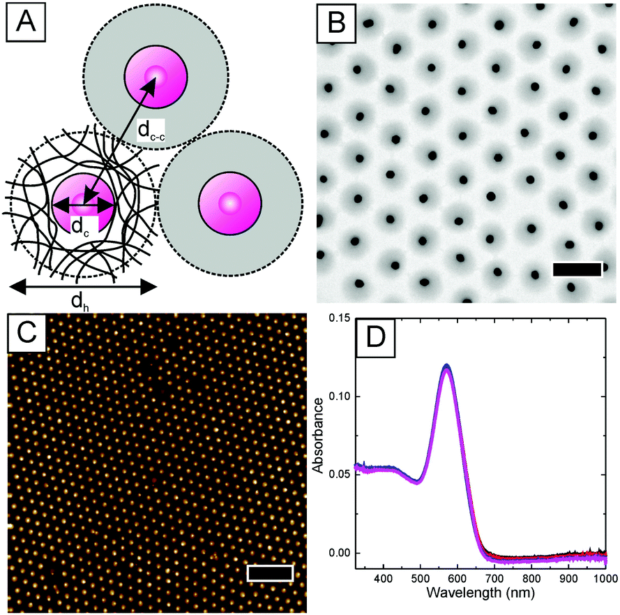 | ||
| Fig. 1 Characterisation of Au@Au–PNIPAM core–shell particles. (A) Schematic illustration of the morphology of the Au@Au–PNIPAM core–shell particles with the hydrodynamic diameter dh, the diameter of the gold cores dc, and the inter-particle center-to-center distance dc–c. (B) Bright-field TEM image of the particles. The scale bar is 500 nm. (C) AFM height profile of a particle monolayer on a glass substrate. The scale bar is 2 μm. (D) UV-Vis absorbance spectra recorded at four random positions of a particle monolayer on a glass substrate. | ||
The core–shell particles (Au–PNIPAM) were prepared by free radical precipitation polymerisation of N-isopropylacrylamide and the cross-linker N,N′-methylenebisacrylamide in the presence of gold nanoparticles in water. This was done following a previously established protocol with gold nanoparticles of 18 nm in diameter surface functionalized with butenylamine.20 The hydrodynamic diameter dh of the resulting core–shell particles was determined to be 330 nm. dh was obtained from dynamic light scattering (DLS) experiments from dilute, aqueous dispersion at 25 °C. Next, the gold cores of the Au–PNIPAM particles were overgrown with gold in situ using a recently published wet-chemical protocol.21 The overgrown particles (Au@Au–PNIPAM) were analysed using transmission electron microscopy (TEM). A representative image of the Au@Au–PNIPAM particles is shown in Fig. 1B. The gold cores and the polymer shell are clearly visible due to the strong difference of electron density between the two materials. An average gold core diameter of 89 nm was obtained from a size distribution histogram of the particles. A narrow polydispersity of 4% was calculated from a Gaussian fit to the particle size distribution. It can be seen that the gold cores are well separated from each other due to the PNIPAM polymer shell.
We have previously shown that the hydrophilic polymer shell surrounding the individual gold nanoparticle cores allows the fabrication of 2D monolayers with defined surface coverage on macroscopic samples (cm-scale) via self-assembly.21 This is an important prerequisite for the implementation of these colloids in solar cells, where structural homogeneity is highly important. Fig. 1C shows an AFM image of a monolayer of the Au@Au–PNIPAM particles prepared on a 2.5 × 2.5 cm2 glass support by transfer from the air/water interface. A detailed description of the coating protocol can be found in the experimental section. The AFM height image reveals a hexagonally ordered, non-close packed monolayer of Au@Au–PNIPAM particles. The empty space between the particles results from shrinkage of the water swollen polymer shell upon drying. AFM measurements of the monolayer in Fig. 1C revealed a maximal vertical distance of 91 ± 5 nm for the Au@Au–PNIPAM particles. Therefore, the separation distance between the plasmonic particles and the substrate is very small which will not affect the near field extension of the gold cores substantially. It is important to note that AFM measurements were performed on multiple points of the glass substrate to investigate the homogeneity of the plasmonic nanostructure. Each time similar results were found. An inter-particle distance of 495 nm was determined from the calculation of the radial distribution function g(r) of the monolayer. Far-field extinction spectra of the particle monolayer were recorded using a UV-Vis spectrometer. Spectra were taken at four random positions of the glass slide and the spectra are displayed in Fig. 1D. The spectra that were recorded at completely independent positions fully overlap emphasising the optical homogeneity of the particle monolayer. The spectra shown in Fig. 1D show a pronounced and narrow peak at 571 nm attributed to the localized surface plasmon resonance (LSPR) of the Au@Au cores. Thus the plasmonic monolayer has a significant extinction in the wavelength range where the photoactive materials are active and it can contribute to the light absorption.
We used our self-assembly strategy to introduce structurally defined plasmonic monolayers to different interfaces of thin-film organic solar cells. An inverted solar cell device architecture with a layer stack of glass/ITO/ZnO/P3HT:PCBM/MoO3/Ag was chosen for the study as it allowed the placement of nanoparticles at different interfaces in a systematic manner. Also more light in-coupling is expected with the ZnO layer due to its higher refractive index than the PEDOT:PSS layer typically employed in the normal device architecture, glass/ITO/PEDOT:PSS/photoactive layer/metal cathode. P3HT:PCBM was selected as a reference photoactive layer, which is the most studied combination in polymer photovoltaic research.25 Additionally, in this photoactive layer a thermal annealing step is usually performed after its deposition to improve the performance. This annealing step is also expected to remove the residual water content resulting from the deposition of the plasmonic core–shell particles. Regioregular P3HT with its stiff backbone is also relatively stable against oxygen/water degradation.26 As shown in Fig. 2, the location of the plasmonic monolayers was systematically and purposefully varied in the inverted solar cell device stack leading to four different types of solar cells. Plasmonic monolayers were incorporated on top of glass/ITO (type 1), glass/ITO/ZnO (type 2 and type 3), and on top of the photoactive layer (type 4). Furthermore in the type 3 solar cell, an additional layer of ZnO was added onto the plasmonic monolayer to completely isolate the gold nanoparticles from the active layer. Thus in type 3, the monolayer was completely embedded in the ZnO dielectric medium. Reference devices without plasmonic monolayers were also prepared and comparatively studied to understand the effect of plasmonic nanoparticles at the different interfaces.
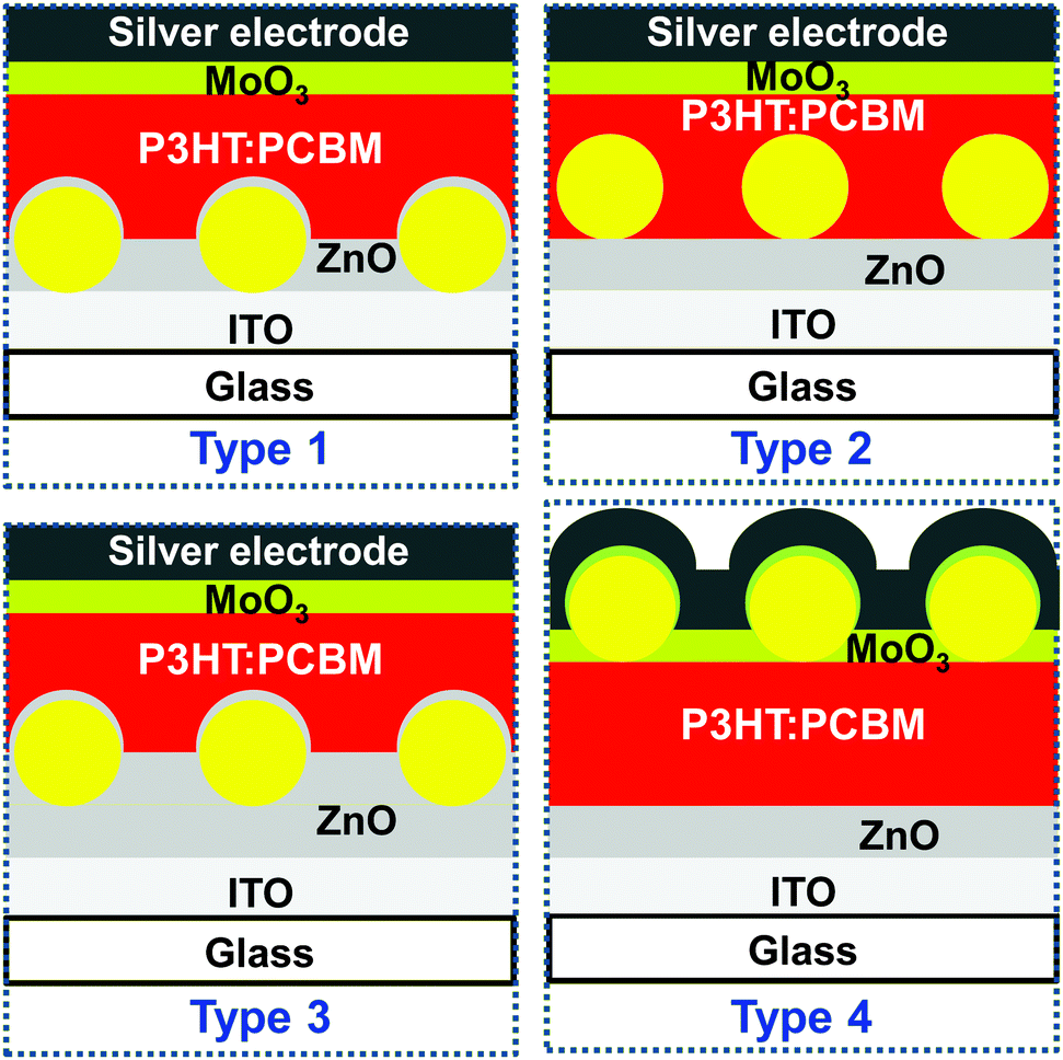 | ||
| Fig. 2 Schematic depictions of the different solar cell architectures used in this work. A monolayer of plasmonic nanoparticles (yellow spheres) was placed on glass/ITO, glass/ITO/ZnO and glass/ITO/ZnO/P3HT:PCBM substrates in type 1, type 2 and type 4 solar cells, respectively. In type 3 solar cells, an additional layer of ZnO was placed on the glass/ITO/ZnO/plasmonic monolayer substrate to isolate the nanoparticles. | ||
To check whether the plasmonic monolayers incorporated at different interfaces (on top of different layers) have comparable morphologies, i.e. order, surface coverage and homogeneity, all monolayers deposited at the different interfaces were investigated using atomic force microscopy (AFM) and cross-sectional scanning electron microscopy (SEM). AFM measurements were performed by scanning on top of the Ag electrode of the fully sandwiched device. In Fig. 3 the results of the AFM and SEM investigation of the type 3 and type 4 solar cells are shown as examples. Fig. 3A displays the AFM height profile of a type 3 solar cell containing a plasmonic monolayer sandwiched within the ZnO interface layer. The AFM image shows slight texturing of the top silver electrode originating from the Au@Au–PNIPAM particles in the ZnO matrix. It is observable that the plasmonic nanostructure in the type 3 device has less topographical contrast compared to the nanostructure, which was prepared on glass (Fig. 1C). This results from the additional layers of ZnO and P3HT:PCBM covering the monolayer and filling the empty space between the particles. In contrast, the plasmonic monolayer shows a strong topographical contrast in the AFM height image of a type 4 solar cell device, where the Au@Au–PNIPAM particles are located at the active layer–MoO3 interface (Fig. 3B).
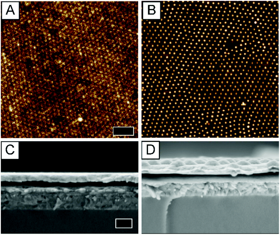 | ||
| Fig. 3 Plasmonic monolayers in type 3 and type 4 solar cell devices. (A and B) AFM investigation of solar cells with plasmonic monolayers located inside the ZnO layer in type 3 (A) and on top of the P3HT:PCBM layer in type 4 (B) respectively. The scale bar corresponds to 2 μm. Both images have the same magnification and are recorded by scanning on top of the Ag electrode. (C and D) Cross-sectional SEM investigation of the same devices shown in (A) and (B). The scale bar corresponds to 200 nm. Both images have the same magnification. | ||
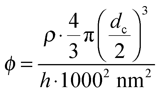
AFM height profiles recorded from all plasmonic solar cells allowed the determination of the center-to-center inter particle distances dc–c, the particle number per unit area ρ as well as the volume fraction ϕ of gold in a virtual layer. ϕ was calculated from ρ by assuming a virtual layer thickness of h = 100 nm determined as the average particle height from the AFM height profiles using the following equation:
 | (1) |
| Sample | d c–c (nm) | ρ (particles per μm2) | ϕ (%) |
|---|---|---|---|
| Glass/Au@Au–PNIPAM | 495 ± 32 | 4.7 | 1.7 |
| Type 1 | 486 ± 45 | 4.7 | 1.7 |
| Type 2 | 461 ± 32 | 5.2 | 1.9 |
| Type 3 | 464 ± 34 | 5.1 | 1.9 |
| Type 4 | 488 ± 153 | 4.8 | 1.8 |
Fig. 3C and D show cross-sectional SEM images of the type 3 and type 4 plasmonic solar cells, respectively. Cross sectional analysis was performed on the same devices as shown in Fig. 3A and B. In Fig. 3C the individual layers of the solar cell device can be distinguished. From bottom to top: glass, ITO, ZnO, the active layer and the silver electrode are clearly visible. The Au@Au–PNIPAM particles are hardly visible in Fig. 3C since the plasmonic particles are completely embedded in ZnO with an upper layer of P3HT:PCBM on top. The top Ag surface also appears to be rather smooth. Thus for the same reason the contrast in the AFM image in Fig. 3A is not as sharp and the SEM surface image shown in Fig. S2A of the ESI† is also featureless. In the case of the type 4 device shown in Fig. 3D, the particles are clearly visible as hemispheres at the interface of P3HT:PCBM and the silver electrode. The hemispheres are a replica of the polymer shell surrounding the gold cores of the Au@Au–PNIPAM particles. In summary, colloidal self-assembly at the air/water interface is a meaningful concept, which allows for the fabrication of defined plasmonic monolayers at any interface of the solar cell device. In the next section, the performance of the plasmonic solar cells will be discussed and the results are analysed in light of optoelectrical investigations.
Solar cell performance
In the literature, the performance of P3HT/PCBM solar cell devices with thin (∼100 nm) films is shown to be limited by weak light absorption.28 On the other hand, the internal quantum efficiency is shown to be as high as 90% for thin P3HT:PCBM solar cell devices.29 Thus in the first series of devices, thin P3HT:PCBM films (118 nm) were used to investigate the potential of plasmonic nanostructures for enhancing light absorption and hence the final solar cell performance. We want to highlight that all types of devices (types 1 to 4) worked independent of the position of the monolayer in the stack and even without the removal of the hydrogel shells surrounding the metal particles.Fig. 4 shows the J–V curves recorded under illumination and in the dark, the external quantum efficiency (EQE) and the total reflectance of the 118 nm thin photoactive layer solar cell devices with plasmonic monolayers at different interfaces. The solar cell performance for each case was checked for reproducibility and consistency by repeating the experiment on different days. Table 2 summarizes the best solar cell performance parameters obtained for each case. The average PCE values obtained from around eight devices are also mentioned in the table. The reference solar cell showed a power conversion efficiency of 2.7%. In general no clear improvement was observed in any of the solar cell types after the incorporation of the nanoparticles. In the type 1 and type 2 solar cell devices, the short circuit currents (Jsc) are lower than for the reference device. The reduced performance i.e. the Jsc and the fill factor (FF) of the type 2 solar cell device can be explained by comparing the dark J–V curves. Fig. 4B shows the dark current on a log-linear scale for all devices, which allows a comparison of the leakage currents (for e.g. J at −1 V) for different types of devices. The high leakage current of the type 2 device where the metal nanoparticles have only the PNIPAM shell and are in direct contact with the active layer explains the reduced performance of the device. Thus in the type 2 device any near-field light absorption enhancement was outweighed by the leakage currents. In order to exclude any leakage current through PNIPAM coated Au particles, a capping layer of ZnO identically processed as the bottom ZnO layer was deposited on top of the plasmonic nanostructure in the type 3 device. Consequently, no extra leakage current could be observed in the type 3 devices. Similarly in the type 4 device, where only a small portion of the metal nanoparticles is in contact with the active layer, no excessive dark leakage currents were observed. Thus type 3 and 4 devices delivered similar short circuit currents compared to the reference devices.
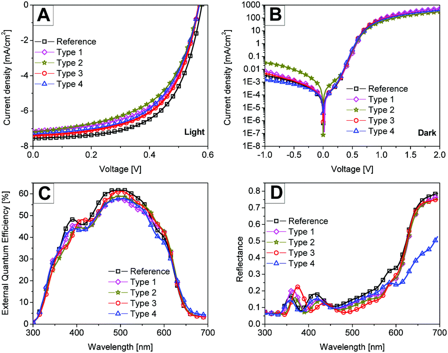 | ||
| Fig. 4 Performance of P3HT:PCBM solar cell devices. (A and B) The current–density–voltage curves under illumination (A) and in the dark (B) for the best solar cell devices. The dark current curves are on a log-linear scale. (C and D) Measured external quantum efficiency (C) and reflectance (D) spectra of the corresponding best solar cell devices. | ||
| Device (thickness) | J sc [mA cm−2] | V oc [V] | FF [%] | PCE [%] |
|---|---|---|---|---|
| Reference [118 nm] | 7.5 (7.5) | 0.59 (0.58) | 61 (58) | 2.7 (2.5) |
| Type 1 [118 nm] | 7.1 (6.7) | 0.58 (0.58) | 58 (57) | 2.4 (2.2) |
| Type 2 [118 nm] | 7.1 (7.0) | 0.58 (0.58) | 55 (54) | 2.3 (2.2) |
| Type 3 [118 nm] | 7.5 (7.3) | 0.58 (0.58) | 58 (54) | 2.5 (2.4) |
| Type 4 [118 nm] | 7.4 (7.5) | 0.58 (0.57) | 56 (56) | 2.4 (2.4) |
| Reference [194 nm] | 5.8 (5.4) | 0.58 (0.58) | 46 (46) | 1.5 (1.4) |
| Type 3 [194 nm] | 5.0 (4.9) | 0.57 (0.58) | 45 (46) | 1.3 (1.3) |
| Type 4 [194 nm] | 7.0 (7.0) | 0.59 (0.58) | 47 (46) | 1.9 (1.9) |
Fig. 4C shows the EQE of the corresponding solar cell devices. The EQE was measured under short circuit conditions under 1000 W m−2 white bias light. The values obtained by convoluting the measured EQE spectra with the AM 1.5 sun spectrum matched well with the Jsc values obtained from IV measurements within the error limits. No clear contribution from plasmonic nanoparticles in photoelectron conversion was observed from the EQE measurements. Fig. 4D shows the total reflectance of the solar cell devices. In general all the plasmonic devices showed a lower reflectance than the reference device in a wavelength range from 400 nm to 630 nm suggesting more light absorption in the device stack. Only the type 4 device with nanostructures at the top of the photoactive layer showed a significantly reduced reflectance for wavelengths greater than 630 nm. In this region the P3HT:PCBM photoactive layer or any other layer in the device stack, except for the Ag electrode, does not absorb light efficiently. Since we did not see any enhancement in the EQE spectra, we conclude that the observed extra light absorption with the nanostructures is lost as parasitic absorption.
In order to elucidate this effect more clearly, the transmission spectra of a type 3 solar cell substrate ITO/ZnO/NPs/ZnO and the reference substrate without any nanoparticles (NPs) are compared in Fig. 5. The transmission of the type 3 substrate is significantly lower as compared to the reference device substrate for wavelengths larger than 370 nm. In addition the transmission of the plasmonic device shows a pronounced dip between 550 and 650 nm which can be attributed to the LSPR of the plasmonic particles. Compared to the LSPR measured from a plasmonic monolayer on glass (see Fig. 1D), the LSPR in the device is redshifted by around 40 nm. This shift is related to the higher refractive environment of the monolayer in the ZnO matrix in the type 3 device as compared to the monolayer at the glass/air interface.30 Thus comparing Fig. 4D and 5 it can be concluded that the parasitic absorption mainly originates from the plasmonic monolayer. Instead of improving the performance of solar cells by contributing to the charge transfer or energy transfer,31 the plasmonic layer in this architecture reduces the solar cell performance.
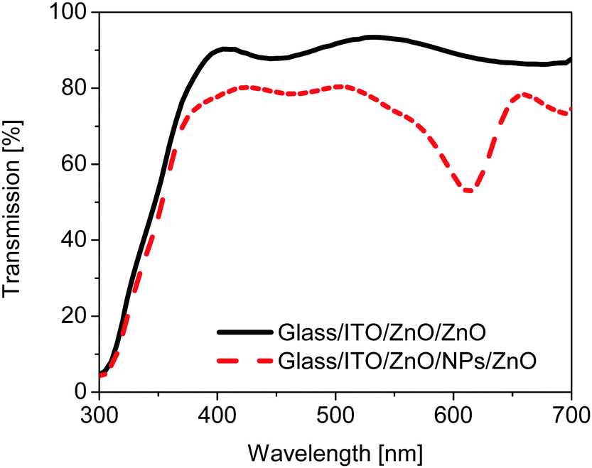 | ||
| Fig. 5 Comparison of the transmission spectra of glass/ITO/ZnO/ZnO substrates with (dash) and without (line) a monolayer of nanoparticles within the ZnO layer. | ||
In order to better understand the role of plasmonic particles, solar cell devices with thick active layers were also investigated. In such a device, the charge transport and not the light absorption would be the limiting factor and hence parasitic absorption might now completely mask the positive contribution of the plasmonic particles. Thick active layers are also technologically relevant as they are easier to realize via roll-to-roll processing and less prone to defects.32 Thus solar cells were fabricated using a thick layer of P3HT:PCBM (194 nm) and the performance of the reference device was compared with the type 3 and type 4 based devices. Only types 3 and 4 were selected for this case due to the minimum leakage current in these structures. Fig. 6A shows the J–V curves under AM 1.5 sun illumination and in the dark of the thick devices with and without the nanostructure. Table 2 also summarizes the best solar cell performance parameters obtained for each case of the thick active layer device. As expected, in the thick active layer devices, where the light absorption mostly occurs in the photoactive layer near the bottom ZnO interface, the performance of all devices was lower compared to the optimized thin active layer based devices.
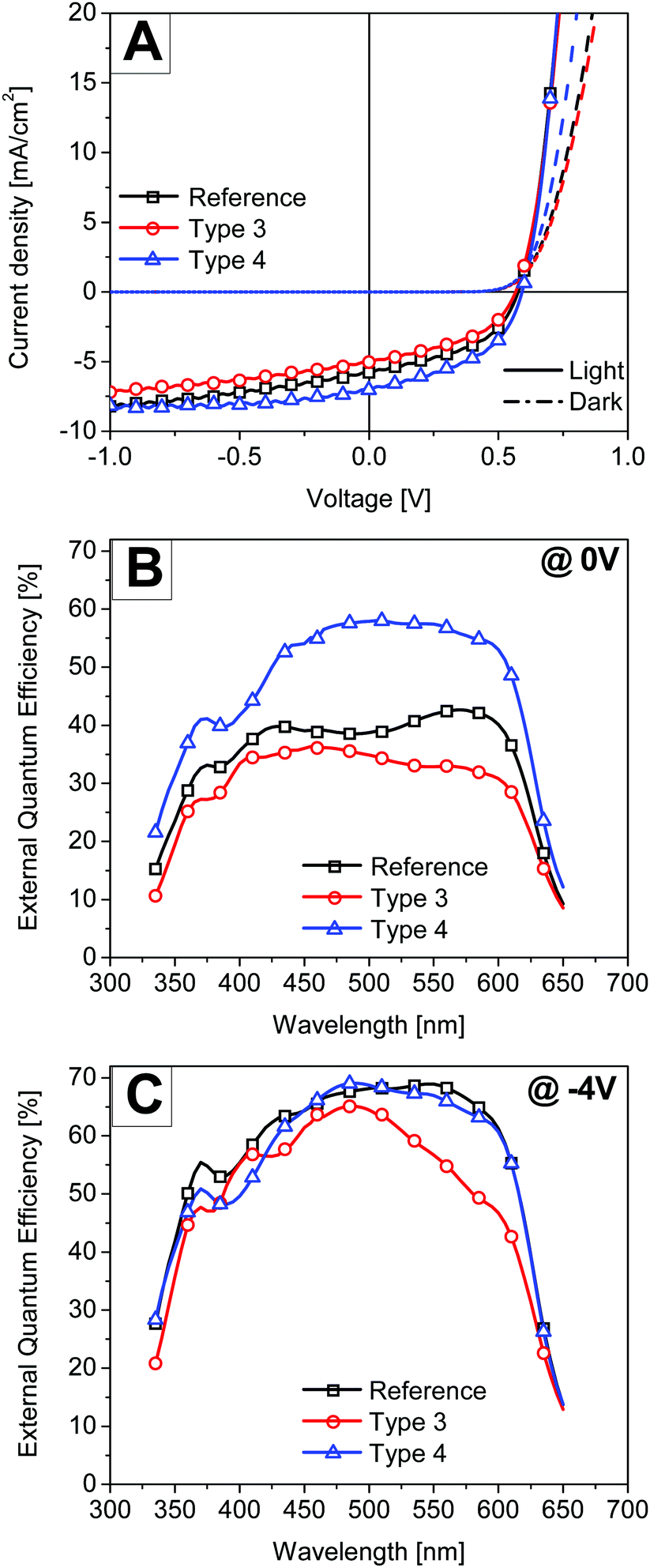 | ||
| Fig. 6 Performance of thick P3HT:PCBM active layer solar cell devices. (A) The current–density–voltage curves under illumination and in the dark for the best solar cell devices. (B and C) Measured external quantum efficiency spectra of the corresponding solar cell devices under a white bias light of 800 W m−2 at 0 V (B) and −4 V (C) applied voltage. | ||
The power conversion efficiency of the thick active layer reference device was 1.5%. In the literature, this reduced performance is attributed to excessive bulk recombination as the lower mobility hole carriers need to travel a larger distance to the top electrode.33 For very thick active layer films, slow moving charge carriers might also accumulate inside the active layer leading to a space charge limited photocurrent. In contrast to the results of the thin active layer solar cells, the performance of the thick type 4 solar cell was clearly better than the reference device. The performance of the type 3 solar cell was again lower than that of the reference device. Fig. 6B shows the EQE of all the respective thick devices measured under a white bias light of 800 W m−2 under short circuit conditions. The white bias light was applied to nearly match the conditions under which the I–V scans were performed. It is clear from the asymmetric EQE spectrum of the reference device that the excitons created by the deep penetration of light in the active layer at wavelengths 425 nm and 600 nm contribute better to the photoelectron conversion than the ones from the 500 nm light where the P3HT:PCBM film has the most absorption. Surprisingly the type 4 solar cell device showed the perfect square shape EQE spectrum suggesting uniform charge collection at all wavelengths. Since the active layer was identical and the hole transport will equally be critical for all the cases, the observed high EQE values in the type 4 solar cell suggest that significant charge generation occurs next to the top electrode. This charge generation will lead to an efficient hole collection at the anode. Sha et al. also demonstrated that the space charge limit in thick P3HT:PCBM inverted solar cells can be prevented by employing a metal grating anode.34 The metal grating electrode was prepared using the polydimethylsiloxane (PDMS) nanoimprinting method onto the surface of the active layer. However here a simple approach is presented where the interface assisted self-assembly of a monolayer of metal particles can be used at the top interfaces to prevent the build-up of space charge and extract slow moving charge carriers efficiently.
EQE was also measured at −4 V bias voltage to separate optical losses from electronic losses. At high reverse bias voltages, all photo-generated charges are “forcefully” collected and the solar cell performance is only limited by the amount of light absorption in the active layer. Fig. 6C shows the EQE of all the respective devices measured under white bias light of 800 W m−2 at −4 V bias voltage. By comparing the EQE spectra of the type 3 device with the reference, it is clear that the main optical loss mechanism in the type 3 solar cells is due to parasitic absorption in the nanostructure in a wavelength range from 500 nm to 600 nm. The figure also shows that the EQE spectrum of the type 4 device matches well with that of the reference device in a wavelength region 450 nm to 650 nm except for a small drop in quantum efficiency at around 600 nm which we assign to plasmonic absorption. Thus by comparing the EQE spectra at −4 V it can be concluded that there is no additional light absorption in the active layer of the type 4 solar cell. Sha et al. also suggested that metallic nanostructures can be used to tune the electrical properties of solar cells via the plasmon-modified optical field distribution.15 In that study the total optical absorption of plasmonic solar cells was independent of the nanoparticle positions in the active layer and only the light redistributed spatially by localized plasmonic effects. Thus it is clear from our study that the plasmonic monolayer near the electrode spatially redistributes the light and charge generation close to the electrode leading to an improved performance. But at present it is difficult to distinguish between the contribution of near-field enhancement and light-scattering effects in the light absorption process near the top electrode.
In summary only the type 4 solar cell geometry when used with thick active layers showed a clear improvement in performance compared to the reference devices. We also understand that there have been reports where an improvement in performance is demonstrated by placing randomly distributed gold particles of a broad range of sizes ranging from 15 to 70 nm underneath the active layer.4,11,12,35 The Au-particle size in the present study is 89 nm. But still there is no consensus about the optimum size of the particles and it is unclear whether the observed effects arise from the particle size or other effects such as the particle density, or the inter-particle distance. In this case, the presented colloidal self-assembly approach allows a way to solve the above-mentioned discrepancies by further studying the influence of particle diameter and NP–NP distance in a systematic way. Our observation that there is an improvement only in the type 4 solar cell geometry also finds support in inorganic thin film Si-based solar cells, where it has been well established that metal nanoparticles should be located at the rear of the cells in a plasmonic back reflector (PRB) configuration to harness the light scattering effects.36 Mendes et al. also showed a considerable improvement in thin film n–i–p nanocrystalline silicon solar cells using colloidal nanoparticles in the PRB configuration.37
Conclusions
The self-assembly of metal–polymer core–shell particles at the air/water interface is introduced as a colloidal self-assembly concept for the fabrication of optically homogenous monolayers of plasmonic nanoparticles. In order to address the optoelectrical effects of plasmonic nanoparticles in organic solar cells, plasmonic monolayers were successfully introduced at different interfaces of P3HT:PCBM based inverted organic solar cells. The plasmonic layers showed a hexagonal arrangement of well-separated nanoparticles with an average inter-particle distance of 480 nm independent of the monolayer position in the devices. Despite the polymer shell around the nanoparticles, the direct contact of particles with the active layer led to excessive leakage currents and consequently the performance was reduced. Incorporating the nanostructure at any bottom interface underneath the active layer did not lead to improved performance due to parasitic absorption arising from the LSPR of the plasmonic particles. We could not find evidence for direct charge transfer or energy transfer contributions to the EQE of the device from plasmonic absorption in thin devices. In thick active layer solar cells where the charge transport is limited by the low hole mobility of charge carriers, the plasmonic nanostructure at the top of the active layer spatially redistributed the light absorption and charge generation close to the top hole extracting electrode led to an improved performance. Thus the application of particles on top of appreciably thick photoactive layer devices is a more promising approach to harness the near-field effects and it can also provide the benefit of light trapping at longer wavelengths without the problem of parasitic absorption. In general, this work clearly highlights that the incorporation of metal nanoparticles is not a straightforward remedy to improve the absorption and hence performance of organic solar cells. All factors including exciton quenching, dark leakage currents and parasitic absorption need to be meticulously considered for solar cell design.Acknowledgements
We gratefully acknowledge the financial support from the German Science Foundation DFG (SFB 840), the Bavarian State Ministry for Environment and Consumer Protection (UMWELTnanoTECH) and the Bavarian State Ministry of Science, Research, and the Arts through the Collaborative Research Network “Solar Technologies go Hybrid”.References
- (a) Y. Liu, J. Zhao, Z. Li, C. Mu, W. Ma, H. Hu, K. Jiang, H. Lin, H. Ade and H. Yan, Nat. Commun., 2014, 5, 5293 CrossRef CAS PubMed; (b) Z. He, B. Xiao, F. Liu, H. Wu, Y. Yang, S. Xiao, C. Wang, T. P. Russell and Y. Cao, Nat. Photonics, 2015, 9, 174–179 CrossRef CAS; (c) L. Lu, T. Zheng, Q. Wu, A. M. Schneider, D. Zhao and L. Yu, Chem. Rev., 2015, 115, 12666–12731 CrossRef CAS PubMed.
- M. Karg, T. A. König, M. Retsch, C. Stelling, P. M. Reichstein, T. Honold, M. Thelakkat and A. Fery, Mater. Today, 2015, 18, 185–205 CrossRef CAS.
- H. A. Atwater and A. Polman, Nat. Mater., 2010, 9, 205–213 CrossRef CAS PubMed.
- H. L. Gao, X. W. Zhang, Z. G. Yin, H. R. Tan, S. G. Zhang, J. H. Meng and X. Liu, Appl. Phys. Lett., 2012, 101, 133903 CrossRef.
- H. Choi, J.-P. Lee, S.-J. Ko, J.-W. Jung, H. Park, S. Yoo, O. Park, J.-R. Jeong, S. Park and J. Y. Kim, Nano Lett., 2013, 13, 2204–2208 CrossRef CAS PubMed.
- S. Li, W. Li, Q. Liu, H. Wei, E. Jin, H. Wang, Y. Dong, H. Lu, X. Zhang, X. Zhao, M. Wang and Z. Bo, J. Mater. Chem. C, 2015, 3, 1319–1324 RSC.
- X. Li, X. Ren, F. Xie, Y. Zhang, T. Xu, B. Wei and W. C. H. Choy, Adv. Opt. Mater., 2015, 3, 1220–1231 CrossRef CAS.
- Y.-M. Sung, Y.-C. Lai, M.-F. Tsai, H.-H. Hsieh, M.-H. Yang, P. P. Wei, C.-S. Yeh, F.-C. Hsu and Y.-F. Chen, J. Mater. Chem. C, 2016, 4, 513–520 RSC.
- (a) S.-W. Baek, J. Noh, C.-H. Lee, B. Kim, M.-K. Seo and J.-Y. Lee, Sci. Rep., 2013, 3 Search PubMed; (b) T. Kawawaki, Y. Takahashi and T. Tatsuma, J. Phys. Chem. C, 2013, 117, 5901–5907 CrossRef CAS.
- F. Pastorelli, S. Bidault, J. Martorell and N. Bonod, Adv. Opt. Mater., 2014, 2, 171–175 CrossRef.
- L. Lu, Z. Luo, T. Xu and L. Yu, Nano Lett., 2013, 13, 59–64 CrossRef CAS PubMed.
- J. Wang, Y.-J. Lee, A. S. Chadha, J. Yi, M. L. Jespersen, J. J. Kelley, H. M. Nguyen, M. Nimmo, A. V. Malko, R. A. Vaia, W. Zhou and J. W. P. Hsu, J. Phys. Chem. C, 2013, 117, 85–91 CAS.
- (a) D. U. Karatay, M. Salvador, K. Yao, A. K.-Y. Jen and D. S. Ginger, Appl. Phys. Lett., 2014, 105, 33304 CrossRef; (b) R. B. Dunbar, T. Pfadler and L. Schmidt-Mende, Opt. Express, 2012, 20, A177 CrossRef CAS PubMed.
- (a) S. Pillai and M. A. Green, Sol. Energy Mater. Sol. Cells, 2010, 94, 1481–1486 CrossRef CAS; (b) T. Pfadler, M. Stärk, E. Zimmermann, M. Putnik, J. Boneberg, J. Weickert and L. Schmidt-Mende, APL Mater., 2015, 3, 66101 CrossRef.
- W. E. I. Sha, H. L. Zhu, L. Chen, W. C. Chew and W. C. H. Choy, Sci. Rep., 2015, 5, 8525 CrossRef CAS PubMed.
- (a) S. H. Ahn, D. J. Kim, W. S. Chi and J. H. Kim, J. Mater. Chem. A, 2015, 3, 10439–10447 RSC; (b) Y. H. Jang, Y. J. Jang, S. T. Kochuveedu, M. Byun, Z. Lin and D. H. Kim, Nanoscale, 2014, 6, 1823–1832 RSC.
- (a) D. H. Wang, D. Y. Kim, K. W. Choi, J. H. Seo, S. H. Im, J. H. Park, O. O. Park and A. J. Heeger, Angew. Chem., Int. Ed., 2011, 50, 5519–5523 CrossRef CAS PubMed; (b) S. Liu, R. Jiang, P. You, X. Zhu, J. Wang and F. Yan, Energy Environ. Sci., 2016, 9, 898–905 RSC; (c) S. Liu, R. Jiang, P. You, X. Zhu, J. Wang and F. Yan, Energy Environ. Sci., 2016, 9, 898–905 RSC.
- (a) M. Saliba, W. Zhang, V. M. Burlakov, S. D. Stranks, Y. Sun, J. M. Ball, M. B. Johnston, A. Goriely, U. Wiesner and H. J. Snaith, Adv. Funct. Mater., 2015, 25, 5038–5046 CrossRef CAS; (b) Z. Lu, X. Pan, Y. Ma, Y. Li, L. Zheng, D. Zhang, Q. Xu, Z. Chen, S. Wang, B. Qu, F. Liu, Y. Huang, L. Xiao and Q. Gong, RSC Adv., 2015, 5, 11175–11179 RSC.
- N. Vogel, M. Retsch, C.-A. Fustin, A. del Campo and U. Jonas, Chem. Rev., 2015, 115, 6265–6311 CrossRef CAS PubMed.
- M. Karg, S. Jaber, T. Hellweg and P. Mulvaney, Langmuir, 2011, 27, 820–827 CrossRef CAS PubMed.
- T. Honold, K. Volk, A. Rauh, J. P. S. Fitzgerald and M. Karg, J. Mater. Chem. C, 2015, 3, 11449–11457 RSC.
- B. Ebeling and P. Vana, Macromolecules, 2013, 46, 4862–4871 CrossRef CAS.
- C. R. Singh, C. Li, C. J. Mueller, S. Hüttner and M. Thelakkat, Adv. Mater. Interfaces, 2016, 3, 1500422 CrossRef.
- N. Vogel, S. Goerres, K. Landfester and C. K. Weiss, Macromol. Chem. Phys., 2011, 212, 1719–1734 CrossRef CAS.
- M. T. Dang, L. Hirsch and G. Wantz, Adv. Mater., 2011, 23, 3597–3602 CrossRef CAS PubMed.
- W. R. Mateker, T. Heumueller, R. Cheacharoen, I. T. Sachs-Quintana, M. D. McGehee, J. Warnan, P. M. Beaujuge, X. Liu and G. C. Bazan, Chem. Mater., 2015, 27, 6345–6353 CrossRef CAS.
- K. Volk, J. P. S. Fitzgerald, M. Retsch and M. Karg, Adv. Mater., 2015, 27, 7332–7337 CrossRef CAS PubMed.
- H. Hoppe, S. Shokhovets and G. Gobsch, Phys. Status Solidi RRL, 2007, 1, R40–R42 CrossRef CAS.
- B. Liu, R.-Q. Png, L.-H. Zhao, L.-L. Chua, R. H. Friend and P. K. Ho, Nat. Commun., 2012, 3, 1321 CrossRef PubMed.
- D. D. Evanoff, R. L. White and G. Chumanov, J. Phys. Chem. B, 2004, 108, 1522–1524 CrossRef CAS.
- K. O. Aruda, M. Tagliazucchi, C. M. Sweeney, D. C. Hannah and E. A. Weiss, Phys. Chem. Chem. Phys., 2013, 15, 7441 RSC.
- J. Alstrup, M. Jørgensen, A. J. Medford and F. C. Krebs, ACS Appl. Mater. Interfaces, 2010, 2, 2819–2827 CAS.
- T. J K Brenner, Y. Vaynzof, Z. Li, D. Kabra, R. H. Friend and C. R. McNeill, J. Phys. D: Appl. Phys., 2012, 45, 415101 CrossRef.
- W. E. I. Sha, X. Li and W. C. H. Choy, Sci. Rep., 2014, 4, 6236 CrossRef CAS PubMed.
- (a) J.-L. Wu, F.-C. Chen, Y.-S. Hsiao, F.-C. Chien, P. Chen, C.-H. Kuo, M. H. Huang and C.-S. Hsu, ACS Nano, 2011, 5, 959–967 CrossRef CAS PubMed; (b) D. Chi, S. Lu, R. Xu, K. Liu, D. Cao, L. Wen, Y. Mi, Z. Wang, Y. Lei, S. Qu and Z. Wang, Nanoscale, 2015, 7, 15251–15257 RSC.
- (a) H. Tan, R. Santbergen, A. H. M. Smets and M. Zeman, Nano Lett., 2012, 12, 4070–4076 CrossRef CAS PubMed; (b) S. Morawiec, M. J. Mendes, S. A. Filonovich, T. Mateus, S. Mirabella, H. Aguas, I. Ferreira, F. Simone, E. Fortunato, R. Martins, F. Priolo and I. Crupi, Opt. Express, 2014, 22, A1059–A1070 CrossRef PubMed.
- M. J. Mendes, S. Morawiec, T. Mateus, A. Lyubchyk, H. Aguas, I. Ferreira, E. Fortunato, R. Martins, F. Priolo and I. Crupi, Nanotechnology, 2015, 26, 135202 CrossRef PubMed.
Footnotes |
| † Electronic supplementary information (ESI) available. See DOI: 10.1039/c6cp04451d |
| ‡ C. R. S. and T. H. contributed equally to this work. |
| § Present address: Institute of Physical Chemistry and Polymer Physics, Leibniz Institute of Polymer Research Dresden, 01005 Dresden, Germany. |
| ¶ Present address: Department of Physical Chemistry 1, Heinrich Heine-University Duesseldorf, 40225 Duesseldorf, Germany. |
| This journal is © the Owner Societies 2016 |