
 Open Access Article
 This Open Access Article is licensed under a
 Creative Commons Attribution 3.0 Unported Licence
Decoupling the effects of confinement and passivation on semiconductor quantum dots
Roya
Rudd
a,
Colin
Hall
a,
Peter J.
Murphy
a,
Peter J.
Reece
b,
Eric
Charrault
a and
Drew
Evans
 *a
*a
aFuture Industries Institute, University of South Australia, Mawson Lakes, South Australia, 5095, Australia. E-mail: roya.rudd@mymail.unisa.edu.eu; colin.hall@unisa.edu.au; Peter.J.Murphy@unisa.edu.au; Eric.Charrault@unisa.edu.au; Drew.Evans@unisa.edu.au; Fax: +61 8 8302 3683; Tel: +61 8 83025719
bSchool of Physics, University of New South Wales, Sydney, NSW 2052, Australia. E-mail: p.reece@unsw.edu.au
First published on 5th July 2016
Abstract
Semiconductor (SC) quantum dots (QDs) have recently been fabricated by both chemical and plasma techniques for specific absorption and emission of light. Their optical properties are governed by the size of the QD and the chemistry of any passivation at their surface. Here, we decouple the effects of confinement and passivation by utilising DC magnetron sputtering to fabricate SC QDs in a perfluorinated polyether oil. Very high band gaps are observed for fluorinated QDs with increasing levels of quantum confinement (from 4.2 to 4.6 eV for Si, and 2.5 to 3 eV for Ge), with a shift down to 3.4 eV for Si when oxygen is introduced to the passivation layer. In contrast, the fluorinated Si QDs display a constant UV photoluminescence (3.8 eV) irrespective of size. This ability to tune the size and passivation independently opens a new opportunity to extending the use of simple semiconductor QDs.
Introduction
With the breakthroughs over the past decades in Semiconductor (SC) materials and processing, SCs have been critical to rapid development of today's modern electronic and optoelectronic devices. Silicon (Si) and to a lesser extent germanium (Ge) are two examples of materials central to this technological development. On a fundamental level, both these are classed as indirect band gap SCs and therefore are not considered as efficient emitters of high energy light.1,2 High energy emission (short wavelength) allows for sharper focus of the light and operation without production of waste heat radiation (unlike infrared light). UV light emitters are therefore of interest in different applications such as compact UV sources, light emitting diodes, biomedical and photodetectors.3–6The discovery of photoluminescence (PL) from porous Si at wavelengths corresponding to red light in the early 1990s changed the understanding of the emission mechanism of Si, opening the possibilities for new optoelectronic applications.7 In the first instance, the PL in porous Si is interpreted as arising from quantum confinement effects which results in an increase (blue shift) of the optical absorption energy (band gap).8,9 In the nanometre size range, quantum confinement appears to play a fundamental role in effecting the electronic structure and optical behaviour of semiconductor quantum dots (QDs).10 The energy gap between the highest occupied molecular orbital (HOMO) and lowest unoccupied molecular orbital (LUMO) increases as a result of quantum confinement.11 Although theoretical calculations and some experimental results support this interpretation,9,12–15 it has been challenged by observations that surface passivation also plays a role.16–18 Isolated Si QDs in the gas phase do not reveal any visible emission after UV excitation19 with theoretically zero or close to zero calculated band gap for unpassivated Si QDs.20 Dangling bonds cause recombination of electrons and holes without emission of light for unpassivated QDs. Conversely, the band gap for passivated QDs (no dangling bonds) is reported to be on the order of several eV.21 The same argument can be presented for any SC material, with reports confirming these observations for Ge.22
In SC QDs, owing to the very high surface area to volume ratio, most of the atoms are positioned at or near the surface. Owing to their location at the surface, they are affected by any surface effects or passivation. In turn this yields a substantial modification of the QDs electronic structures and optical properties.23,24 It was reported in the early 1990's that H passivation of Si QDs was critical for luminescence.25 Later studies observed that O passivation (especially Si![[double bond, length as m-dash]](https://www.rsc.org/images/entities/char_e001.gif) O bonds) significantly reduced the optical band gap and visible light emission relative to H passivation for particles below 1.5 nm.26,27 In recent years it has emerged through both experiment28–30 and theory24 that the dielectric matrix surrounding the QD plays a decisive role in determining its optical properties. From the results of the bare and passivated Si QDs, it can be concluded that surface passivation in addition to quantum confinement determine the optical behaviour of Si QDs.16,31,32 Therefore, one remaining challenge is to clearly separate the effects of quantum confinement and interfacial chemistry in experimental studies.24,33,34 This interplay between quantum confinement and interfacial chemistry on the optical properties of SC QDs is partly due to limitations in the QDs fabrication processes. Moving beyond Si, Little et al. recently highlighted that the photoluminescence of Ge QDs was attributed to passivation of their surface, typically arising during the fabrication process itself.22
O bonds) significantly reduced the optical band gap and visible light emission relative to H passivation for particles below 1.5 nm.26,27 In recent years it has emerged through both experiment28–30 and theory24 that the dielectric matrix surrounding the QD plays a decisive role in determining its optical properties. From the results of the bare and passivated Si QDs, it can be concluded that surface passivation in addition to quantum confinement determine the optical behaviour of Si QDs.16,31,32 Therefore, one remaining challenge is to clearly separate the effects of quantum confinement and interfacial chemistry in experimental studies.24,33,34 This interplay between quantum confinement and interfacial chemistry on the optical properties of SC QDs is partly due to limitations in the QDs fabrication processes. Moving beyond Si, Little et al. recently highlighted that the photoluminescence of Ge QDs was attributed to passivation of their surface, typically arising during the fabrication process itself.22
Examination of literature reveals that several techniques exist to fabricate SC QDs. By far the most popular is the chemical pathway, where the SC cation of a salt is chemically reduced to precipitate out the SC QDs. The challenges facing this pathway are the (i) possible halide (anion of the salt) impurities trapped within the QD, and (ii) fixed passivation due to the ligand stabilisers used in solution.35 Conversely, chemical vapour deposition using plasma processes has been successfully utilised to fabricate pristine SC QDs.35–38 A feed gas of a SC analogue to methane (i.e. SiH4 or GeH4) is fragmented in the plasma, which recondense into SC QDs. Passivation is achieved by introducing select gases to the plasma, such as H2. The limitation arises for both these techniques that the act of changing passivation concurrently leads to a change in QD size, and typically to change the QD size requires a change in the passivation chemistry. This motivates the need to independently investigate the effect of confinement and passivation on the optical properties of SC QDs, as control of a QD's optical properties has practical importance for device fabrication.
Herein, we present DC magnetron sputtering of SC materials into a negligible vapour pressure liquid. The sputtering process allows control of the QD size approaching 1 nm without the requirement for chemical precursors or stabilising agents/capping ligand molecules.39–44 Alternatively the choice of liquid and presence of low partial pressure gases (O2) in the sputter chamber gives control of the surface passivation. As a result, very small QDs are fabricated and readily passivated in the liquid to yield SC QDs with very high band gap. For Si, PL energies are in the UV region. Perfluorinated Polyether (PFPE) was selected as the dielectric matrix into which both Si and Ge QDs were deposited. This optically transparent fluoropolymer has negligible vapour pressure and is chemically inert while containing many fluorine atoms. Furthermore, PFPE does not emit light when excited with high-photon energy; in fact it has been reported as a PL quencher.45 The presence of fluorine atoms in principal leads to significant impact on the optical properties of SC QDs owing to their large electronegativity and small size; without making any direct bonds with the SC QDs.
Experimental section
Sputter deposition
Fabrication of SC QDs was performed by magnetron sputtering from a 5′′ × 12′′ rectangular Si target (99.99% in purity) or a 3′′ circular Ge target (99.99% in purity). 2 ml (∼1 mm thick) of PFPE (Solvay Solexis, Mw: 1800 g mol−1) which was dried under vacuum for 24 h was spread on a glass plate (24 cm2) that was horizontally set in the sputtering chamber at a distance of 10.5 cm from the target. Sputtering was conducted under a constant Ar flow rate of 60 sccm and pressure of 2.9 × 10⁻³ mbar. Sputtering conditions and rates are given in Table 1. Before the deposition, the target was presputtered, to remove any possible oxide layer and surface contamination, and after sputtering the samples were stored in a desiccator to keep them dry.| Sample | Power [W] | Deposition time [min] | Deposition rate [nm s−1] | |
|---|---|---|---|---|
| Si | A | 500 | 5 | 0.31 |
| B | 500 | 20 | 0.37 | |
| C | 500 | 45 | 0.39 | |
| D | 800 | 20 | 0.44 | |
| E | 1100 | 20 | 0.71 | |
| Ge | F | 60 | 20 | 0.74 |
| G | 80 | 20 | 0.78 | |
| H | 100 | 20 | 0.81 | |
To change the surface chemistry of the ejected SC QDs, a low flow rate of 5 sccm O2 was introduced into the sputtering chamber during deposition for both Si and Ge (under similar conditions to samples B and G, respectively). The pressure during sputtering was 2.97 × 10⁻³ mbar. The voltage of the Si (Ge) target was kept constant indicating that metallic sputtering mode was still in effect (the target surface was not poisoned by the O2). Increasing the O2 flow rate more than 5 sccm was not possible due to poisoning of the target and the subsequent sputtering of SiO2 (GeO2).
Sample characterization
UV-vis absorption spectra were recorded between 200 and 800 nm at room temperature on a Cary Varian 5000 spectrophotometer. For the spectroscopic measurements, the PFPE containing the SC QDs was poured into a Helma quartz cuvette with an optical path length of 10 mm. The absorption of PFPE was recorded under the same beam conditions.For PL measurements of the Si QDs the excitation sources was the Third-Harmonic-Generation (THG) of a mode-locked Ti:Sapphire laser operating at 1.65 eV (i.e. excitation was done at 4.95 eV). The pulse duration of the excitation source was about 200 fs and the average power was approximately 30 mW. A thermoelectric cooled photomultiplier tube (TE-cooled PMT) and lock-in amplifier mounted to a 50 cm focal length spectrometer were used. All measurements were done under ambient conditions in a 10 mm quartz cuvette (Starna).
Transmission electron microscopy (TEM) images were taken on a Philips CM 200 FEG apparatus operating at an acceleration voltage of 200 kV. The QDs were studied by TEM directly in the PFPE. The TEM samples were prepared by putting a drop of solution on a copper grid (200 mesh) covered with a lacey carbon film (Proscitech, Australia) and draining the excess of PFPE.
Results and discussion
In the sputtering process the bombardment of a target with an ionised working gas (typically inert gas such as Ar, leading to Ar+) causes the physical ejection of surface atoms and/or clusters (Fig. 1). In the context of this study, we define the ejected clusters as the QDs. The use of liquid substrates has been reported in place of conventional solid substrates for collecting and stabilizing metal nanoparticles during sputter deposition.39–44 However the role of PFPE in this study is not only as the capture medium (due to its low vapour pressure and being chemically inert) for collecting and stabilizing SC QDs, in fact PFPE which contains many F atoms was selected as the dielectric matrix. We show that using the PFPE as the matrix improves the optical properties of resultant SC QDs.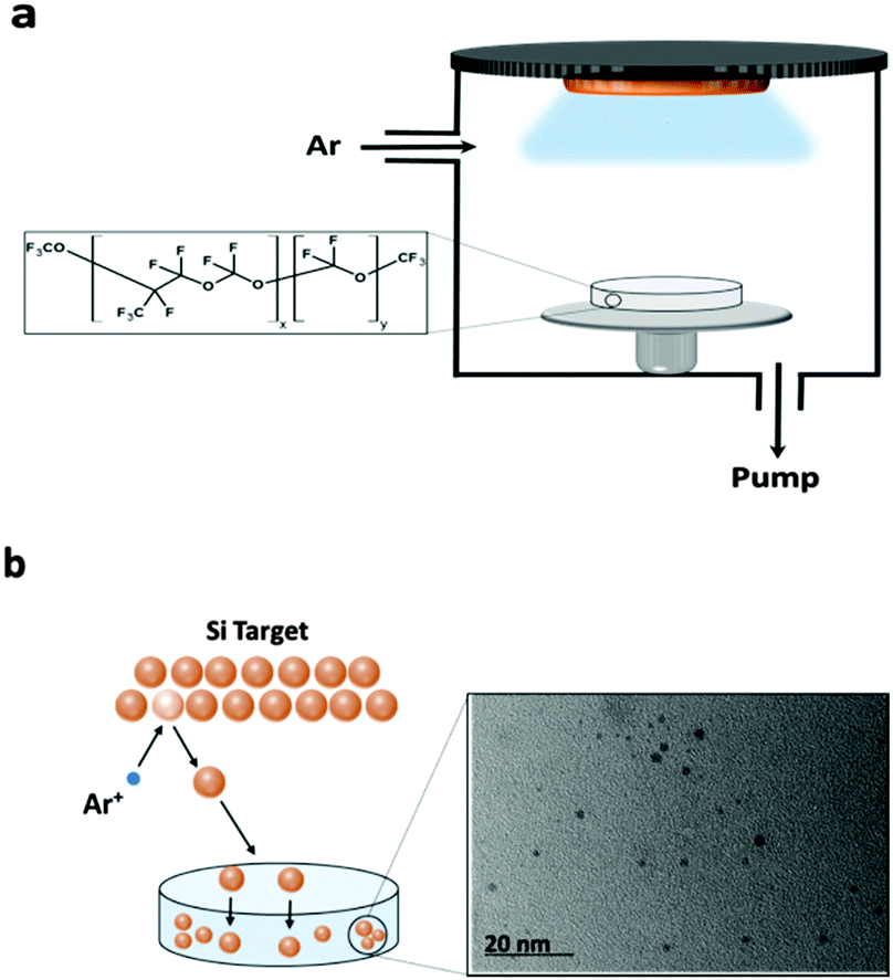 | ||
| Fig. 1 (a) Representative scheme of a typical DC-magnetron sputtering system. (b) Details of the process: ejection of Si atoms by ionised Ar into a reservoir of PFPE, and a typical TEM image of sputtered Si QDs in PFPE. | ||
In order to confirm the presence of SC QDs, UV-vis and TEM were used. A typical TEM image of sputtered Si QDs into the PFPE is shown in Fig. 1b. The power applied to the Si sputter target (2400 W) for the sample shown in Fig. 1b is much higher than those of other samples in this study, hence the relatively larger particle size of approximately 3–5 nm. These larger particles are more easily detectable using TEM. The detection of Si QDs in the other samples with lower sputtering power was attempted, however the low concentration of the Si QDs and their Brownian motion in the PFPE made TEM imaging challenging.
Due to the low gas pressure there are no considerable gas-phase collisions of the sputtered species in the space between the target and the PFPE medium, so condensation of the QDs into aggregates are unlikely. After traversing the vacuum, the QDs deposit into the PFPE to produce a SC QD dispersion. Observation shows that a continuous film does not form at the vacuum/liquid surface, which suggests penetration of the atoms/clusters into the PFPE. Other mechanisms proposed for the sputter synthesis of (metal) QDs in ionic liquids involve injection of very small sputtered clusters, with subsequent coalescence into a QD occurring on the surface or within the liquid. This mechanism has been proposed because different ionic liquids have been shown to create different sized QDs.39,46 We propose that due to the smaller size of the sputtered SC QDs compared to the PFPE molecules, the ejected atoms/clusters penetrate the surface of the PFPE without experiencing any nucleation and are stabilized by the PFPE molecules, which completely cover each SC QD. In addition, because the PFPE molecules carry no charge and their stabilization process is not electrostatic repulsion similar to ionic liquid, if the growth happened within the PFPE, the particles should disorder the orientation of the medium and in high concentrations this would lead to phase separation for larger particles.
In Fig. 2 the UV-vis absorption spectra of sputtered Si and Ge QDs in PFPE are shown. A clear absorption edge corresponding to the optical band gap can be found for all of the samples. The absorption spectra indicate that the particles’ absorptions are in the UV region. In general, the intensity of the absorption of samples sputtered for 5, 20 and 45 min with 500 W increases with the sputtering time (Fig. 2a) which can be attributed to the different concentrations of Si QDs in the PFPE. Fig. 2b and c show a dependence of absorption with sputter power for Si and Ge, respectively; its relationship will be discussed later. The outcome shows absorptions at significantly higher energies than those of bulk Si (1.1 eV) and bulk Ge (0.6 eV).47
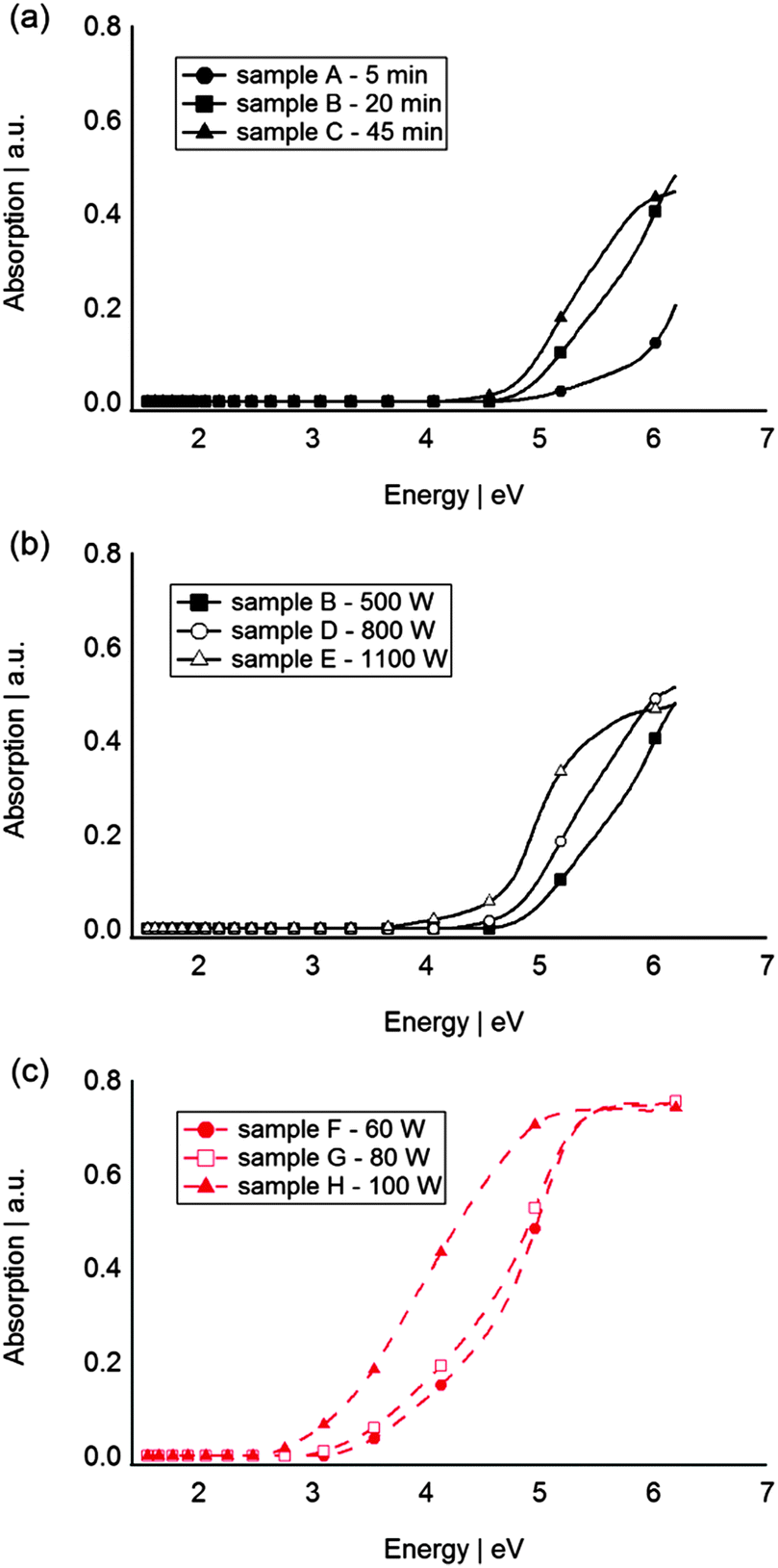 | ||
| Fig. 2 UV-vis absorption spectra of Si QDs synthesised at (a) 500 W for 5, 10 and 20 min, (b) 20 min at 500, 800 and 1100 W, (c) Ge QDs synthesised for 20 min at 60, 80 and 100 W. | ||
From the absorption spectrum, the optical band gap energy (Eg) for the SC QDs can be determined according to the Tauc equation (eqn (1)):48
| αhν = (hν − Eg)n | (1) |
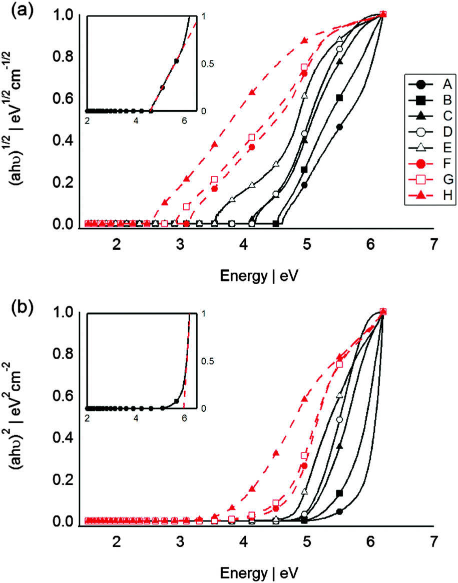 | ||
| Fig. 3 Absorption data for sputtered Si (black line and symbols) and Ge (red dashed lines and symbols) QDs plotted as (a) (ahν)1/2 and (b) (ahν)2, corresponding to an indirect and a direct semiconductors respectively. The inset represents the extrapolation of the curve linear portion (dashed lines) for determination of the band gap. | ||
| Sample | Stoke shifts (eV) | Indirect BG (eV) | Direct BG (eV) | Size based on indirect BG (nm): Si |
|---|---|---|---|---|
| Si: particles size independent of sputtering time | ||||
| A | 0.76 | 4.57 ± 0.03 | 5.96 ± 0.09 | 1.05 ± 0.01 |
| B | 0.70 | 4.51 ± 0.05 | 5.65 ± 0.01 | 1.06 ± 0.01 |
| C | 0.63 | 4.44 ± 0.08 | 5.16 ± 0.05 | 1.08 ± 0.01 |
| Si: QDs size increases with power | ||||
| B | 0.70 | 4.51 ± 0.05 | 5.65 ± 0.01 | 1.06 ± 0.01 |
| D | 0.60 | 4.41 ± 0.03 | 5.10 ± 0.04 | 1.09 ± 0.01 |
| E | 0.45 | 4.26 ± 0.06 | 4.72 ± 0.03 | 1.13 ± 0.01 |
| 3.36 ± 0.04 | 1.44 ± 0.02 | |||
| Ge: BG energy decreases with power | ||||
| F | n/a | 3.04 ± 0.05 | 4.70 ± 0.06 | n/a |
| G | n/a | 2.87 ± 0.06 | 4.61 ± 0.03 | n/a |
| H | n/a | 2.52 ± 0.08 | 3.95 ± 0.05 | n/a |
The sputtering conditions (power applied to the target, time, Ar pressure, etc.) are important factors which can have a great influence on the size of QDs. In our system the influence of the sputtering power and time on the optical properties of QDs were investigated with respect to Si. As Fig. 2a and Table 2 show sputtering for longer time increases the concentration of Si QDs in the PFPE and does not significantly change the size of the particles. Similar behaviour was observed for sputtering metal nanoparticles into ionic liquids. Torimoto et al.,39 Suzuki et al.,50 Hatakeyama et al.51 and Wender et al.46 reported that increasing the sputtering time only yielded an increase of the metal particle concentration without changing the physical size of the particles. However, increasing the power, which is related to the energy and the number of atoms ejected from the target per second, from 500 W to 1100 W is more pronounced in regards to formation of larger particles (similar observations for Ge QDs). The discharge voltage was observed to increase from 448 V to 550 V. Wender et al. also suggested that increasing the discharge voltage, resulted in the formation of larger metal particles in castor oil.52,53
Most of the work that has been conducted in the area of SC QDs has focused on H or O passivation of Si QDs with a limited number of papers investigating the UV-light emission from Si QDs. Wilcoxon et al. reported PL emission in the range of 4.13–1.8 eV for sub-Bohr radius Si passivated with H (excited at 4.84 eV).54 The Bohr radius is used as one measure of the QD size below which confinement effects are typically observed (4.9 and 24.3 nm for Si55 and Ge56 respectively). Yang et al. observed PL emission in the UV-blue region (4.00–2.38 eV) when Si clusters in the 2–5 nm size regime were passivated with alkyl chemistry.57 Tilley et al. reported an emission peak at 3.7 eV for 1.8 nm ± 0.2 nm Si QDs when excited at 4.27 eV.58 Shirahata et al. synthesised silicon terminated hydrocarbon chains with 4.13–2.25 eV PL,59 and emission from passivated Si with alkoxy monolayers in the range of 4.13–2.75 eV.60 These studies suggest the potential of Si QDs in UV light source applications, up to approximately 4.1 eV.
In our system, the Si QDs are covered with F atoms. However, because the F atoms are already bound to the polyether structure, it is assumed that no direct bonding occurs between the Si and F. The high electronegativity of F (3.98) coupled with the small covalent atom radius (0.64 Å, second smallest atom after H) is hypothesised to be the reason why the Si QDs are still observed to behave as if they were directly passivated. F atoms not only can affect the electron cloud of the other atoms it covalently bonds to, but also influences other bonds within its vicinity. This phenomena is referred to the “environmental effect” of an atom on the next nearest neighbours (in this case Si).61 These properties of F is the reason for HF etching resulting in H-terminated Si surfaces rather than F-termination, despite the bond energy of Si–F being nearly twice that of Si–H.62 The prior literature reported band gaps of F passivated Si QDs which are lower than our optically measured band gaps. For instance, Yong et al.31 observed that when F atoms were present on the surface of Si QDs (<2 nm), the band gap energy decreases from the values observed for H passivation. Theoretically calculated band gaps of F passivated Si QDs by Zhou et al. indicates that the electronegativity of F causes an unequal shift of both HOMO and LOMO leading to a decrease in the band gap (again compared to H).63 In all mentioned cases Si QDs were directly passivated by F, however in our system because of the F being bound within the PFPE molecule, the Si QDs are merely in close proximity for F atoms to influence the electronic structure of Si without any direct bonding. It should be noted that PFPE contains O and C atoms and due to the “environmental effect”, the influence of O and C on optical properties of Si QDs cannot be ruled out. Contamination of the surface by O is ruled out, as our synthesis route was conducted in a pure Ar environment, and PFPE has very low solubility for O.64 In addition no H was present during our synthesis process. We hypothesise that in such a confined system, the energies of electrons and holes in the HOMO and LUMO leads to the formation of sub-band energies which provide a possible reason for such an increase in the band gap of the Si QDs. In our system the band gap energies increase with lower sputter power; both these suggest a decreasing in size of Si QDs, and hence consistent with the quantum confinement effect. Commensurate with this is the increasing band gap for Ge QDs, with values determined to be >2.5 eV. This is higher than those previously reported.65
To test the hypothesis of Si and F interaction in the absence of direct bonding, attempts were made to change the surface chemistry of the Si QDs by introducing low partial pressures of O2 gas into the sputtering chamber during deposition. Fig. 4a reports the change of the QD band gap when O2 was added to the system. Two band gaps can be estimated from the sample which was synthesised in Ar and O2. The higher band gap (4.48 eV) is in good agreement with that determined from the previously sputtered QDs at 500 W for 20 min. This is due to the large portion of Si QDs that are completely covered by F atoms (Fig. 4c). The smaller band gap (ca. 3.37 eV) is hypothesised to be for partially O passivated Si QDs (Fig. 4d). Note that isomer α-Si31 was presented in Fig. 4 purely for illustration purposes only, and does not imply any particular crystallinity for the QDs. Likewise, Ge QDs sputtered at 80 W in presence of a mixture of Ar and O2 exhibit two different band gaps (Fig. 4b). Both band gaps, estimated at 3.50 and 4.13 eV, are higher than that of the F-passivated Ge QDs (2.89 eV), and could be indicative of two different partially O passivated Ge QDs. This simple experiment shows that slight changes in surface chemistry of the SC QDs leads to a change of optical properties and confirms the important role of the host matrix in the final properties of the resultant SC QDs. Moreover, the resultant changes in band gap upon matrix passivation are not unique and most likely material dependent as the band gaps of the O passivated Si QDs and O passivated Ge QDs, respectively decreased and increased compared to that of their corresponding F passivated values.
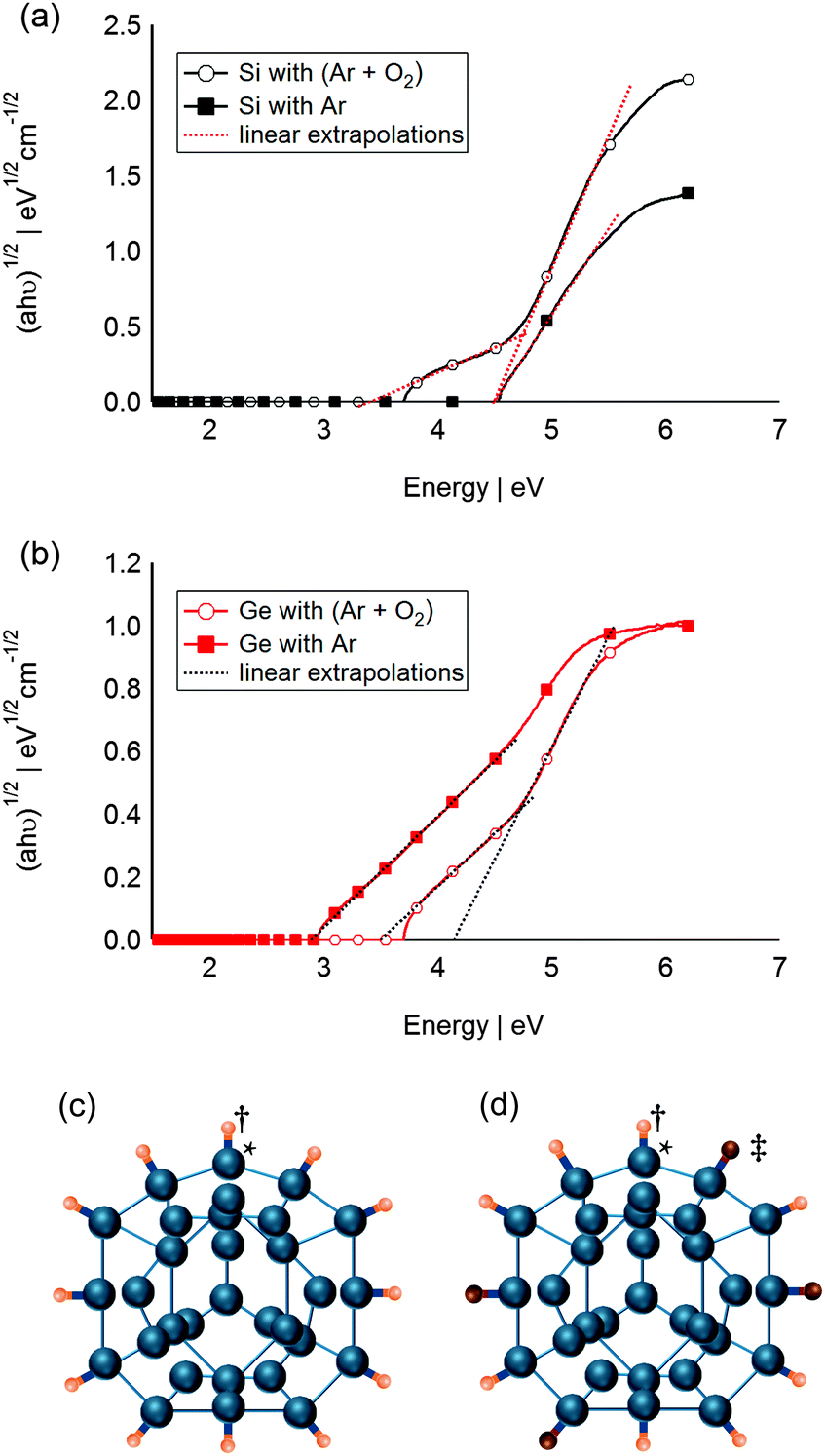 | ||
| Fig. 4 Absorption data for sputtered (a) Si QDs and (b) Ge QDs in Ar environment and Ar and O2 environment plotted as (ahν)1/2, corresponding to an indirect semiconductor. (c) Schematic of F passivated Si QDs, (d) schematic of partially O passivated Si QDs: †, ‡, * represent F atoms, O atoms and Si atoms respectively. Schematic of Si QDs (Si31 α) adapted from ref. 66 purely for illustration purposes. | ||
The PL spectra of all sputtered Si QDs were obtained when excited at 4.95 eV at room temperature. Fig. 5 shows PL peaks centred at 3.81 eV for all of the samples. A long wavelength tail is present in all samples to varying degrees and is hypothesised to arise from different surface chemistries of the QDs. In this case the surface of a sub-population of Si QDs are not perfectly covered by F atoms and partial coverage by C and O atoms of PFPE lead to near UV/blue emission peaks. The PL wavelengths in the UV region is not widely reported for Si, with Shirahata et al. recently commenting that UV emission requires oxide free Si QDs and accurate control of size (<2.5 nm).60 Their observation and the UV emission of the sputtered Si QDs presented here confirm that the Si QDs are required to be not only oxide-free but also smaller than 2.5 nm, in agreement with our size predictions. The PL spectra of sputtered Si QDs shows that increasing sputtering power does not have any influence on the peak light emission. As the size of Si QDs increases in sample E, the PL energy remained constant, suggesting that the effect of surface chemistry prevails over that of quantum confinement in this size regime.
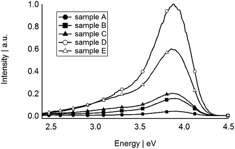 | ||
| Fig. 5 PL spectra of sputtered Si QDs in the PFPE. | ||
Comparing the absorption and emission energies of sputtered Si QDs one can observe that the PL redshifted relative to the absorption. This shift which is also called the Stokes shift defines as (eqn (2)):67
| EStokes = Eabsorption − Eemission | (2) |
There are various reasons for the Stokes shift such as different spatial envelope function symmetry between electron and hole and non-resonant absorption due to presence of large size variation in the sample.68 However, discussion regarding the plausible mechanism for the Stokes shift is outside the scope of this paper.
The calculated Stokes shifts for all samples shows the same behaviour as band gaps. As the size of the cluster increases in sample E, the Stokes shift decreases, similar to the observations of von Behren et al.69 Surface state or self-trapped excitons70 are two possible reasons for increasing Stokes shift with decreasing the size. However the previously reported Stokes shifts show that surface passivation is an important factor in determination of Stokes shifts.67 Sputtered Si QDs shows a Stokes shift up to 0.8 eV which is similar to the calculated Stokes shifts of H passivated Si cluster/QDs by Puzder et al.67 Our hypothesis is that the indirect passivation of Si QDs surface with F atoms is responsible for such a behaviour of Si QDs. Therefore, if quantum confinement was the only reason for the PL by increasing the size of the Si QDs, the PL energy should increase, exactly as predicted by quantum confinement. The constant energies of PL for all of the sputtered samples even with larger size (sample E), can be considered as the effect of surface chemistry. So in this case we believe that surface chemistry is powerful enough to counter the quantum confinement effect.
Conclusions
In conclusion, we have presented the synthesis of SC QDs using DC magnetron sputtering into negligible vapour pressure, transparent PFPE oil. This combination allows for independent control of the QD size (sputtering conditions) and surface passivation (liquid chemistry and partial pressure gases in the sputter chamber). As a result very high band gaps for Si QDs are realised when the size approaches 1 nm and passivated with F. Ge QDs have shown higher band gaps when O passivated. In the case of Si QDs, the PL has been observed in the UV region, without doping or direct passivation of the QD surface. The ability to simply synthesise pristine SC QDs and tune their optical properties through surface chemistry and/or confinement effects opens opportunities for their use in a range of high energy (optical or thermal) applications.Acknowledgements
This original research was proudly supported by the Commonwealth of Australia, through the Automotive Australia 2020 Cooperative Research Centre (AA2020CRC). This research was partly supported under Australian Research Council's Linkage Infrastructure, Equipment and Facilities funding scheme (project LE140100033).References
- M. Hybertsen, in Porous Silicon Science and Technology, ed. J.-C. Vial and J. Derrien, Springer, Berlin, 1995, vol. 5, pp. 67–90 Search PubMed.
- A. M. Fox, Optical properties of solids, Oxford University Press, USA, 2001 Search PubMed.
- E. F. Schubert and J. K. Kim, Science, 2005, 308, 1274–1278 CrossRef CAS PubMed.
- K. Kim, J. Li, S. Jin, J. Lin and H. Jiang, Appl. Phys. Lett., 2003, 83, 566–568 CrossRef CAS.
- T. Nishida, H. Saito and N. Kobayashi, Appl. Phys. Lett., 2001, 79, 711–712 CrossRef CAS.
- M. Kneissl, in III-Nitride Ultraviolet Emitters: Technology and Applications, ed. M. Kneissl and J. Rass, Springer, New York, 2015, pp. 3–4 Search PubMed.
- L. Canham, Appl. Phys. Lett., 1990, 57, 1046–1048 CrossRef CAS.
- N. Koshida and H. Koyama, Jpn. J. Appl. Phys., 1991, 30, L1221 CrossRef CAS.
- D. J. Lockwood and A. G. Wang, Solid State Commun., 1995, 94, 905–909 CrossRef CAS.
- A. Cullis, L. Canham and P. Calcott, J. Appl. Phys., 1997, 82, 909–965 CrossRef CAS.
- K. Sattler, in Handbook of Thin Films Materials, Nanomaterials and Magnetic Thin Films, ed. H. S. Nalwa, Academic Press, 2002, vol. 2, pp. 61–97 Search PubMed.
- C. Delerue, G. Allan and M. Lannoo, Phys. Rev. B: Condens. Matter Mater. Phys., 1993, 48, 11024 CrossRef CAS.
- J. Wang, H.-B. Jiang, W.-C. Wang, J.-B. Zheng, F.-L. Zhang, P.-H. Hao, X.-Y. Hou and X. Wang, Phys. Rev. Lett., 1992, 69, 3252 CrossRef CAS PubMed.
- P. Trwoga, A. Kenyon and C. Pitt, J. Appl. Phys., 1998, 83, 3789–3794 CrossRef CAS.
- D. Lockwood, A. Wang and B. Bryskiewicz, Solid State Commun., 1994, 89, 587–589 CrossRef CAS.
- A. Puzder, A. Williamson, J. C. Grossman and G. Galli, Phys. Rev. Lett., 2002, 88, 097401 CrossRef PubMed.
- M. Wolkin, J. Jorne, P. Fauchet, G. Allan and C. Delerue, Phys. Rev. Lett., 1999, 82, 197 CrossRef CAS.
- M. Tischler, R. Collins, J. Stathis and J. Tsang, Appl. Phys. Lett., 1992, 60, 639–641 CrossRef CAS.
- L. Chiu, A. Seraphin and K. Kolenbrander, J. Electron. Mater., 1994, 23, 347–354 CrossRef CAS.
- B. Marsen, M. Lonfat, P. Scheier and K. Sattler, Phys. Rev. B: Condens. Matter Mater. Phys., 2000, 62, 6892 CrossRef CAS.
- V. Ranjan, M. Kapoor and V. A. Singh, J. Phys.: Condens. Matter, 2002, 14, 6647 CrossRef CAS.
- W. Little, A. Karatutlu, D. Bolmatov, K. Trachenko, A. Sapelkin, G. Cibin, R. Taylor, F. Mosselmans, A. Dent and G. Mountjoy, Sci. Rep., 2014, 4, 7372 CrossRef CAS PubMed.
- Y. Ma, X. Chen, X. Pi and D. Yang, J. Phys. Chem. C, 2011, 115, 12822–12825 CAS.
- D. König, J. Rudd, M. A. Green and G. Conibeer, Phys. Rev. B: Condens. Matter Mater. Phys., 2008, 78, 035339 CrossRef.
- C. Tsai, K. H. Li, J. Sarathy, S. Shih, J. Campbell, B. Hance and J. White, Appl. Phys. Lett., 1991, 59, 2814–2816 CrossRef CAS.
- I. Vasiliev, J. R. Chelikowsky and R. M. Martin, Phys. Rev. B: Condens. Matter Mater. Phys., 2002, 65, 121302 CrossRef.
- Z. Zhou, L. Brus and R. Friesner, Nano Lett., 2003, 3, 163–167 CrossRef CAS.
- X. Wang, J. Zhang, L. Ding, B. Cheng, W. Ge, J. Yu and Q. Wang, Phys. Rev. B: Condens. Matter Mater. Phys., 2005, 72, 195313 CrossRef.
- T. Torchynska, J. Non-Cryst. Solids, 2006, 352, 2484–2487 CrossRef CAS.
- A. Zimina, S. Eisebitt, W. Eberhardt, J. Heitmann and M. Zacharias, Appl. Phys. Lett., 2006, 88, 163103 CrossRef.
- Y. Ma, X. Pi and D. Yang, J. Phys. Chem. C, 2012, 116, 5401–5406 CAS.
- O. Wolf, M. Dasog, Z. Yang, I. Balberg, J. Veinot and O. Millo, Nano Lett., 2013, 13, 2516–2521 CrossRef CAS PubMed.
- J. G. Veinot, Chem. Commun., 2006, 4160–4168 RSC.
- G. Qin, G. Ran, K. Sun and H. Xu, J. Nanosci. Nanotechnol., 2010, 10, 1584–1595 CrossRef CAS PubMed.
- K. Dohnalová, T. Gregorkiewicz and K. Kůsová, J. Phys.: Condens. Matter, 2014, 26, 173201 CrossRef PubMed.
- S. Askari, V. Svrcek, P. Maguire and D. Mariotti, Adv. Mater., 2015, 27, 8011–8016 CrossRef CAS PubMed.
- A. Sadegh, M.-M. Manuel, V. Tamilselvan, M. Paul, S. Vladmir and M. Davide, J. Phys. D: Appl. Phys., 2015, 48, 314002 CrossRef.
- L. Valeri, J. Phys. D: Appl. Phys., 2011, 44, 174013 CrossRef.
- T. Torimoto, K.-i. Okazaki, T. Kiyama, K. Hirahara, N. Tanaka and S. Kuwabata, Appl. Phys. Lett., 2006, 89, 243117 CrossRef.
- D. König, K. Richter, A. Siegel, A. V. Mudring and A. Ludwig, Adv. Funct. Mater., 2014, 24, 2049–2056 CrossRef.
- K.-I. Okazaki, T. Kiyama, K. Hirahara, N. Tanaka, S. Kuwabata and T. Torimoto, Chem. Commun., 2008, 691–693 RSC.
- Y. Hatakeyama, K. Onishi and K. Nishikawa, RSC Adv., 2011, 1, 1815–1821 RSC.
- T. Tsuda, T. Kurihara, Y. Hoshino, T. Kiyama, K.-i. Okazaki, T. Torimoto and S. Kuwabata, Electrochemistry, 2009, 77, 693–695 CrossRef CAS.
- H. Yoshida, K. Kawamoto, H. Kubo, T. Tsuda, A. Fujii, S. Kuwabata and M. Ozaki, Adv. Mater., 2010, 22, 622–626 CrossRef CAS PubMed.
- H. Najafov, B. Lee, Q. Zhou, L. Feldman and V. Podzorov, Nat. Mater., 2010, 9, 938–943 CrossRef CAS PubMed.
- H. Wender, L. F. de Oliveira, P. Migowski, A. F. Feil, E. Lissner, M. H. Prechtl, S. R. Teixeira and J. Dupont, J. Phys. Chem. C, 2010, 114, 11764–11768 CAS.
- J. Humlicek and E. Kasper, The Institute of Electrical Engineers, INSPEC, London, UK, 1995, p. 121 Search PubMed.
- J. Tauc and A. Menth, J. Non-Cryst. Solids, 1972, 8, 569–585 CrossRef.
- C. Meier, A. Gondorf, S. Lüttjohann, A. Lorke and H. Wiggers, J. Appl. Phys., 2007, 101, 103112 CrossRef.
- T. Suzuki, K.-I. Okazaki, T. Kiyama, S. Kuwabata and T. Torimoto, Electrochemistry, 2009, 77, 636–638 CrossRef CAS.
- Y. Hatakeyama, S. Takahashi and K. Nishikawa, J. Phys. Chem. C, 2010, 114, 11098–11102 CAS.
- H. Wender, R. V. Gonalves, A. F. Feil, P. Migowski, F. S. Poletto, A. R. Pohlmann, J. Dupont and S. R. Teixeira, J. Phys. Chem. C, 2011, 115, 16362–16367 CAS.
- H. Wender, L. F. de Oliveira, A. F. Feil, E. Lissner, P. Migowski, M. R. Meneghetti, S. R. Teixeira and J. Dupont, Chem. Commun., 2010, 46, 7019–7021 RSC.
- J. Wilcoxon, G. Samara and P. Provencio, Phys. Rev. B: Condens. Matter Mater. Phys., 1999, 60, 2704 CrossRef CAS.
- A. A. Ischenko, G. V. Fetisov and L. A. Aslalnov, Nanosilicon: properties, synthesis, applications, methods of analysis and control, CRC Press, New York, 2014 Search PubMed.
- Y. Maeda, N. Tsukamoto, Y. Yazawa, Y. Kanemitsu and Y. Masumoto, Appl. Phys. Lett., 1991, 59, 3168–3170 CrossRef CAS.
- C.-S. Yang, R. A. Bley, S. M. Kauzlarich, H. W. Lee and G. R. Delgado, J. Am. Chem. Soc., 1999, 121, 5191–5195 CrossRef CAS.
- R. D. Tilley, J. H. Warner, K. Yamamoto, I. Matsui and H. Fujimori, Chem. Commun., 2005, 1833–1835 RSC.
- N. Shirahata, M. R. Linford, S. Furumi, L. Pei, Y. Sakka, R. J. Gates and M. C. Asplund, Chem. Commun., 2009, 4684–4686 RSC.
- N. Shirahata, T. Hasegawa, Y. Sakka and T. Tsuruoka, Small, 2010, 6, 915–921 CrossRef CAS PubMed.
- R. Zhang, Y. Zhao and B. K. Teo, Phys. Rev. B: Condens. Matter Mater. Phys., 2004, 69, 125319 CrossRef.
- G. Trucks, K. Raghavachari, G. Higashi and Y. Chabal, Phys. Rev. Lett., 1990, 65, 504 CrossRef CAS PubMed.
- Z. Zhou, R. A. Friesner and L. Brus, J. Am. Chem. Soc., 2003, 125, 15599–15607 CrossRef CAS PubMed.
- U. Wallfahrer, in Synthetics, mineral oils, and bio-based lubricants: chemistry and technology, ed. L. R. Rudnick, CRC press, New York, 2013, vol. 5, p. 192 Search PubMed.
- D. A. Ruddy, J. C. Johnson, E. R. Smith and N. R. Neale, ACS Nano, 2010, 4, 7459–7466 CrossRef CAS PubMed.
- L.-Z. Zhao, W.-C. Lu, W. Qin, C. Wang and K. Ho, J. Phys. Chem. A, 2008, 112, 5815–5823 CrossRef CAS PubMed.
- A. Puzder, A. J. Williamson, J. C. Grossman and G. Galli, J. Am. Chem. Soc., 2003, 125, 2786–2791 CrossRef CAS PubMed.
- D. O. Demchenko and L.-W. Wang, Phys. Rev. B: Condens. Matter Mater. Phys., 2006, 73, 155326 CrossRef.
- J. Von Behren, T. Van Buuren, M. Zacharias, E. Chimowitz and P. Fauchet, Solid State Commun., 1998, 105, 317–322 CrossRef CAS.
- G. Allan, C. Delerue and M. Lannoo, Phys. Rev. Lett., 1996, 76, 2961 CrossRef CAS PubMed.
| This journal is © the Owner Societies 2016 |