
 Open Access Article
 This Open Access Article is licensed under a
 Creative Commons Attribution 3.0 Unported Licence
Fluorescence enhancement in visible light: dielectric or noble metal?†
S.
Sun
 ,
L.
Wu
,
P.
Bai
* and
C. E.
Png
,
L.
Wu
,
P.
Bai
* and
C. E.
Png
Electronics and Photonics Department, Institute of High Performance Computing, Agency for Science, Technology and Research, 138632, Singapore. E-mail: baiping@ihpc.a-star.edu.sg
First published on 24th June 2016
Abstract
A high permittivity dielectric gives the impression of outperforming plasmonic noble metal in visible light fluorescence enhancement primarily because of its small loss. Nonetheless, the performances of these two platforms in various situations remain obscure due to the different optical confinement mechanisms as well as the complexity in the fluorescence enhancement process. This study presents a comprehensive comparison between these two platforms based on nanoparticles (NPs) to evaluate their capability and applicability in fluorescence enhancement by taking into account the fluorescence excitation rate, the quantum yield, the fluorophore wavelengths and Stokes shifts as well as the far field intensity. In a low permittivity sensing medium (e.g. air), the dielectric NP can achieve comparable or higher fluorescence enhancement than the metal NP due to its decent NP-enhanced excitation rate and larger quantum yield. In a relatively high permittivity sensing medium (e.g. water), however, there is a significant decrement of the excitation rate of the dielectric NP as the permittivity contrast decreases, leading to a smaller fluorescence enhancement compared to the metallic counterpart. Combining the fluorescence enhancement and the far field intensity studies, we further conclude that for both dielectric and plasmonic NPs, the optimal situation occurs when the fluorescence excitation wavelength, the fluorescence emission wavelength and the electric-dipole-mode of the dielectric NP (or the plasmonic resonance of the metal NP) are the same and all fall in the low conductivity region of the NP material. We also find that the electric-dipole-mode of the dielectric NP performs better than the magnetic-dipole-mode for fluorescence enhancement applications because only the electric-dipole-mode can be strongly excited by the routinely used fluorescent dyes and quantum dots, which behave as electric dipoles by nature.
Introduction
Fluorescence is one of the most widespread optical techniques for the detection of molecular analytes in chemistry, biology, materials science and medicine over several decades.1,2 In routinely used fluorescence assays, fluorophores such as organic dyes or quantum dots commonly serve as labels for the target analytes attached with molecular recognition elements.3 However, the optical signal from a single fluorophore is generally weak hence limits the sensitivity.4 This problem becomes critical in those applications that directly rely on efficient detection of emission from a single fluorophore, such as DNA sequencing,5,6 molecular and cell biology,7 early diagnosis,8 drug screening,9 and safety assessment in food and environmental industry,10 among others. Driven by the increasing demand in these emerging fields, technologies in amplifying the fluorescence signal attract great attention worldwide and are consistently pursued to improve the sensitivity.Noble metals such as Au and Ag have been proven to be a versatile platform in fluorescence enhancement. Owing to the collective electron oscillation at the metallic surface, the so-called surface plasmon resonance (SPR), metal nanostructures can effectively confine the optical energy into the sub-wavelength region.11,12 Such confinement creates a strong near field enhancement in the vicinity of the nanostructure, which provides the foundation for enhancing the fluorescence excitation rate.13–15 Moreover, introducing the metallic nanostructure tailors the surrounding environment of the fluorophore, enabling the manipulation of directivity of the fluorescence emission.16–18 To date, a routine procedure has been developed to coat the plasmonic nanostructures with multiple ligands to dramatically increase the uptake and retention of fluorescence emitters.19 The fluorescence intensity can be significantly enhanced,20–24 while highly directional emission17,18,25–28 has also been achieved. Despite all the successful stories, plasmonic platforms suffer large parasitic losses inherent to the intrinsic high conductivities of the metallic materials, which compromise the quantum yields of fluorescence emitters particularly when the fluorophores are close to the metallic surface (also known as quenching).14,29–34 Consequently, the reduction in the quantum yield counteracts the plasmonic-enhanced fluorescence excitation rate, and the maximum fluorescence enhancement can only be achieved at a moderate distance (∼10 nm) away from the metal surface.29,30,35–38
To avoid the limitation of high loss in metals, high permittivity dielectrics (e.g. Si,39–46 GaAs,47 and GaP,48 among others49,50) have been recently proposed as an alternative platform to enhance the fluorescence. The high permittivity contrast between the dielectric and the surrounding medium grants the capability of optical confinement.42,44 Such confinement, although different from that of plasmonic metal in terms of the physical mechanism, also leads to enhancement in the near field and consequently the fluorescence excitation rate.44,49 Moreover, the loss-less nature of dielectric materials naturally results in larger quantum yields than plasmonic metals.42,44,50 In addition, dielectric nanostructures can also modify the fluorescence directivity similar to the plasmonic nanostructures.39,40,43,47 The dielectric nanostructures are able to excite both the electric-dipole-mode (ED) and magnetic-dipole-mode (MD) whereby the metallic counterparts only excite the electrical-natured SPR.40–44 Other features such as low thermal conversion46,48 and compatibility with CMOS technology contribute additional merits in terms of cost, stability and reliability.
Nevertheless, previous studies focus on analyzing the fundamental modes41,45,47 of the dielectric nanostructure and how these modes are coupled with the fluorescence emitters.39,40,42,44 A comprehensive investigation on the fluorescence enhancement combining the excitation rate and quantum yield, which has been well revealed for the plasmonic nanostructures,29,30,36,37 is still missing for the dielectric nanostructure. As a result, up to now, there is no general conclusion about which platform has better performance in fluorescence enhancement. In fact in the visible light spectrum, the loss-less natures of dielectrics do not always hold true particularly at short wavelengths. How will the presence of loss affect the applicability of dielectrics in visible light fluorescence enhancement (popular in bio-sensing, where it can be easily detected with a CCD camera)? More critically, the mechanisms of optical confinement between dielectric44 and plasmonic11 NPs are entirely different. How will the different mechanisms affect their relative performances in different sensing mediums (e.g. air or water)? To address these questions, a comparison of fluorescence enhancement in various situations between dielectrics and plasmonic metal must be conducted.
For the fluorescence enhancement, two primary parameters are essential: the fluorescence excitation rate and the quantum yield.29,37 First, the fluorescence excitation rate directly relates to the near field enhancement which reaches maximum at the resonance wavelength of the nanostructure. Therefore, an appropriate comparison in fluorescence enhancement should be conducted when the resonance wavelengths of both the dielectric and plasmonic nanostructures are aligned with the excitation wavelength of the fluorophore. Second, the quantum yield describes the probability of a fluorescence photon that can emit to the far field, which highly relies on the materials as well as the distance between the fluorophore and the nanostructure. Their respective optimized distances where the maximum fluorescence enhancements arise thus need to be identified for the dielectric and plasmonic nanostructure. Besides, the fluorescence Stokes shift (the separation between the fluorescence excitation wavelength and emission wavelength) can also affect the fluorescence enhancement, which should be taken into account. Lastly, at the maximum fluorescence enhancement where the fluorescence excitation rate and quantum yield have already been well balanced, the far field intensity should be monitored as it can be measurable.
In this contribution, we present a comprehensive evaluation on the capability and applicability of dielectrics and plasmonic metal nanoparticles (NPs) in fluorescence enhancement in the visible light regime, because the NPs are the most fundamental nanostructures with well-defined resonance modes that allow us to clearly assess the physical insight. To this end, we first investigate the dielectric/plasmonic NP-enhanced fluorescence in air medium. The respective fluorescence enhancements produced by the plasmonic NPs as well as both the ED and MD of the dielectric NPs are compared. The same procedure is employed to study the fluorescence enhancement in water medium, whereby the effects of different physical mechanisms in the optical confinements between the dielectric and plasmonic NPs are revealed. In the comparison, the fluorescence wavelengths and Stokes shifts are also discussed. Moreover, the far field intensity is investigated at the maximum fluorescence enhancement to provide additional insight into the relative performances of the dielectric ED, dielectric MD, and plasmonic resonance mode. In the end, we briefly assess the applicability of some commonly used dielectrics in air and water media. Our calculations are based on a rigorous analytical solution,37,42,51,52 and verified with finite element simulation.
Results
Fig. 1 schematically illustrates the model to calculate the fluorescence enhancement, including the fluorescence excitation process and the fluorescence emission process.37 During the fluorescence excitation process (Fig. 1a), a plane wave at the fluorescence excitation wavelength λext is illuminated to the NP to create a near field enhancement at the location of the fluorophore (a distance x away from the NP surface). Such a strong near field enhancement in turn boosts electrons from the ground state to the higher energy state in a fluorescence emitter, resulting in a NP-enhanced fluorescence excitation rate γext/γ0ext. On the other hand, during the fluorescence emission process (Fig. 1b), the fluorophore itself (e.g. dyes and quantum dots) is treated as an electric dipole source at the emission wavelength λem. Photons emitted from the dipole source can either decay radiatively to the far field or non-radiatively to the loss. The quantum yield q/q0 accounts for the competition between the radiative decay rate Γr/Γ0 and the non-radiative decay rate Γnr/Γ0, which represents the probability of a fluorescence photon that can emit to the far field. The fluorescence enhancement ηem/η0em can be subsequently obtained as the product of γext/γ0ext and q/q0 (refer to the Methods section for calculation details).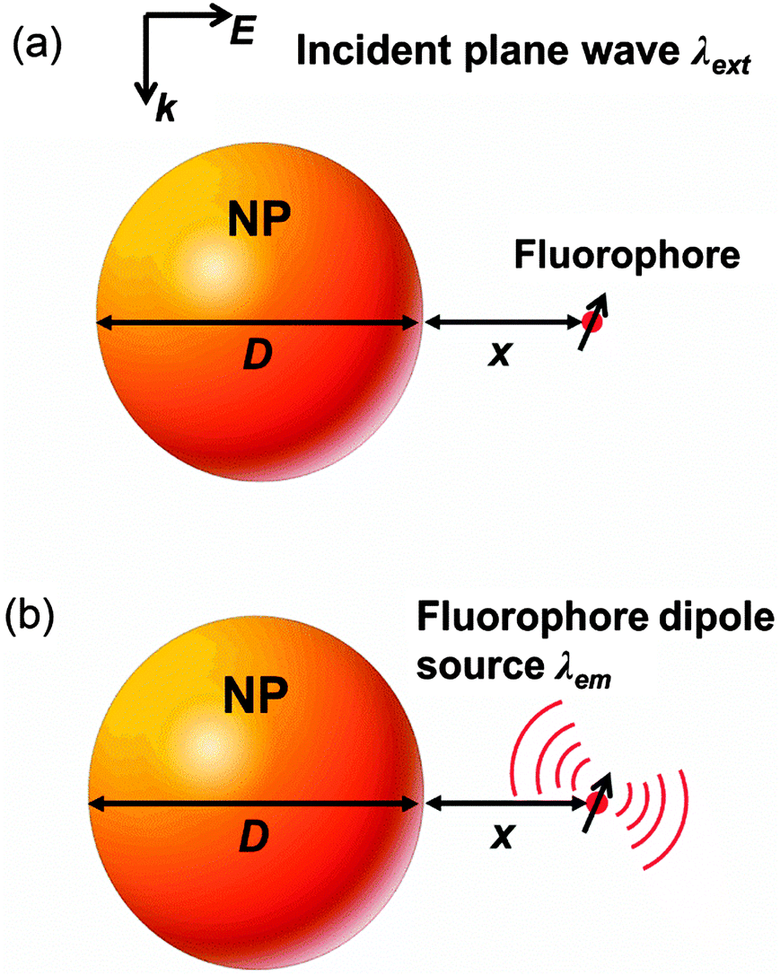 | ||
| Fig. 1 (a) Schematic of the NP-enhanced excitation rate by an incident plane wave at the fluorescence excitation wavelength λext. (b) Schematic of the interaction between the NP and fluorescence emission, whereby the fluorophore is modelled as a dipole source at the emission wavelength λem. | ||
Herein, we use either Ag or Au for the plasmonic metal depending on the fluorophore wavelength (e.g. the plasmonic resonance of the Ag NP is typically around 400–500 nm in air, whereas that of the Au NP is generally larger than 500 nm), and Si to represent the dielectric material due its relatively high permittivity (14–30 in the visible light region). Other commonly used dielectrics are addressed in the Discussion section. The material properties are taken from experimental measurements.53 Two common sensing media are focused on here: (1) air medium with a lower permittivity = 1, which mimics the situation that the solvent is dried out after the fluorophore is bonded to the NP; and (2) water medium with a higher permittivity = 1.77, which mimics the situation that the fluorophore is contained in a solvent.
Fluorescence enhancement in the air medium
To start, we use a fluorophore with a short excitation wavelength λext = 445 nm for illustration, which coincides with the plasmonic resonance (SPR) of a 130 nm in diameter Ag NP, the electric-dipole-mode (ED) of a 125 nm Si NP, or the magnetic-dipole-mode (MD) of a 90 nm Si NP in the air medium as shown in Fig. 2a. The details of the mode compositions of the NPs are presented in Fig. S1 in the ESI.† The enhanced fluorescence excitation rate γext/γ0ext with respect to the location of the fluorophore is depicted in Fig. 2b. Clearly, the excitation rates decreases as x increases because of the evanescent nature of the near field in the vicinity of the NP regardless of whether it is plasmonic or dielectric. The excitation rate produced by the Ag NP is stronger than those produced by the Si ED and MD, which is consistent with the reports in the literature.44,48 Nevertheless, owing to the high permittivity contrast to the air medium, both the ED and MD of the Si NP can still provide decent excitation rates.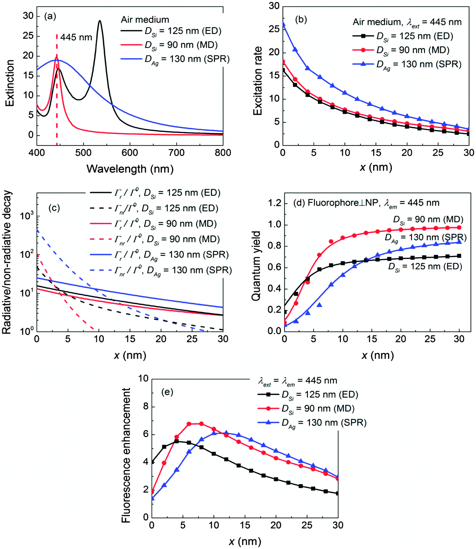 | ||
| Fig. 2 Fluorescence enhancement at a short wavelength (445 nm) in the air medium. (a) The extinction spectrum of the NPs. The electric-dipole-mode (ED) of 125 nm Si, the magnetic-dipole-mode (MD) of 90 nm Si, and the plasmonic resonance (SPR) of 130 nm Ag are all located at λext = 445 nm. (b) The NP-enhanced fluorescence excitation rate γext/γ0ext with respect to the location of the fluorophore. The Ag NP produces a relatively stronger γext/γ0ext than that of the Si NP. Both the ED and MD of the Si NP can provide decent excitation rates due to the high permittivity contrast. (c) The radiative/non-radiative decay rates and (d) the quantum yield q/q0 for the fluorophore oriented perpendicular (⊥) to the NP. q/q0 of the Si NP (both ED and MD) are higher than that of the Ag NP, particularly at x < 14 nm. The relative magnitudes of decay rates show that Ag SPR > Si ED > Si MD because a perpendicular electric dipole can strongly and directly excite the SPR of the Ag NP as well as the ED of the dielectric NP. (e) The fluorescence enhancement ηem/η0em at λext = λem = 445 nm. Due to its moderately high NP-enhanced excitation rate and a larger quantum yield, the Si NP (both ED and MD) can produce a comparable or even higher ηem/η0em as compared to the Ag NP in the air medium. The solid curves are obtained based on the analytical solution, and the symbols are results from finite element simulation using COMSOL Multiphysics. | ||
To obtain the quantum yield, we assume that λem = λext = 445 nm which mimics blue fluorophores with small Stokes shifts (e.g. STOX Blue-DNA, POPO-1-DNA).54 Fluorophores with large Stokes shifts are discussed in the Discussion section. The corresponding radiative decay rates Γr/Γ0 (solid lines) and non-radiative decay rates Γnr/Γ0 (dashed lines) are shown in Fig. 2c for the fluorophore oriented perpendicular (⊥) to the NP. Generally, the relative magnitudes of decay rates (both Γr/Γ0 and Γnr/Γ0) appear to be Ag SPR > Si ED > Si MD because a perpendicular electric dipole can strongly excite the SPR of the Ag NP and the ED of the Si NP.42 More details can be found in Fig. S1 in the ESI.† Moreover, the non-radiative components Γnr/Γ0 are significant not only for the Ag NP, but also for the Si NP especially when the fluorophore is close to the NP (x < 5 nm). This is attributed to the significant increment in the conductivity of Si below 550 nm, leading to a non-negligible loss at λem = 445 nm (Si has a bandgap ∼1.1 eV, hence it is not loss-less at 445 nm). The presence of loss in turn leads to the diminishing feature of the quantum yield q/q0 as x decreases as shown in Fig. 2d. Details of the Si conductivity profile are shown in Fig. S2 in the ESI.† Nevertheless, Γnr/Γ0 of the Si NP is still much weaker as compared to that of the Ag NP, therefore the quantum yields q/q0 of the Si NP (both ED and MD) are still higher than that of the Ag NP in particular for x < 14 nm.
For the fluorophore oriented parallel (‖) to the NP, the respective decay rates (both Γr/Γ0 and Γnr/Γ0) and quantum yield q/q0 of the three NPs are much smaller as compared to those for the fluorophore⊥NP. Especially the radiative decay rates Γr/Γ0 drop approximately one order of magnitude because a parallel electric dipole can only weakly excite the MD of the dielectric NP, but has a negligible effect on the SPR of the Ag NP or the ED of the dielectric NP.42 Details are shown in Fig. S3 in the ESI.† This clearly indicates that the maximum fluorescence enhancement as well as the highest radiative decay rate can only be achieved when the fluorophore aligns perpendicular to the NP. Therefore, we focus on discussing the fluorophore⊥NP hereafter.
The fluorescence enhancement ηem/η0em is shown in Fig. 2e. Clearly in the air medium, even at a relatively high loss wavelength (e.g. λem = λext = 445 nm), the Si NP (both ED and MD) can produce a comparable or even higher ηem/η0em as compared to that of the Ag NP, owing to its moderately high NP-enhanced excitation rate and a larger quantum yield. The optimal distance to achieve the maximum ηem/η0em is shorter for the Si NP (e.g. x = 4 nm for ED, and 6 nm for MD), whereas it must be longer for the Ag NP (x = 12 nm) to avoid quenching.
Recall that the diminishing feature of quantum yield q/q0 in Fig. 2d originates from the relatively high conductivity of Si at 445 nm, which induces a large non-radiative decay rate in particular at a short distance. Based on this principle, selecting the fluorophore emission wavelength at the low conductivity region of Si could further improve the quantum yield and fluorescence enhancement.
This concept is proven at the yellow fluorophore wavelength λext = λem = 550 nm (e.g. Alexa 555, Cy3),54 which corresponds to the ED of 175 nm Si, the MD of 130 nm Si, and the SPR of 160 nm Au as shown in Fig. 3a. The detailed mode composition is shown in Fig. S4 in the ESI.† The NP-enhanced excitation rates γext/γ0ext are illustrated in Fig. 3b. Again, although the Au NP demonstrates the largest γext/γ0ext, the Si ED and MD can still produce decent excitation rates due to the high permittivity contrast to the air medium. At 550 nm, the conductivity of Si drops 82% as compared to that at 445 nm. Therefore, the non-radiative decay rates Γnr/Γ0 (Fig. 3c) of both the Si ED and MD at 550 nm have been significantly suppressed as compared to those at 445 nm. Meanwhile, the radiative decay components Γr/Γ0 of the Si ED and MD are maintained at similar levels to those at 445 nm. As a result, the quantum yields q/q0 of the Si NP are greatly improved in particular for the Si ED, which are much higher than that of the Au NP (Fig. 3d). The fluorescence enhancements in Fig. 3e clearly verify that ηem/η0em can be further improved (e.g. 33% increment for the Si MD and 79.1% increment for the Si ED at 550 nm as compared to those at 445 nm) by selecting the fluorescence emission wavelength at the low conductivity region of Si. The same conclusion also holds at longer wavelengths since the conductivity of Si remains low for a wavelength >550 nm.
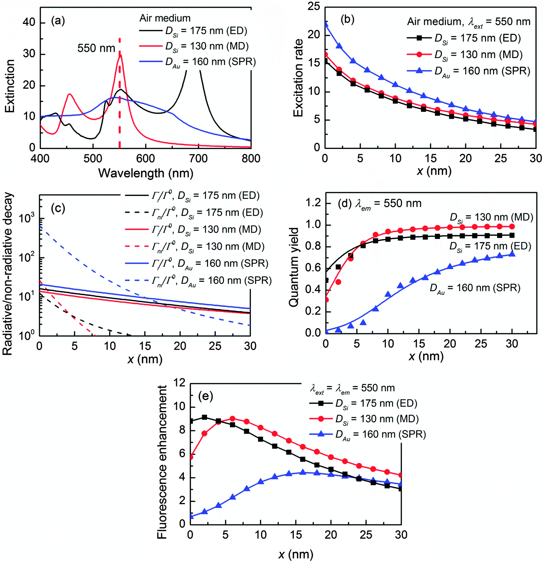 | ||
| Fig. 3 Fluorescence enhancement at a longer wavelength (550 nm) in the air medium. (a) The extinction spectrum of the NP. The electric-dipole-mode (ED) of 175 nm Si, the magnetic-dipole-mode (MD) of 130 nm Si, and the plasmonic resonance (SPR) of 160 nm Au are all located at a fluorescence excitation wavelength λext = 550 nm. (b) The NP-enhanced fluorescence excitation rate γext/γ0ext with respect to the location of the fluorophore. (c) The radiative and non-radiative decay rates and (d) the quantum yield at the fluorescence emission wavelength λem = 550 nm. The non-radiative decay rates Γnr/Γ0 of both the Si ED and MD have been greatly suppressed due to the low conductivity of Si at 550 nm (82% decrement as compared to that at 445 nm). The quantum yields q/q0 of the Si NP are thus improved, especially for the ED. (e) The fluorescence enhancements ηem/η0em can be improved by selecting the fluorescence emission wavelength at the low conductivity region of Si. | ||
The idea to boost the quantum yield by suppressing the non-radiative decay rate can also be adapted to the plasmonic NPs, which perform particularly well for the Au NPs. The conductivity of Au decreases dramatically as the wavelength increases in the visible light region. As a result, the loss of Au NPs can be greatly reduced for a fluorophore emission wavelength λem ≥ 600 nm, and the quantum yield can be significantly enhanced. In fact, experiments also demonstrated that Au is well suited for red fluorophore enhancement such as Cy555 and Alexa 647,20,56,57 which is not only because of the strong SPR-enhanced excitation rate but also due to its relatively low loss at these wavelengths. On the other hand, the conductivity of Ag is approximately constant over the visible light region, thus its quantum yield does not change much at different wavelengths. More details can be found in Fig. S5 in the ESI.†
Fluorescence enhancement in the water medium
As the permittivity of the sensing medium increases, the dielectric NP and plasmonic NP response is different since their physical mechanisms of optical confinements are entirely different. For the dielectric NP whose real part permittivity is positive, its optical confinement is obtained by generating intense displacement current inside the NP which essentially results from the permittivity contrast between the NP material and the surrounding medium.44,58 Increasing the permittivity of the medium naturally leads to a decrement in the permittivity contrast and consequently a weaker optical confinement. On the other hand for the plasmonic NP, its optical confinement is created by collective oscillation of electrons which is represented by a negative real part permittivity.2,12 Increasing the permittivity of the medium in principle would enhance the permittivity contrast and establish a stronger optical confinement.The effect of the sensing medium can be demonstrated for fluorescence emission (λext = λem = 550 nm, where the conductivity of Si is already low and its non-radiative decay rate has been suppressed) in the water medium (permittivity = 1.77), which corresponds to the ED of a 165 nm Si NP, the MD of a 130 nm NP, and the SPR of a 125 nm Ag NP as shown in Fig. 4a. The detailed mode composition is shown in Fig. S6 in the ESI.† The NP-enhanced excitation rates γext/γ0ext are depicted in Fig. 4b. Apparently, γext/γ0ext of the Si NP decreases tremendously (especially for the Si ED) as compared to those in the air medium (Fig. 3b) and becomes much smaller than that of the Ag NP. Besides the excitation rate, the radiative decay rates Γr/Γ0 of the Si NP as shown in Fig. 4c also decrease significantly as compared to those in the air medium (Fig. 3c). In particular, Γr/Γ0 of the Si ED drops 53.3%, while that of the Si MD drops 17%. This is because the Si ED is more sensitive to the change of the sensing medium than the Si MD is, and the Si ED will completely disappear in the extinction spectrum at an even higher medium permittivity = 2.25 (oil).58 More details can be found in Fig. S7 in the ESI.† Nevertheless, the quantum yield q/q0 of the Si NP remains higher than that of the Ag NP as shown in Fig. 4d due to the low conductivity of Si at 550 nm. However this time, the high quantum yield is not enough to compensate the decrement in the excitation rate for the Si NP. As a result, the fluorescence enhancements ηem/η0em of the Si NP are weaker than that of the Ag NP, which is shown in Fig. 4e. Another example is presented at a red fluorophore λext = λem = 650 nm in Fig. S8 in the ESI,† whereby the Au NP possess a higher fluorescence enhancement than those of the Si NP. The same conclusion can also be extended to other wavelengths.
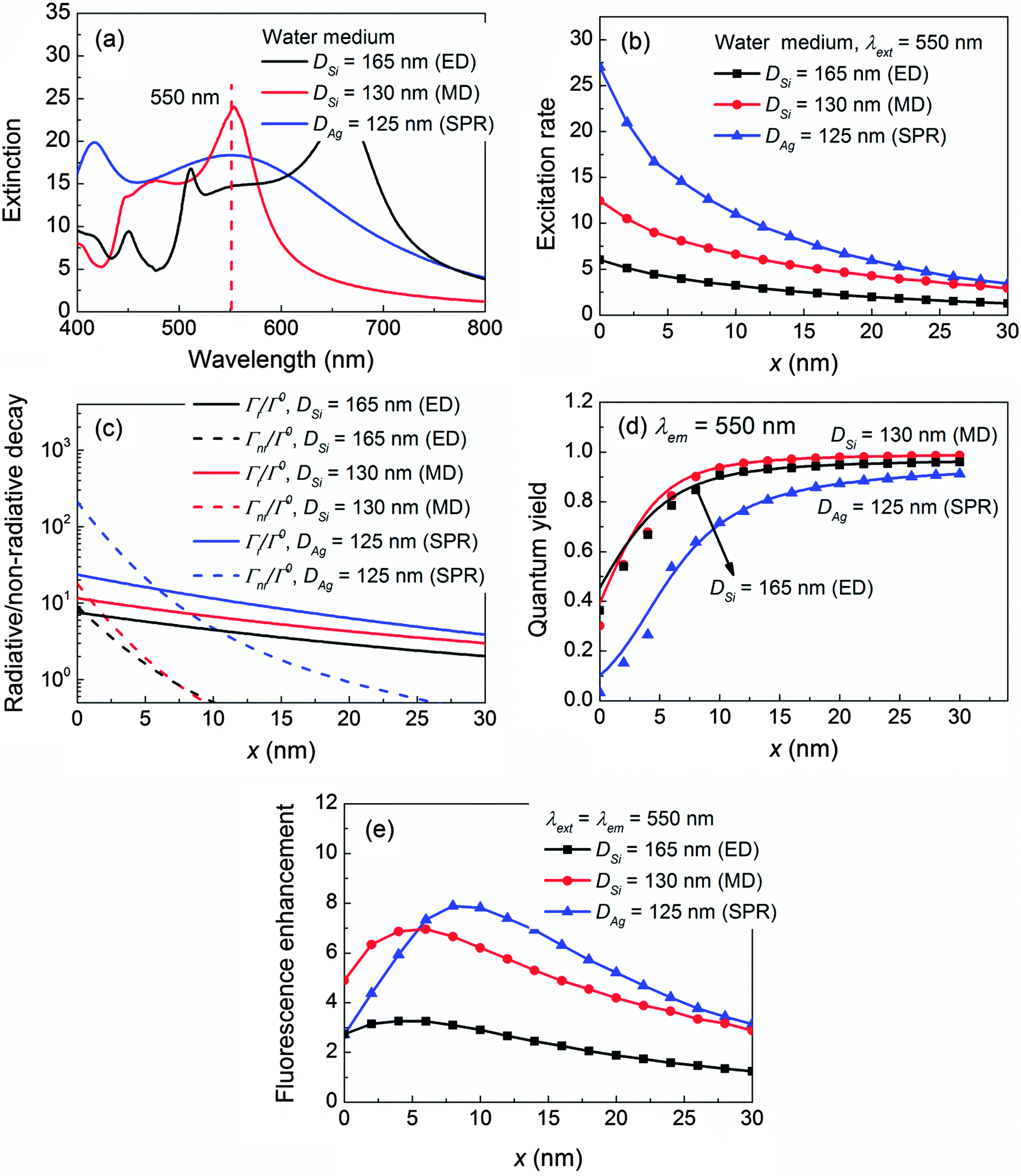 | ||
| Fig. 4 Fluorescence enhancement at 550 nm in the water medium. (a) The extinction spectrum of the NPs. The electric-dipole-mode (ED) of 165 nm Si, the magnetic-dipole-mode (MD) of 130 nm Si, and the plasmonic resonance (SPR) of 125 nm Ag are all located at a fluorescence excitation wavelength λext = 550 nm to ensure a fair comparison. (b) The NP-enhanced fluorescence excitation rate γext/γ0ext of the Si NP decreases tremendously in the water medium and is much smaller than that of the Ag NP. (c) The radiative decay rates Γr/Γ0 of the Si NP also decrease significantly in the water medium at the fluorescence emission wavelength λem = 550 nm. Γr/Γ0 of the Si ED drops 53.3% and that of Si MD drops 17%. (d) The quantum yield q/q0 of the Si NP is still higher than that of the Ag NP due to the low conductivity of Si at λem = 550 nm. However, it is not enough to compensate the decrement in the excitation rate. (e) The fluorescence enhancements ηem/η0em of the Si NP are weaker than those of the Ag NP in the water medium. | ||
Discussion
Fluorescence enhancements for fluorophores with large Stokes shifts
Up to now, we assume fluorophores have negligible Stokes shifts, e.g. λext = λem. In reality, some fluorescent dyes (e.g. Alexa 430, Fura Red etc.)54 and quantum dots3 have large Stokes shifts where λext and λem can be well-separated up to a few hundred nanometers. In such cases, the NPs are commonly designed so that their resonance modes are tuned to align with λext so as to enhance the excitation rate. Meanwhile, λem should fall at the low conductivity region of the NP material to generate a high quantum yield. For illustration purposes, we assume that λext = 445 nm which corresponds to the ED of 125 nm Si and the SPR of 130 nm Ag in air medium (Fig. 2a), and vary λem at 445 nm, 550 nm and 650 nm. Fig. 5a and b show the quantum yields q/q0 at various λem for the Si and Ag NPs respectively. Apparently, q/q0 is higher as long as λem locates at the low conductivity region of Si (e.g. λem = 550 nm and 650 nm). Moreover, q/q0 of the Si NP is larger than that of the Ag NP regardless of λem because the conductivity of Si is generally much smaller than that of Ag. The corresponding fluorescence enhancements ηem/η0em are shown in Fig. 5c for the Si NP and the Ag NP. Clearly, the Si NP can always produce a comparable or even larger fluorescence enhancement in the air medium as compared to the plasmonic NP regardless of the Stokes shift. In the water medium, however, the Si NP still cannot outperform the plasmonic NP due to the giant decrement on the fluorescence excitation rate regardless of the Stokes shift. Details are presented in Fig. S9 in the ESI.†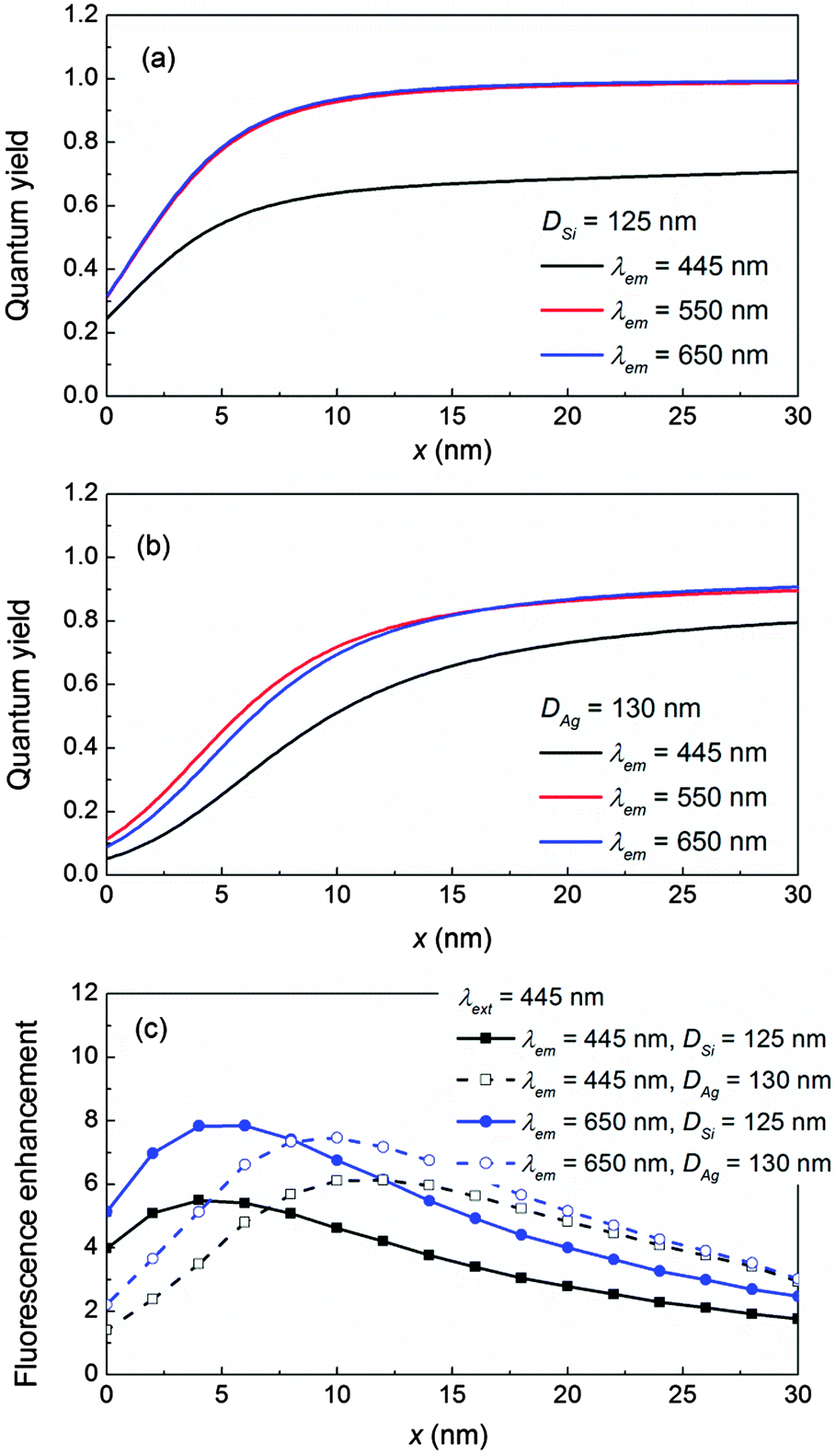 | ||
| Fig. 5 The effect of Stokes shift on the fluorescence enhancement. The quantum yield q/q0 for (a) 125 nm Si (ED = 445 nm) and (b) 130 nm Ag (SPR = 445 nm) at a fixed fluorescence excitation wavelength λext = 445 nm and various fluorescence emission wavelengths λem at 445 nm, 550 nm and 650 nm. q/q0 of the Si NP is generally larger than that of the Ag NP because the conductivity of Si is generally much smaller than that of Ag. (c) The respective fluorescence enhancements ηem/η0em for the Si NP (solid line with closed symbols) and the Ag NP (dashed line with open symbols). Regardless of the fluorescence Stokes shifts, the Si NP can always produce a comparable or even larger fluorescence enhancement in the air medium compared to the Ag NP. | ||
Far field intensity at the maximum fluorescence enhancement
Notice that the quantum yield q/q0 used in calculating the fluorescence enhancement ηem/η0em is a relative quantity to account for the competition between the radiative and non-radiative decay rates, which does not provide information on the absolute strength of fluorescence radiation (e.g. the far field intensity). For instance, q/q0 = 1 always holds true as long as the material conductivity is null, but the far field intensity still depends on the permittivity of the NP and the medium, as well as the fluorophore's location and wavelength. Therefore, complementary to the fluorescence enhancement ηem/η0em, the far field intensity also needs to be monitored as an indicator for the magnitude of fluorescence radiation. Fig. 6 records the far field intensities for the four cases studied previously in Fig. 2, 3, 4 and 5 respectively. The far field intensity is calculated with the fluorophore located at the optimal distance x where the maximum fluorescence enhancement is achieved (e.g. x = 4 nm, 6 nm and 12 nm for the Si ED, Si MD and Ag NP respectively for λext = λem = 445 nm in the air medium as in Fig. 6a).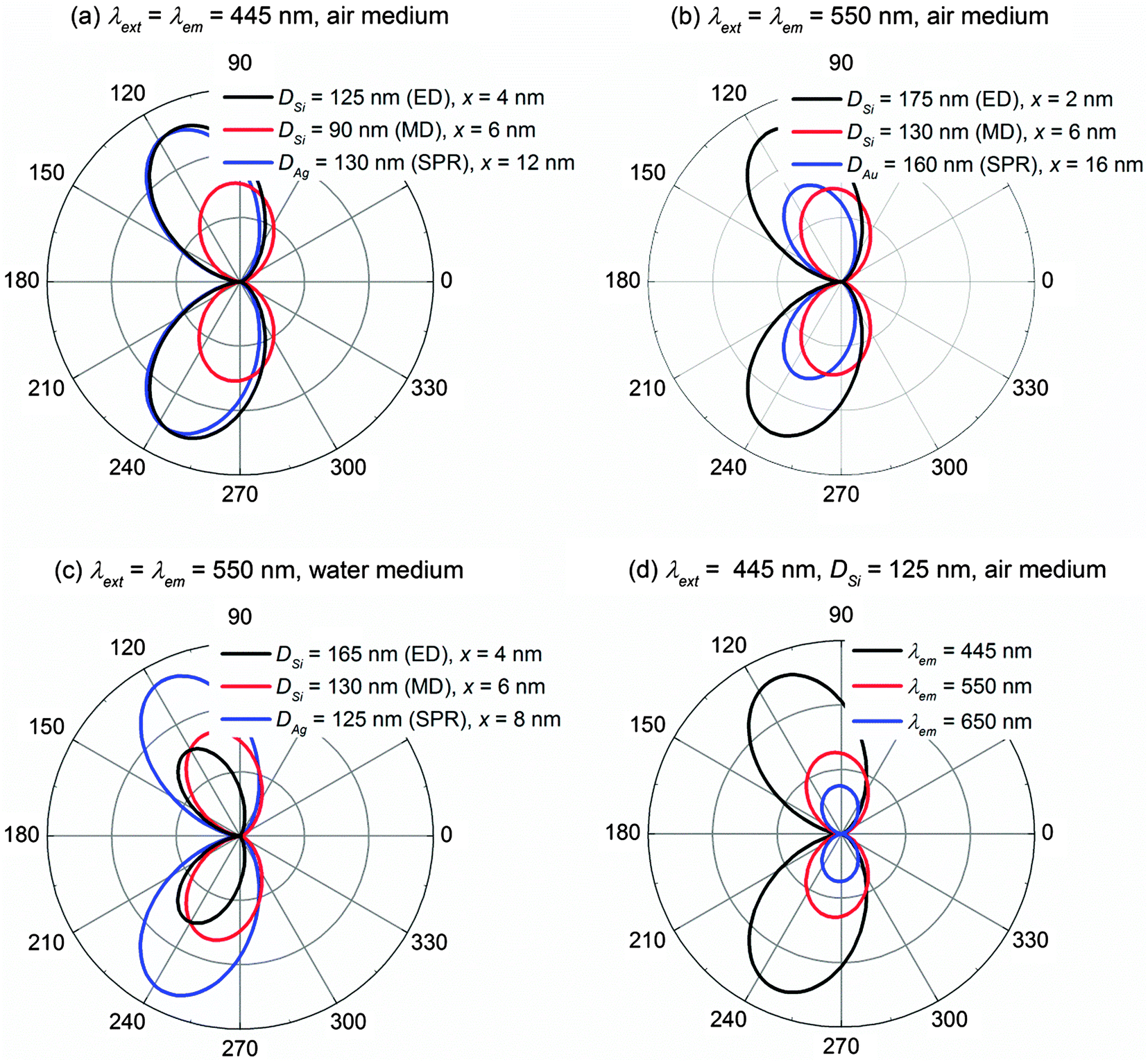 | ||
| Fig. 6 The far field intensities for fluorophore wavelengths at (a) λext = λem = 445 nm in the air medium, (b) λext = λem = 550 nm in the air medium, (c) λext = λem = 550 nm in the water medium and (d) λext = 445 nm and λem at 445 nm, 550 nm and 650 nm in the air medium. The far field intensity is taken at the optimal distance x where the maximum fluorescence enhancement is achieved. | ||
It is clear that in the air medium (Fig. 6a and b), the Si ED possesses a comparable or even higher far field intensity than those of the Si MD and the plasmonic NP because the Si ED can be strongly excited by an electric dipole. Details can be found in Fig. S1 in the ESI.† It is also noteworthy that the Si MD is able to generate a high fluorescence enhancement ηem/η0em (Fig. 2e and 3e) primarily due to the high quantum yield q/q0 resulting from the low conductivity nature of Si, but its far field intensity is much smaller than that of the Si ED. From this perspective, we find that the Si MD might not be as promising as the Si ED for fluorescence enhancement in the air medium since it cannot be strongly excited by the electric dipole.
In the water medium (Fig. 6c), the far field intensity of the Ag NP is much higher than those of both the Si ED and MD. The same conclusion has also been obtained for λext = λem = 650 nm in the water medium, whereby the far field intensity of the Au NP is much higher than those of the Si ED and MD. Details are shown in Fig. S8 in the ESI.† If fluorophores with large Stokes shifts are used, a longer emission wavelength λem leads to a smaller far field intensity because it is off-resonance of the Si ED (Fig. 6d). The same conclusion also applies to the plasmonic NP as the SPR behaves similarly to the dielectric ED. Details can be found in Fig. S10 in the ESI.†
Combining the results in Fig. 2, 3 and 6, we deduce that the optimum situation for the dielectric/plasmonic NP-enhanced fluorescence in the air medium appears when two conditions are satisfied: (1) the fluorescence excitation wavelength λext, fluorescence emission wavelength λem, and dielectric ED/plasmonic SPR are aligned at the same wavelength; (2) they fall at the low conductivity region of the NP material. As a result, both the fluorescence enhancement and far field intensity can be maximized simultaneously. If λext is not aligned with the ED/SPR, the fluorescence excitation rate cannot be maximized. If λem is off-resonance of the ED/SPR, the far field intensity will be compromised (Fig. 6d). Otherwise if the conductivity is high, large loss will be induced to spoil the quantum yields as well as the fluorescence enhancement (Fig. 2). Nevertheless, from a practical point of view, it is difficult to filter out the background incident light if λext = λem. In such cases, it is recommended to use fluorophores with Stokes shifts as small as possible.
Applicability of some commonly used dielectric materials for visible light fluorescence enhancement
To generate a large fluorescence enhancement, the ideal dielectric material should be loss-less and possess a permittivity as high as possible in order to produce a large fluorescence excitation rate. Fig. 7 illustrates a general guideline on the minimum permittivity requirement for an ideal loss-less (conductivity = 0) dielectric NP to outperform plasmonic counterparts in (a) the air medium for λext = λem = 445 nm, and (b) the water medium for λext = λem = 550 nm. The quantum yield is always q/q0 = 1 due to the absence of loss and the fluorescence enhancement ηem/η0em is exactly equal to the NP-enhanced excitation rate. The NP possesses a permittivity εNP while its size DNP is controlled so that the MD is consistent with the fluorescence excitation wavelength. The MD is chosen here since it always remains well-resolved in the extinction spectrum regardless of the medium and offers a comparable (in the air medium, Fig. 2b and 3b) or larger (in the water medium, Fig. 4b) excitation rate than the ED. In the air medium, a minimum εNP of 9 is identified to guarantee a higher ηem/η0em than that of the Ag NP as shown in Fig. 7a. In the water medium, it must be at least 16 to yield a higher ηem/η0em as shown in Fig. 7b. An even higher permittivity would be required than this minimum standard to outperform the plasmonic metal if the loss is presented in the dielectric material and the far field intensity is considered. Note that this general guideline serves an indicative purpose to roughly evaluate the potential of a particular dielectric material in the visible light fluorescence enhancement, and it also holds at other wavelengths. Details can be found in Fig. S11 in the ESI.†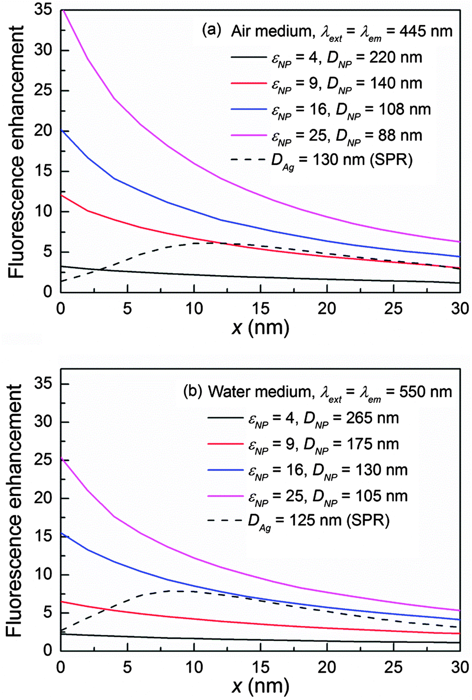 | ||
| Fig. 7 The general guideline on the minimum requirement on the permittivities εNP of an absolutely loss-less dielectric NP (conductivity = 0) to outperform the plasmonic NP in (a) the air medium for λext = λem = 445 nm and (b) the water medium for λext = λem = 550 nm. A minimum εNP of 9 is required to guarantee a higher fluorescence enhancement ηem/η0em than the Ag NP in the air medium, whereas it must be of 16 to outperform the Ag NP in the water medium. | ||
Based on the results in Fig. 7, in the air medium, Si is capable of producing a larger fluorescence enhancement than plasmonic metals because it possesses a much higher permittivity (14–30 in the visible light region) than the minimum requirement, which is sufficient to cover the loss. Other commonly used dielectric materials such as Ge, GaAs, and GaP, which also have large permittivities, could also be potentially applicable in the air medium. Among these materials, we believe Si is the best choice due to its relative large permittivity as well as its small conductivity (Si has a much smaller conductivity than Ge and GaAs) in the visible light region. Other than that, dielectric materials like TiO2, which has a moderate permittivity (7–8) and negligible loss in the visible light region is another potential candidate. Details on material properties can be found in Fig. S2 in the ESI.†
In the water medium, there is a higher requirement on the minimum permittivity so that dielectric materials like TiO2 are no longer applicable. In addition, although dielectric materials like Si, GaAs, and Ge etc. can fulfil the minimum permittivity requirement at certain wavelengths, they all suffer loss (Ge and GaAs in particular) in the visible light region, especially at violet-blue wavelengths (e.g. 400–500 nm). As a result, their fluorescence enhancements (Fig. 4) as well as far field intensities (Fig. 6c) can hardly beat those of the plasmonic NP. We speculate that the plasmonic metal currently is still a better choice for fluorescence enhancement in a high permittivity medium such as water or oil.
Other considerations for dielectric and plasmonic NPs
Besides the applicability and capability discussed above, there are two other considerations we wish to mention from a practical perspective.(1) The optimal distance is much shorter for the dielectric NP (e.g. x = 2–6 nm for Si) to achieve the maximum fluorescence enhancement compared to that of the plasmonic NP (e.g. x = 10–16 nm) due to the relatively low loss of the dielectric material. If the dielectric material is absolutely loss-less, the maximum fluorescence enhancement should occur exactly at the surface of the NP (Fig. 7). As a result, different lengths of linker molecules must be used for the dielectric and plasmonic NP to realize their respective maximum fluorescence enhancements in the multi-ligand approach.19
(2) Unlike the plasmonic NP, the dielectric NP possesses two resonance modes: the ED and MD, which naturally appear in the short and long wavelengths respectively. However, only the ED can be strongly excited by the routinely used fluorescent dyes and quantum dots,3,54 which in reality are electric dipoles by nature. So in general, it is not beneficial to utilize both modes (e.g. λext is aligned with the ED while λem is aligned with the MD) to enhance the fluorescence.
Conclusions
A systematic comparison has been conducted between high permittivity dielectrics and plasmonic metals on the fluorescence enhancements in the visible light regime based on nanoparticles (NPs), through the fluorescence excitation rate, quantum yield, fluorophore wavelengths and Stokes shifts, as well as far field intensities. In a low permittivity sensing medium (e.g. air), we found that a high permittivity (>9) dielectric NP is potentially able to generate a comparable or even higher fluorescence enhancement than the plasmonic NP such as a Ag or Au NP due to its decent NP-enhanced excitation rate and larger quantum yield. In a high permittivity sensing medium (e.g. water or oil), however, a giant decrement in the fluorescence excitation rate of the dielectric NP (especially its electric-dipole-mode (ED)) leads to a smaller fluorescence enhancement than that of the plasmonic NP. These conclusions hold true regardless of the fluorophore wavelengths and Stokes shifts. Selecting the fluorescence emission wavelength at the low conductivity region of the NP material (either dielectrics or plasmonic metals) can further improve the fluorescence enhancement by suppressing the non-radiative decay component. Furthermore, by monitoring the far field intensities, we pointed out that the optimal situation occurs when the fluorescence excitation wavelength, fluorescence emission wavelength and the ED of the dielectric NP (or the plasmonic resonance of the metal NP) are the same and all fall in the low conductivity region, thereby both the fluorescence enhancement and far field intensity can be maximized simultaneously. We also find that the ED of the dielectric NP performs better than the MD because only the ED can be strongly excited by the routinely used fluorescent dyes and quantum dots, although the MD may generate a high excitation rate. From a practical perspective, we notice that a much shorter linker molecule must be used in the experiment to realize the maximum fluorescence enhancement for the dielectric NP than that of the plasmonic NP, and the co-existence of the dielectric ED and MD might not be beneficial in fluorescence enhancement. Our results originate from the fundamental materials properties (e.g. permittivity and conductivity) and physics mechanisms, which can be extended to other nanostructures, offering a concrete guideline on fluorescence experiments in various situations.Methods
Calculation of fluorescence enhancement
The enhanced emission of a fluorescence emitter in the vicinity of a NP can be described based on the language of Förster resonance energy transfer (FRET),32,53 where the NP is viewed as a two-way antenna (both transmitter and receiver).12,29,37 Under this framework, the fluorescence enhancement of a single emitter ηem/η0em can be expressed as the product of the enhanced excitation rate γext/γ0ext and quantum yield q/q0 as shown in eqn (1),21,32,42 where the fluorophore is modelled as an oscillating electric dipole and the superscript 0 represents the corresponding quantity in a homogeneous medium. The excitation wavelength and emission wavelength of the fluorophore are denoted as λext and λem respectively.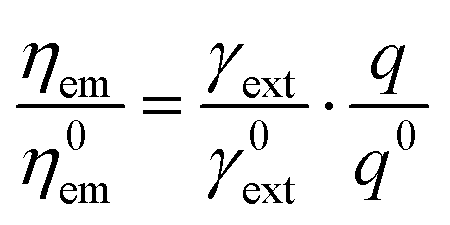 | (1) |
Below saturation, the excitation rate γext is proportional to |E·p|2, where E is the localized electric field at the location of the fluorescence and p is the dipole moment related to the orientation of the fluorophore. The quantum yield q is determined by the weighted sum of all possible decay channels within the validity of Fermi's golden rule as shown in eqn (2):
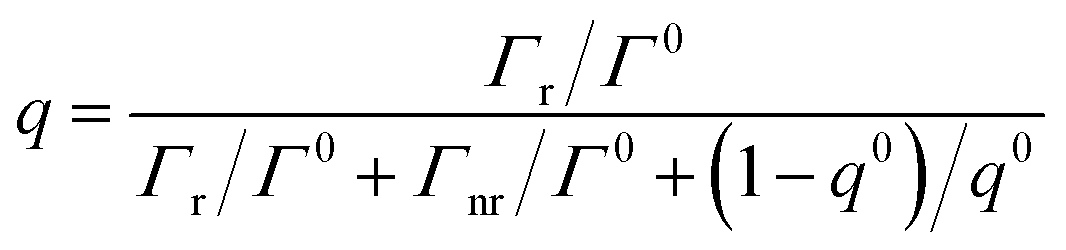 | (2) |
Determination of the radiative and non-radiative rate
A rigorous analytical solution for the enhancement in the radiative decay rate Γr/Γ0 and non-radiative decay rate Γnr/Γ0 has been developed for an electric dipole emitter near a spherical NP.51,52 In general, the electromagnetic field emitted from a dipole is expanded into a series of spherical harmonics, and the interaction between the NP and each harmonic is governed by the Mie theory. In this paper, we follow Ruppin's formulisms,51 while alternative forms are also available.42,52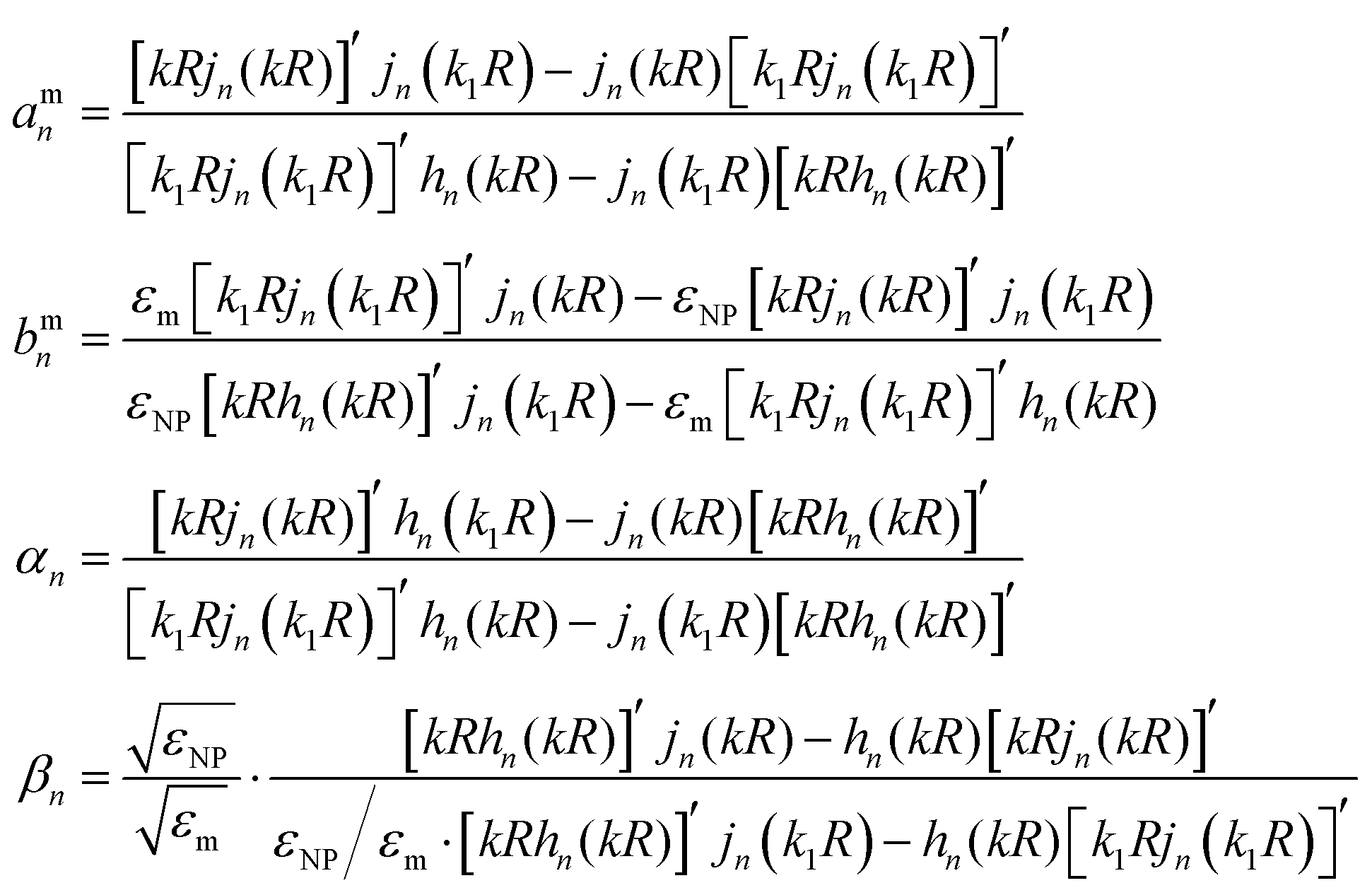 | (3) |
The radiative decay rate is determined through computing the Poynting vector and integrating the power flux over the surface of a large sphere in the far field domain, whereas the non-radiative decay takes into account the ohmic loss inside the NP. We consider the following two fluorophore orientations: perpendicular (superscript ⊥) and parallel (superscript ‖) to the surface of the NP, while other orientations can always be decomposed into these two cases. The corresponding decay rates are:
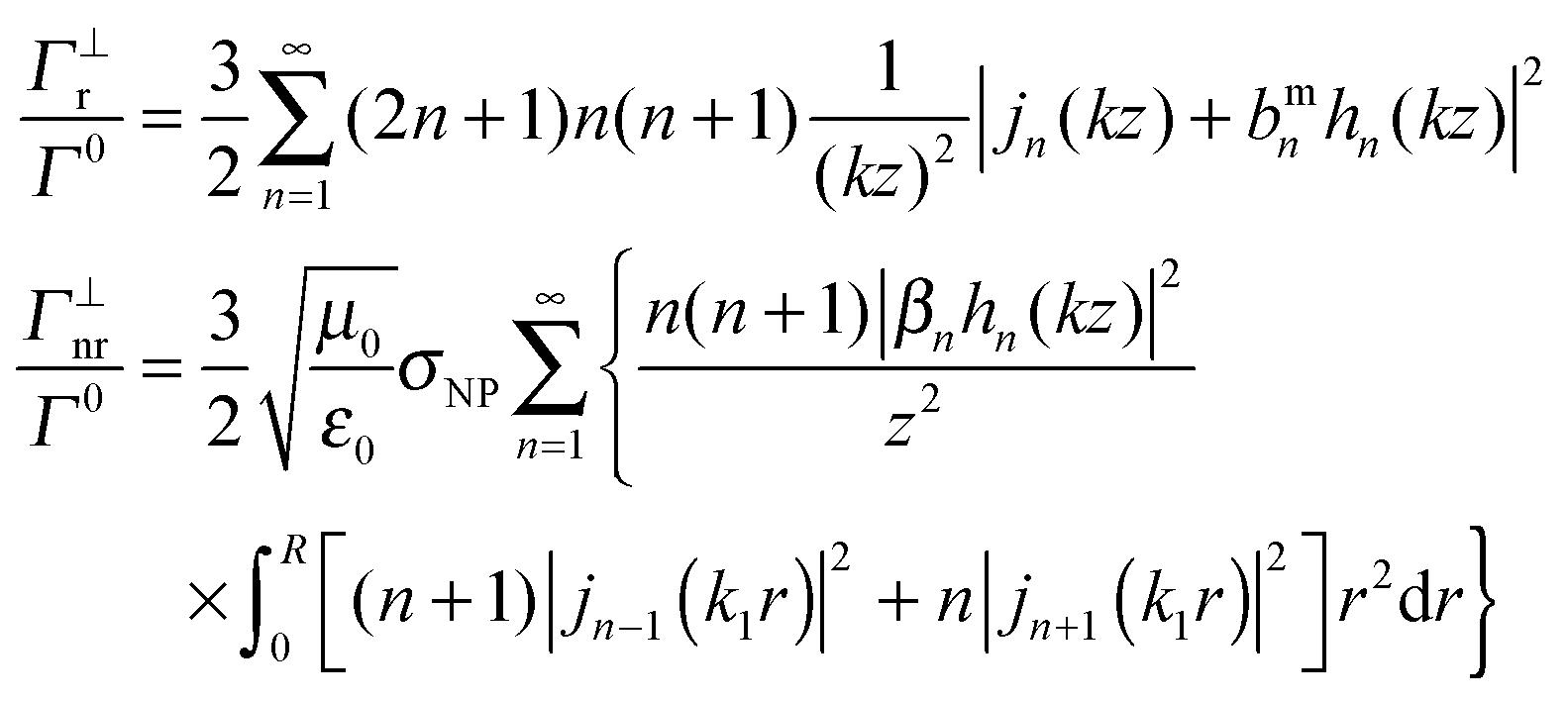 | (4) |
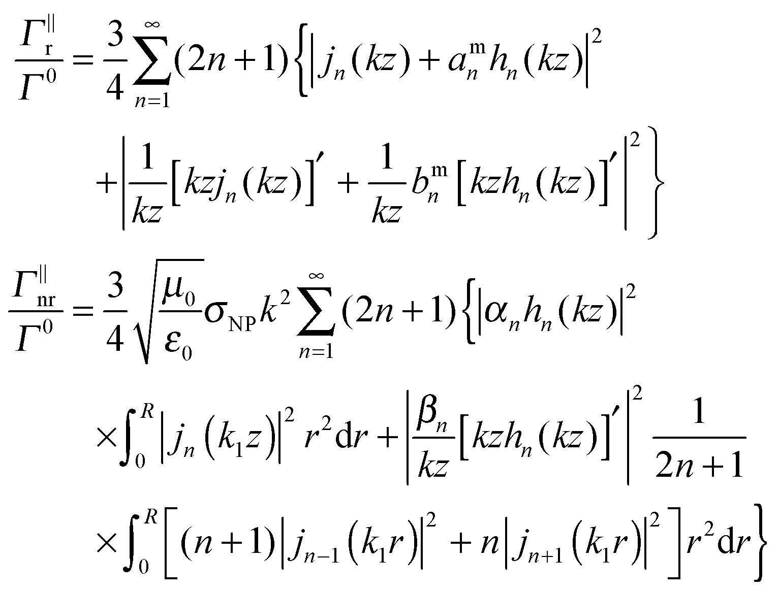 | (5) |
Finite element method (FEM)
To ensure correctness, the above analytical solution is verified with the numerical method FEM using the commercial software COMSOL Multiphysics. The scattered wave formulation has been adopted. The radiative (non-radiative) decay rate is obtained as Γr/Γ0 = Psca/P0 (Γnr/Γ0 = Pabs/P0), where Psca represents the scattered power collected in the far field domain, Pabs is the power absorbed by the NP and P0 is the power radiated by an identical dipole in the homogeneous medium.21 The near field enhancement of the NP is also obtained using the FEM.Acknowledgements
This work is supported by Agency for Science, Technology and Research, PHAROS grant (A*STAR-SERC Grant No. 152-73-00025).References
- G. Gauglitz, Annu. Rev. Anal. Chem., 2014, 7, 297–315 CrossRef CAS PubMed.
- J. Homola, Chem. Rev., 2008, 108, 462–493 CrossRef CAS PubMed.
- U. Resch-Genger, M. Grabolle, S. Cavaliere-Jaricot, R. Nitschke and T. Nann, Nat. Methods, 2008, 5, 763–775 CrossRef CAS PubMed.
- H. P. Lu, L. Y. Xun and S. Xie, Science, 1998, 282, 1877–1882 CrossRef CAS PubMed.
- S. Uemura, C. E. Aitken, J. Korlach, B. A. Flusberg, S. W. Turner and J. D. Puglisi, Nature, 2010, 464, 1012–1017 CrossRef CAS PubMed.
- J. Malicka, I. Gryczynski, Z. Gryczynski and J. R. Lakowicz, Anal. Chem., 2003, 75, 6629–6633 CrossRef CAS PubMed.
- C. Eggeling, C. Ringemann, R. Medda, G. Schwarzmann, K. Scandoff, S. Polyakova, V. N. Belov, B. Hein, C. V. Middendorff, A. Schönle and S. W. Hell, Nature, 2009, 457, 1159–1162 CrossRef CAS PubMed.
- T. D. Mang, C. McGinnis, C. Liebow, U. O. Nseyo, D. H. Crean and T. J. Dougherty, Cancer, 1993, 71, 269–276 CrossRef CAS PubMed.
- M. Smilkstein, N. Sriwilaijaroen, J. X. Kelly, P. Wilairat and M. Riscoe, Antimicrob. Agents Chemother., 2004, 48, 1803–1806 CrossRef CAS PubMed.
- E. Sikorska, T. Górecki, I. V. Khmelinskii, M. Sikorski and J. Koziol, Food Chem., 2005, 89, 217–225 CrossRef CAS.
- W. L. Barnes, A. Dereux and T. W. Ebbesen, Nature, 2003, 424, 824–830 CrossRef CAS PubMed.
- L. Novotny and N. V. Hulst, Nat. Photonics, 2011, 5, 83–90 CrossRef CAS.
- M. Bauch, K. Toma, M. Toma, Q. W. Zhang and J. Dostalek, Plasmonics, 2014, 9, 781–799 CrossRef CAS PubMed.
- S. Kühn, U. Håkanson, L. Rogobete and V. Sandoghdar, Phys. Rev. Lett., 2006, 97, 017402 CrossRef PubMed.
- K. A. Willets and R. P. Van Duyne, Annu. Rev. Phys. Chem., 2007, 58, 267–297 CrossRef CAS PubMed.
- T. Ozel, S. Nizamoglu, M. A. Sefunc, O. Samarskaya, I. O. Ozel, E. Mutlugun, V. Lesnyak, N. Gaponik, A. Eychmuller, S. V. Gaponenko and H. V. Demir, ACS Nano, 2011, 5, 1328–1334 CrossRef CAS PubMed.
- H. Aouani, O. Mahboub, N. Bonod, E. Devaux, E. Popov, H. Rigneault, T. W. Ebbesen and J. Wenger, Nano Lett., 2011, 11, 637–644 CrossRef CAS PubMed.
- Z. Xi, Y. H. Lu, P. J. Yao, W. H. Yu, P. Wang and H. Ming, Opt. Express, 2013, 21, 30327–30335 Search PubMed.
- P. Sharma, S. Brown, G. Walter, S. Santra and B. Moudgil, Adv. Colloid Interface Sci., 2006, 123–126, 471–485 CrossRef CAS PubMed.
- D. Punj, M. Mivelle, S. B. Moparthi, T. S. V. Zanten, H. Rigneault, N. F. V. Hulst, M. F. García-Parajó and J. Wenger, Nat. Nanotechnol., 2013, 8, 512–516 CrossRef CAS PubMed.
- M. Bauch and J. Dostalek, Opt. Express, 2013, 21, 20470–20483 CrossRef PubMed.
- P. P. Pompa, L. Martiradonna, A. D. Torre, F. D. Sala, L. Manna, M. D. Vittorio, F. Calabi, R. Cingolani and R. RinaldI, Nat. Nanotechnol., 2006, 1, 126–130 CrossRef CAS PubMed.
- H. F. Yuan, S. Khatua, P. Zijlstra, M. Yorulmaz and M. Orrit, Angew. Chem., Int. Ed., 2013, 52, 1217–1221 CrossRef CAS PubMed.
- K. Ray, R. Badugu and J. R. Lakowicz, J. Am. Chem. Soc., 2006, 128, 8998–8999 CrossRef CAS PubMed.
- T. H. Taminiau, F. D. Stefani, F. B. Segerink and N. F. V. Hulst, Nat. Photonics, 2008, 2, 234–237 CrossRef CAS.
- H. Aouani, O. Mahboub, E. Devaux, H. Rigneault, T. W. Ebbesen and J. Wenger, Nano Lett., 2011, 11, 2400–2406 CrossRef CAS PubMed.
- M. H. Chowdhury, J. Pond, S. K. Gray and J. R. Lakowicz, J. Phys. Chem. C, 2008, 112, 11236–11249 CAS.
- H. Cang, Y. M. Liu, Y. Wang, X. B. Yin and X. Zhang, Nano Lett., 2013, 13, 5949–5953 CrossRef CAS PubMed.
- P. Anger, P. Bharadwaj and L. Novotny, Phys. Rev. Lett., 2006, 96, 113002 CrossRef PubMed.
- E. Dulkeith, A. C. Morteani, T. Niedereichholz, T. A. Klar and J. Feldmann, Phys. Rev. Lett., 2002, 89, 203002 CrossRef CAS PubMed.
- T. L. Jennings, M. P. Singh and G. F. Strouse, J. Am. Chem. Soc., 2006, 128, 5462–5467 CrossRef CAS PubMed.
- P. Andrew and W. L. Barnes, Science, 2000, 290, 785–788 CrossRef CAS PubMed.
- X. C. Ma, Y. Dai, L. Yu and B. B. Huang, Light: Sci. Appl., 2016, 5, e16017 CrossRef CAS.
- Z. Y. Wang, Y. Y. Liu, B. B. Huang, Y. Dai, Z. Z. Lou, G. Wang, X. Y. Zhang and X. Y. Qin, Phys. Chem. Chem. Phys., 2014, 16, 2758–2774 RSC.
- X. Zhang, C. A. Maricico, M. Lunz, V. A. Gerard, Y. K. Gun'ko, L. Vladimir, N. Gaponik, A. S. Sush, A. L. Rogach and A. L. Bradley, ACS Nano, 2014, 8, 1273–1283 CrossRef CAS PubMed.
- J. R. Lakowicz, Anal. Biochem., 2005, 337, 171–194 CrossRef CAS PubMed.
- P. Bharadwaj and L. Novotny, Opt. Express, 2007, 15, 14266–14274 CrossRef CAS PubMed.
- C. S. Yun, A. Javier, T. Jennings, M. Fisher, S. Hira, S. Peterson, B. Hopkins, N. O. Reich and G. F. Strouse, J. Am. Chem. Soc., 2005, 127, 3115–3119 CrossRef CAS PubMed.
- A. E. Krasnok, A. E. Miroshnichenko, P. A. Belov and Y. S. Kivshar, Opt. Express, 2012, 20, 20599–20604 CrossRef PubMed.
- B. Rolly, B. Stout and N. Bonod, Opt. Express, 2012, 20, 20376–20386 CrossRef PubMed.
- J. Van de Groep and A. Polman, Opt. Express, 2013, 21, 26285–26302 CrossRef CAS PubMed.
- M. K. Schmidt, R. Esteban, J. J. Sáenz, I. Suárez-Lacalle, S. Mackowski and J. Aizpurua, Opt. Express, 2012, 20, 13636–13650 CrossRef CAS PubMed.
- Y. H. Fu, A. I. Kunznetsov, A. E. Miroshnichenko, Y. F. Yu and B. Luk'yanchuk, Nat. Commun., 2013, 4, 1527 CrossRef PubMed.
- P. Albella, M. A. Poyli, M. K. Schmidt, S. A. Maier, F. Moreno, J. J. Sáenz and J. Aizpurua, J. Phys. Chem. C, 2013, 117, 13573–13584 CAS.
- A. I. Kuznetsov, A. E. Miroshnichenko, Y. H. Fu, J. B. Zhang and B. Luk'yanchul, Sci. Rep., 2012, 2, 492 Search PubMed.
- M. Caldarola, P. Albella, E. Cortés, M. Rahmani, T. Roschuk, G. Grinblat, R. F. Oulton, A. V. Bragas and S. A. Maier, Nat. Commun., 2015, 6, 7915 CrossRef CAS PubMed.
- S. Person, M. Jain, Z. Lapin, J. J. Sáenz, G. Wicks and L. Novotny, Nano Lett., 2013, 13, 1806–1809 CrossRef CAS PubMed.
- P. Albella, R. A. De la Osa, F. Moreno and S. A. Maier, ACS Photonics, 2014, 1, 524–529 CrossRef CAS.
- C. T. Cheng, C. X. Wang, Q. Kan, B. J. Huang, Z. Z. Wang, H. S. Gao and H. D. Chen, J. Lightwave Technol., 2014, 32, 461–466 CrossRef CAS.
- G. Pellegrini, G. Mattei and P. Mazzoldi, ACS Nano, 2009, 3, 2715–2721 CrossRef CAS PubMed.
- R. Ruppin, J. Chem. Phys., 1982, 76, 1681–1684 CrossRef CAS.
- V. V. Klimov and V. S. Letokhov, Laser Phys., 2005, 15, 61–73 CAS.
- E. D. Palik, Handbook of Optical Constants of Solid, Academic press, New York, 1985, vol. 1, pp. 286-295 (Au), pp. 350–351 (Ag), pp. 547–552 (Si) Search PubMed.
- http://www.leica-microsystems.com/science-lab/fluorescent-dyes/ .
- C. Ayala-Orozco, J. G. Liu, M. W. Knight, Y. M. Wang, J. K. Day, P. Nordlander and N. J. Halas, Nano Lett., 2014, 14, 2926–2933 CrossRef CAS PubMed.
- K. Toma, M. Vala, P. Adam, J. Homola, W. Knoll and J. Dostálek, Opt. Express, 2013, 21, 10121–10132 CrossRef CAS PubMed.
- C. J. Huang, J. Dostalek, A. Sessitsch and W. Knoll, Anal. Chem., 2011, 83, 674–677 CrossRef CAS PubMed.
- A. García-Etxarri, R. Gómez-Medina, L. S Froufe-Pérez, C. López, L. Chantada, F. Scheffold, J. Aizpurua, M. Nieto-Vesperinas and J. J. Sáenz, Opt. Express, 2011, 19, 4815–4826 Search PubMed.
Footnote |
| † Electronic supplementary information (ESI) available: Detailed mode composition, mode excitation by electric dipole, material properties of commonly used dielectrics, decay rate and quantum yield excited by a parallel dipole, quantum yield enhancement at low conductivity of plasmonic nanoparticles, change in the extinction spectrum of Si nanoparticles at various medium permittivities, fluorescence enhancement in water medium at 650 nm, fluorescence with large Stokes shifts in water medium, far field intensity of plasmonic NPs. See DOI: 10.1039/c6cp03303b |
| This journal is © the Owner Societies 2016 |