
 Open Access Article
 This Open Access Article is licensed under a Creative Commons Attribution-Non Commercial 3.0 Unported Licence
High-performance colossal permittivity materials of (Nb + Er) co-doped TiO2 for large capacitors and high-energy-density storage devices†
Mei-Yan
Tse
a,
Xianhua
Wei
ab and
Jianhua
Hao
*a
aDepartment of Applied Physics, The Hong Kong Polytechnic University, Hung Hom, Hong Kong, P. R. China. E-mail: jh.hao@polyu.edu.hk; Fax: +852 23337629; Tel: +852 27664098
bState Key Laboratory Cultivation Base for Nonmetal Composites and Functional Materials, Southwest University of Science and Technology, Mianyang 621010, P. R. China
First published on 2nd August 2016
Abstract
The search for colossal permittivity (CP) materials is imperative because of their potential for promising applications in the areas of device miniaturization and energy storage. High-performance CP materials require high dielectric permittivity, low dielectric loss and relatively weak dependence of frequency- and temperature. In this work, we first investigate the CP behavior of rutile TiO2 ceramics co-doped with niobium and erbium, i.e., (Er0.5Nb0.5)xTi1−xO2. Excellent dielectric properties were observed in the materials, including a CP of up to 104–105 and a low dielectric loss (tan![[thin space (1/6-em)]](https://www.rsc.org/images/entities/char_2009.gif) δ) down to 0.03, which are lower than that of the previously reported co-doped TiO2 CP materials when measured at 1 kHz. Stabilities of frequency and temperature were also accomplished via doping Er and Nb. Valence states of the elements in the material were analyzed using X-ray photoelectron spectroscopy. The Er induced secondary phases were observed using elemental mapping and energy-dispersive spectrometry. Consequently, this work may provide comprehensive guidance to develop high-performance CP materials for fully solid-state capacitor and energy storage applications.
δ) down to 0.03, which are lower than that of the previously reported co-doped TiO2 CP materials when measured at 1 kHz. Stabilities of frequency and temperature were also accomplished via doping Er and Nb. Valence states of the elements in the material were analyzed using X-ray photoelectron spectroscopy. The Er induced secondary phases were observed using elemental mapping and energy-dispersive spectrometry. Consequently, this work may provide comprehensive guidance to develop high-performance CP materials for fully solid-state capacitor and energy storage applications.
1. Introduction
With an ever increasing demand for clean and sustainable energy, much effort has been put into developing new dielectric materials with high-energy-density storage. In this regard, suitable dielectric based solid-state capacitors with a high CP (>103) and a low dielectric loss (<10−1) play a vital role in miniaturization of electronic and energy storage devices.1–3 In order to achieve high-performance for practical applications, the designed dielectric materials should also satisfy nearly temperature- and frequency-independent dielectric constants (εr) and small dielectric loss (tanδ).4–6
Currently, a wide range of solid-state capacitors with CP have been developed but maximizing their performance by fulfilling all the aforementioned requirements remains a barrier. This is because most of the approaches would improve one dielectric parameter but simultaneously degrade the others.7 For instance, the typical ferroelectric materials, BaTiO3-based perovskites, can only attain CP at the tetragonal-cubic phase transition temperature (Tc ∼ 120 °C).8 The strong temperature dependence of the ferroelectric materials limits their applications to the devices working in a wide temperature range. The non-ferroelectric material CaCu3Ti4O12 (CCTO) exhibits giant permittivity values.9 Unfortunately, the mechanism of CP existing in CCTO is now unclear in terms of an internal barrier layer capacitor (IBLC) structure of thin insulating grain boundaries and conducting grain interior regions. Although high temperature-independent permittivity (∼105) can be achieved, tanδ of CCTO is relatively high (>10−1).
Recently, (In + Nb) co-doped titanium oxide (TiO2) exhibiting large temperature and frequency independence CP (>104) as well as a low dielectric loss (<0.05) has been reported by Liu's group.10,11 Its superior dielectric properties can be explained by the electron-pinned defect-dipole, in which hopping electrons are localized. Doping of extrinsic trivalent ions, and other cations in equivalent stoichiometric proportion has also been presented.12,13 There is an ongoing need for further research to design high-performance CP material systems using appropriate acceptor–donor co-doping.
Titanium oxide is one of the most important candidates for photocatalysts, solar cells, sensors, transparent conducting oxide (TCO) films and for energy conversion and storage applications.14 It has been shown that Nb doping would enhance the performance in energy conversion and storage applications.15
TiO2 exhibits three polymorphs, which are rutile, anatase, and brookite.16 In this work, rutile-type TiO2 with a P42/mnm, tetragonal structure was chosen as the parent oxide. Being a dielectric material, it combines both the satisfactory dielectric constant (>100)17 and a high dielectric breakdown strength (BDS > 100 kV cm−1),18 which are two important parameters to fabricate capacitors with a high energy density. Therefore, doped TiO2 materials with CP would be a highly attractive proposition. Here enhanced εr, low tanδ, less frequency- and temperature-dependence are firstly achieved in (Er0.5Nb0.5)xTi1−xO2 ceramics, in which Er3+ acts as the electron acceptor while Nb5+ is the substitution donor. The distribution of defects and solutes at grain boundaries may influence many properties of polycrystalline materials but few studies have been conducted on this group of CP materials. Besides, the general relationship between larger ionic radii of the acceptor ion and the presence or the absence of a defect dipole effect remains unknown. Er3+ with a larger ionic radius, (0.745 Å) < (0.94 Å) < (1.03 Å), was used. It is expected that this difference may affect the formation of defect dipole clusters as well as the overall dielectric properties. The presence of secondary phases at the grain boundary was also observed. A large εr (∼8.6 × 10⁴) and sufficiently low tanδ (4%) were simultaneously observed in the 5 mol% (Nb + Er)-modified TiO2 ceramics. Synthesis optimization, structural analysis, characterization of the dielectric properties and energy storage density are systematically investigated in the materials. This novel high-performance CP ceramics may be attractive for potential fully solid-state capacitor and high-energy-density storage applications.
2. Experimental procedure
Samples of (Er0.5Nb0.5)xTi1−xO2 were prepared using the solid state sintering method. Raw materials used in this work were rutile TiO2 (99.90%, Sigma-Aldrich), Nb2O5 (99.99%, Sigma-Aldrich) and Er2O3 (99.5%). These powders were weighed accurately according to their chemical compositions. The mixing and grinding processes were carried out by ball-milling using zirconia balls for 8 h in ethanol. All of the mixed powders were calcined at 970 °C for 4 h in air. The calcined powders incorporating polyvinyl alcohol (PVA) binder solution were pressed into disks with a diameter of around 12 mm and a thickness of 1.0 mm. Disk samples were then sintered at 800 °C for 2 h in air for burning out all the PVA binder. The samples were sintered at their optimal temperature of 1200–1500 °C for 10 h to obtain the dielectric properties. The sintered samples were pasted with silver on both sides and annealed at 750 °C for 30 min in air.The phase structures were confirmed by X-ray diffraction (XRD) with Cu Kα (λ = 0.154 nm) radiation (Smart Lab; Rigaku Co., Japan) and Raman spectroscopy (Jobin-Yvon Horiba HR800, France). Thermogravimetric Analysis (TGA) and Differential Scanning Calorimetry (DSC) were employed to analyze thermal behavior of the calcined powder. Scanning electron microscopy (SEM, JSM-6490, JEOL Ltd, Japan) was used to examine the surface morphologies, energy-dispersive spectrometry (EDS) and elemental mapping of the sintered samples. X-ray photoelectron spectroscopy (XPS) analysis was conducted on the system of a Sengyang SKL-12 electron spectrometer equipped with a VG CLAM 4MCD electron energy analyzer for analyzing valence states of elements in the materials. For the dielectric measurements at a high temperature (298–750 K), the samples were connected to the impedance analyzer inside a Carbolite furnace. A cryostat was used to characterize low temperature dependencies of dielectric parameters in the range of 80–296 K. An impedance analyzer (HP 4294A; Agilent Technologies Inc., Palo Alto, CA) was used to measure the frequency dependence of the dielectric properties over the range of 102 to 105 Hz.
3. Results and discussion
Fig. 1(a) and (b) show the XRD patterns of the sintered (Nb + Er) co-doped TiO2 ceramics at different doping levels in the 2θ range of 20° to 75°. The results suggest that the samples are of the rutile phase. There was a small shift towards a low diffraction angle, which was ascribed to the doping of Er3+ and Nb5+ ions into the TiO2 host lattice, resulting in an increased lattice strain. A small amount of secondary phases, Er2O3 (JCPDS #26-0604) and Er2Ti2O7 (JCPDS #18-0499), was seen in the ceramics, particularly when the concentration of Er3+ was greater than 2.5%. In tetragonal rutile crystals, Ti4+ (radius 0.745 Å) associated with six O2− (radius 1.26 Å) forms a [TiO6] octahedron.19 Dopants Er3+ (radius 1.03 Å) and Nb5+ (radius 0.78 Å)19 replace Ti4+ in a lattice to form [ErO6] and [NbO6] octahedrons, respectively, for maintaining the charge neutrality. Due to a similar ionic size to Ti4+, it is believed that Nb5+ would preferentially undergo the substitution at the Ti4+ sites; whist the large Er3+ ions might thus become “excessive” and result in the secondary phase formation. This finding demonstrates that only a small amount of Er3+ could be easily doped into the Ti4+ sites and the excess Er3+ would contribute to the secondary phase. In addition, a pure rutile phase was observed for the ceramics doped with only 0.5% Nb, as shown in Fig. 1(b). | ||
| Fig. 1 XRD patterns of (Er0.5Nb0.5)xTi1−xO2 sintered ceramics: (a) x = 0.25%, 0.5%, 1%, 2.5%, 7.5% and 10%, (b) x = 0%, 0.5% only Nb and 0.5% only Er. | ||
Fig. 2(a) and (b) present Raman spectra of the sintered (Nb + Er) co-doped TiO2 ceramics at different doping levels under excitation with a 488 nm Ar+ laser at room temperature. There are four Raman active fundamental modes in pure rutile TiO2: B1g (143 cm−1), Eg (447 cm−1), A1g (612 cm−1), and B2g (826 cm−1), which are similar to the previous results.12 B1g corresponds to the O–Ti–O bond bending mode, A1g corresponds to the Ti–O stretch mode while the Eg mode is due to oxygen atom liberation along the c-axis out of phase.12 It should be noted that the peak at around 240 cm−1 was a multi-phonon peak for the second-order effect (SOE).20 It is generally believed that this peak was caused by the internal stress/strain and partial reduction of the TiO2 grains. The result confirmed the incorporation of Nb5+ and Er3+ into the lattice of TiO2. However, there was a slight shift for Eg and A1g in the ceramics, which might arise from the lattice deformation caused by using elements with different radii.21 Raman spectroscopy analysis was in accord with the XRD phase evaluations. It was observed that only the ceramics doped at a low amount of Er3+ had a pure rutile phase; otherwise, secondary phases might appear. It is worth-noting that all the ceramics showed a rutile phase even if some secondary phases were formed.
 | ||
| Fig. 2 Raman spectra: (a) TiO2 ceramics doped with various contents of Er and Nb, (b) pure TiO2 ceramics. | ||
In order to clarify the morphological evolutions and elemental distributions of ceramic samples, their SEM images, elemental mapping and EDS were obtained. All of the characterized ceramics were clearly observed to have a dense microstructure, as shown in Fig. 3(a)–(h). An average grain size (∼3.5 μm) was observed for a pure TiO2 ceramic, grain sizes were increased at x = 0.25% (Fig. 3(b)) and then gradually decreased with increasing content (at values of x ≥ 1%), as shown in Fig. 3(b)–(f). There are two microstructure regions that differ in the grain size and phase composition. Besides, the distribution of non-homogeneous phase composition increased with x. According to the results of XRD patterns, the secondary phases were generated in the ceramics with x > 0.25%. It implies that the decreased grain sizes could be ascribed to the existence of secondary phases. The ceramic with x = 5% (Fig. 3(e)) had a denser structure and a smaller grain size distribution, giving rise to its high permittivity performance in the subsequent dielectric properties.
 | ||
| Fig. 3 Surface morphologies of the (Er0.5Nb0.5)xTi1−xO2 ceramics with different doping contents: (a) x = 0%, (b) x = 0.25%, (c) x = 1%, (d) x = 2.5%, (e) x = 5%, (f) x = 7.5%, (g) 0.5% only Nb and (h) 0.5% only Er; the insets in (a), (g) and (h) are the magnifications of the SEM images of the ceramics. | ||
To clearly reveal the grain-size evolution, the surface images of 0.5% Nb or Er singly-doped TiO2 ceramics are shown in Fig. 3(g) and (h), respectively. Nb5+ and Er3+ at lower concentrations enhanced grain growth while they inhibited grain growth at levels close to or above the dopant solubility with respect to pure TiO2 ceramics. It was proposed that Er3+ predominantly (about 90%) located in the interstitial position.22,23 The observations imply that the extra Er3+ may easily locate at the grain boundaries, which is an important approach for the inhibition of grain boundary mobility, resulting in the reduced grain sizes.
To characterize the distributions of Nb5+ and Er3+ in the TiO2 matrix and further explore the formation mechanisms of secondary phases, elemental mapping and EDS were performed as shown in Fig. 4(a)–(c). The results indicate that only Nb5+ were homogeneously distributed throughout the ceramics, regardless of the grain size. There were regions obviously rich in Er3+ associated with non-homogeneous grains (indicated by the blue spot). This observation is similar to CCTO, where Cu2+ segregation was reported.24 In addition, grain boundary segregation behaviour is presented in several dopants (Ca,25 Mn,18 Zn26 and Y27) of TiO2 ceramics. It is then suggested that the segregation of Er3+ is likely to occur towards the grain boundary areas. Such segregation may intensify at higher content x, as shown in Fig. 4(a)–(c). The result confirms that there is considerably higher Er3+containing secondary phases owing to ionic radius misfit of Ti4+.
 | ||
| Fig. 4 Element mapping and EDS of the ceramics across entire section with (a) x = 0.25%, (b) x = 2.5% and (c) x = 7.5%. | ||
Fig. 5(a) and (b) show the dielectric properties of the ceramics at different dopant contents x, measured at 1 kHz and room temperature. For pure TiO2, a relatively low εr (∼800) with tanδ (∼2%) was observed. The value of εr was significantly enhanced initially and then steadily increased with x. Besides, their corresponding tanδ fluctuated as x changed. An excellent dielectric behavior was achieved in the ceramics with x = 5%, where εr and tanδ are ∼8.6 × 10⁴ and 4%, respectively. More importantly, lower tanδ would be found in most ceramics, which were superior to the reported standard model in (Nb + In) or (Nb + Bi)-modified TiO2 ceramics.12,28 The results from SEM illustrate that both CP and low tanδ could be accomplished regardless of the aggregation of Er3+ at the grain boundaries, differing from the previous findings where the dopants were homogeneously distributed across the grains and grain boundaries.10–13 Otherwise, a severe deterioration in the dielectric loss might be resulted. Therefore, it is suggested that low tanδ achieved in the (Nb + Er)-modified TiO2 ceramics was possibly related to the formation of secondary phases.
 | ||
| Fig. 5 Dielectric properties: (a) (Er0.5Nb0.5)xTi1−xO2 ceramics as a function of doped content x, (b) doped 0.5% only Nb, 0.5% only Er and 0.5% (Nb + Er) co-doped TiO2 ceramics, measured at 1 kHz and room temperature. | ||
In order to familiarize the grounds for the enhanced dielectric behaviors, Fig. 5(b) shows that the ceramics co-doped with Er3+ and Nb5+ have better dielectric properties than the singly-doped ones. The addition of a small amount of Nb5+ can induce a large εr (∼7 × 10⁴) in TiO2 ceramics but failed to control the corresponding tanδ, whereas the addition of Er3+ enabled to suppress tanδ to ∼1.4% without contributing to the improvement of εr. This result shows that high εr with acceptable tanδ could not be accomplished if only Er3+ or Nb5+ was doped. It was reported that the addition of trivalent elements can reduce tanδ of TiO2-based ceramics.10–12 Therefore, the co-doping of Er and Nb can yield enhanced dielectric properties, where Nb5+ ions contribute to a large εr and Er3+ ions decrease tanδ.
To further reveal the frequency and temperature dependent dielectric properties, Fig. 6(a) and (b) present the frequency dependence of the dielectric properties. The permittivity of the ceramics was almost steady in the frequency range of 102 Hz to 105 Hz; their dielectric loss also remained nearly unchanged with varied frequencies. The results indicate weak frequency dependence of the ceramics. Noteworthily, despite the fact that ceramic at x = 1% did not exhibit the highest permittivity (∼3.8 × 10⁴), it had the lowest level of dielectric loss (∼1.5%) and high frequency independence which are essential for practical applications.
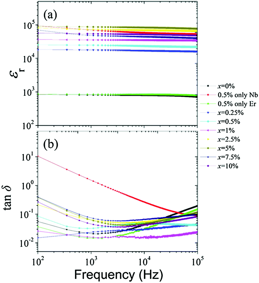 | ||
| Fig. 6 Dielectric permittivity (a) and dielectric loss (b) of all (Er0.5Nb0.5)xTi1−xO2 ceramics in the frequency range of 102 to 105 Hz, measured at room temperature. | ||
Fig. 7(a) and (b) demonstrate temperature dependence of the dielectric properties. 0.25 mol% TiO2 ceramic was selected to conduct the experiment from 80 to 750 K at given frequencies. A stable CP was observed in the ceramics over a wide temperature, from 80 up to 450 K. Polaron dielectric relaxation was observed at around 273 K due to electron hopping motions between Ti4+ and Ti3+.24 The high-temperature dielectric relaxation observed above 450 K is argued to be because of Maxwell–Wagner interfacial polarization.29Fig. 7(c) and (d) show a similar dielectric performance with x = 0.5% and 1%. Dielectric loss of the ceramics shows temperature dependence as illustrated in Fig. 7(b) and (d). These results taken together imply that εr of the doped ceramics in this work were relatively stable over a wide temperature range, which are similar to that reported by Liu's group.10,11 It is noteworthy that tanδ corresponding to Fig. 7(b) and (d) changes significantly with temperature. Based on the previous study,28,30 the other possible mechanisms for CP cannot be excluded by this work.
 | ||
| Fig. 7 Temperature dependence of the dielectric properties. Dielectric permittivity (a) and dielectric loss (b) of ceramics with x = 0.25%, measured from 80 to 750 K at given frequencies. A narrow data break occurs near the room temperature region (approximately 296–298 K), as two experimental set-ups were used for the low-temperature and high-temperature measurements, respectively. Dielectric permittivity (c) and dielectric loss (d) of various doping levels of ceramics, measured from 80 to 423 K and at 1 kHz. | ||
To explore the physical mechanism behind the observations from the material system, the XPS spectra of (Nb + Er) co-doped TiO2 ceramics with various doping levels are presented in Fig. 8(a)–(i). The peaks at the binding energies of 167.7 eV and 168.3 eV for Er 4d5/2 imply an oxidation state of +3 for Er. There is a slight shift in binding energy due to the presence of Er2O3 (secondary phases) which is evident in the XRD results. The XPS results indicate that binding energies of Nb 3d electrons are 207.7 eV and 210.4 eV for 3d5/2 and 3d3/2, respectively, without the presence of other 3d5/2 low binding energies. Their spin–orbit splitting of 2.7 eV is consistent with that of Nb5+ doped TiO2 materials.10 It suggests that there is only one Nb 3d environment present in the ceramic, so that the oxidation state of this Nb is + 5.11 Meanwhile, the position of Ti 2p with 2p3/2 and 2p1/2 corresponding to the binding energies of 458.4 eV and 464.1 eV, respectively, is also clearly shown.31 Compared with the doping level of x = 0.25% and 7.5%, it is noticeable that Ti3+ signals increase with content x. The introduction of Nb5+ is the probable reason for the partial reduction of Ti4+ to Ti3+ in the ceramic as follows:
 | (1) |
| Ti4+ + e → Ti3+ | (2) |
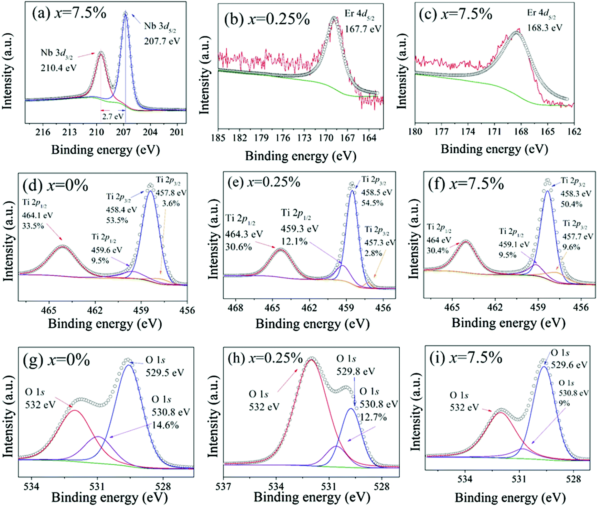 | ||
| Fig. 8 Valence states of the elements in the ceramic with x = 0.25%: Er 4d (b), Ti 2p (e), O 1s (h). Valence states of the elements in the ceramic with x = 7.5%: Nb 3d (a), Er 4d (c), Ti 2p (f), O 1s (i). Valence states of the elements in the pure TiO2 ceramic: Ti 2p (d), O 1s (g). The solid lines are consistent with the peaks, in which the green line stands for background, for the Er element, red lines are the raw data. | ||
Fig. 8(g) shows the O 1s profile of a pure TiO2 ceramics. It was found that O 1s consists of three components, including 529.5 eV for bulk Ti–O, 530.8 eV associated with oxygen vacancies and surface hydroxyl (OH), and 532 eV for adsorbed surface H2O. Previously, it was reported that an increase in the doping level would result in a higher concentration of oxygen vacancies. However, in this experiment, the concentration of oxygen vacancies decreased from 14.6% to 9% as x increased. In principle, doping Er3+ as acceptors requires oxygen vacancies to meet charge compensation conditions, as given in the following equation:
 | (3) |
 | (4) |
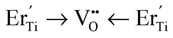
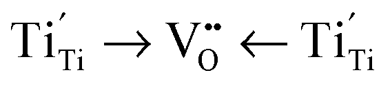
To further explore the mechanism of the observed CP performance, a series of compositional, structural and dielectric analyses of the (EryNb1−y)0.0375Ti0.9625O2 ceramics were conducted. XRD patterns (Fig. S1, ESI†) and SEM images (Fig. S2, ESI†) demonstrate that the ceramics are of pure rutile phases. Element mapping shows that the dopant Er3+ ions are homogeneously distributed in the TiO2 matrix (Fig. S3, ESI†). Based on the impedance Cole–Cole plot (Fig. S4, ESI†) and the results of the dielectric properties (Fig. S5 and S6, ESI†), both intrinsic (electron-pinned defect-dipole) and extrinsic mechanisms are responsible for the observed high-performance CP. In this work, it is expected that there exist both the intrinsic defect-dipole complex/cluster in TiO2:  ,
,  ,
,  ,
,  ,
,  and extrinsic defects:
  . The formation of defect pairs depends on the ionic radius of the dopant. Er3+ has a larger different ionic radius compared to In3+ and Ti4+, this is therefore indicated that the formation of electron-pinned defect dipole clusters as a mechanism to develop high-performance CP materials needs to take into account the relation between the ionic radii of the acceptor, donor, and host ions.
Our (Nb + Er)-modified TiO2 ceramics meet the requirements of Class II ceramic capacitors. Their material requirements are: 1 × 10³ < εr and 0.03 < tanδ < 0.10.34 In combination with the results of CP and low loss, the (Nb + Er)-modified TiO2 ceramics would be promising solid state capacitors and energy storage devices. Further studies are expected for real applications.
4. Conclusion
High-performance CP materials were achieved in the rutile TiO2 ceramics doped with Er3+ and Nb5+. It was found that a doping level of 5 mol% exhibited the optimum overall dielectric properties. Large εr (∼8.6 × 10⁴), sufficiently low tanδ (4%), as well as relatively stable frequency and temperature behaviors of the materials are obtained. According to the analysis of the microstructure, SEM and elemental mapping, Er3+ aggregating at grain boundaries may form extrinsic defects. Both intrinsic and extrinsic defect states could be expected to be responsible for the observed high-performance CP. With the excellent dielectric properties, our results suggest that (Nb + Er)-modified TiO2 ceramics have some advantages compared with the conventional capacitor materials. The developed materials are favorable for fully solid-state capacitor and high-energy-density storage applications.
Acknowledgements
This work was supported by the grant from Research Grants Council of Hong Kong (GRF No. PolyU 153004/14P).References
- C. C. Homes, T. Vogt, S. M. Shapiro, S. Wakimoto and A. P. Ramirez, Science, 2001, 293, 673 CrossRef CAS PubMed.
- S. Krohns, P. Lunkenheimer, S. Meissner, A. Reller, B. Gleich, A. Rathgeber, T. Gaugler, H. U. Buhl, D. C. Sinclair and A. Loidl, Nat. Mater., 2011, 10, 899 CrossRef CAS PubMed.
- C. C. Homes and T. Vogt, Nat. Mater., 2013, 12, 782 CrossRef CAS PubMed.
- H. Han, C. Voisin, S. Guillemet-Fritsch, P. Dufour, C. Tenailleau, C. Turner and J. C. Nino, J. Appl. Phys., 2013, 113, 024102 CrossRef.
- Z. Gai, Z. Cheng, X. Wang, L. Zhao, N. Yin, R. Abah, M. Zhao, F. Hong, Z. Yua and S. Dou, J. Mater. Chem. C, 2014, 2, 6790 RSC.
- P. Lunkenheimer, S. Krohns, S. Riegg, S. G. Ebbinghaus, A. Reller and A. Loidl, Eur. Phys. J.: Spec. Top., 2010, 180, 61 CrossRef.
- S. Guillemet-Fritsch, Z. Valdez-Nava, C. Tenailleau, T. Lebey, B. Durand and J. Y. Chane-Ching, Adv. Mater., 2008, 20, 551 CrossRef CAS.
- M. T. Buscaglia, M. Viviani, V. Buscaglia, L. Mitoseriu, A. Testino, P. Nanni, Z. Zhao, M. Nygren, C. Harnagea, D. Piazza and C. Galassi, Phys. Rev. B: Condens. Matter Mater. Phys., 2006, 73, 064114 CrossRef.
- M. A. Subramanian, D. Li, N. Duan, B. A. Reisner and A. W. Sleight, J. Solid State Chem., 2000, 151, 323 CrossRef CAS.
- W. Hu, Y. Liu, R. L. Withers, T. J. Frankcombe, L. Norén, A. Snashall, M. Kitchin, P. Smith, B. Gong, H. Chen, J. Schiemer, F. Brink and J. Wong-Leung, Nat. Mater., 2013, 12, 821 CrossRef CAS PubMed.
- W. B. Hu, K. Lau, Y. Liu, R. L. Withers, H. Chen, L. Fu, B. Gong and W. Hutchison, Chem. Mater., 2015, 27, 4934 CrossRef CAS.
- X. Cheng, Z. Li and J. Wu, J. Mater. Chem. A, 2015, 3, 5805 CAS.
- X. Wei, W. Jie, Z. Yang, F. Zheng, H. Zeng, Y. Liu and J. Hao, J. Mater. Chem. C, 2015, 3, 11005 RSC.
- X. Lü, W. Yang, Z. Quan, T. Lin, L. Bai, L. Wang, F. Huang and Y. Zhao, J. Am. Chem. Soc., 2014, 136, 419 CrossRef PubMed.
- J. Yu, J. Low, W. Xiao, P. Zhou and M. Jaroniec, J. Am. Chem. Soc., 2014, 136, 8839 CrossRef CAS PubMed.
- X. Lü, F. Huang, X. Mou, Y. Wang and F. Xu, Adv. Mater., 2010, 22, 3719 CrossRef PubMed.
- C. T. Dervos, E. F. Thirios, J. Novacovich, P. Vassiliou and P. Skafidas, Mater. Lett., 2004, 58, 1502 CrossRef CAS.
- S. Chao and F. Dogan, J. Am. Ceram. Soc., 2011, 94, 43 CrossRef.
- R. T. Shannon, Acta Crystallogr., Sect. A: Cryst. Phys., Diffr., Theor. Gen. Crystallogr., 1976, 32, 751 CrossRef.
- Y. Zhang, C. X. Harris, P. Wallenmeyer, J. Murowchick and X. Chen, J. Phys. Chem. C, 2013, 117, 24015 CAS.
- J. B. Wu, C. W. Nan, Y. H. Lin and Y. Deng, Phys. Rev. Lett., 2002, 89, 217601 CrossRef PubMed.
- U. Wahl, A. Vantomme, J. De Wachter, R. Moons, G. Langouche, J. G. Marques and J. G. Correia, Phys. Rev. Lett., 1997, 79, 2069 CrossRef CAS.
- M. Needels, M. Schluter and M. Lannoo, Phys. Rev. B: Condens. Matter Mater. Phys., 1993, 47, 15533 CrossRef CAS.
- L. X. Pang, H. Wang, D. Zhou and X. Yao, J. Mater. Sci., 2010, 21, 1285 CAS.
- W. Y. Wang, D. F. Zhang, T. Xu, X. F. Li, T. Zhou and X. L. Chen, J. Alloys Compd., 2002, 335, 210 CrossRef CAS.
- R. Bouchet, A. Weibel, P. Knauth, G. Mountjoy and A. V. Chadwick, Chem. Mater., 2003, 15, 4996 CrossRef CAS.
- Q. Wang, O. Varghese, C. A. Grimes and E. C. Dickey, Solid State Ionics, 2007, 178, 187 CrossRef CAS.
- J. Li, F. Li, Y. Zhuang, L. Jin, L. Wang, X. Wei, Z. Xu and S. Zhang, J. Appl. Phys., 2014, 116, 074105 CrossRef.
- C. Wang, N. Zhang, Q. Li, Y. Yu, J. Zhang, Y. Li and H. Wang, J. Am. Ceram. Soc., 2015, 153, 148 CrossRef.
- W. Dong, W. Hu, A. Berlie, K. Lau, H. Chen, R. L. Withers and Y. Liu, ACS Appl. Mater. Interfaces, 2015, 7, 25321 CAS.
- G. S. Li, J. Boerio-Goates, B. F. Woodfield and L. P. Li, Appl. Phys. Lett., 2004, 85, 2059 CrossRef CAS.
- M. F. Yan, R. M. Cannon and H. K. Bowen, J. Appl. Phys., 1983, 54, 764 CrossRef CAS.
- U. Wahl, A. Vantomme, J. De Wachter, R. Moons and G. Langouche, Phys. Rev. Lett., 1997, 79, 2069 CrossRef CAS.
- R. K. Pandey, W. A. Stapleton, J. Tate, A. K. Bandyopadhyay, I. Sutanto, S. Sprissler and S. Lin, AIP Adv., 2013, 3, 062126 CrossRef.
Footnote |
| † Electronic supplementary information (ESI) available. See DOI: 10.1039/c6cp02236g |
| This journal is © the Owner Societies 2016 |