
 Open Access Article
 This Open Access Article is licensed under a Creative Commons Attribution-Non Commercial 3.0 Unported Licence
Unraveling energy conversion modeling in the intrinsic persistent upconverted luminescence of solids: a study of native point defects in antiferromagnetic Er2O3
Bolong
Huang
Department of Applied Biology and Chemical Technology, The Hong Kong Polytechnic University, Hung Hom, Kowloon, Hong Kong SAR, China. E-mail: bhuang@polyu.edu.hk
First published on 19th April 2016
Abstract
We investigated the mechanism of the intrinsic persistent luminescence of Er2O3 in the A-type lattice based on first-principles calculations. We found that the native point defects were engaged in mutual subtle interactions in the form of chemical reactions between different charge states. The release of energy related to lattice distortion facilitates the conversion of energy for electrons to be transported between the valence band and the trap levels or even between the deep trap levels so as to generate persistent luminescence. The defect transitions that take place along the zero-phonon line release energy to enable optical transitions, with the exact amount of negative effective correlation energy determined by the lattice distortions. Our calculations on the thermodynamic transition levels confirm that both the visible and NIR experimentally observed intrinsic persistent luminescence (phosphor or afterglow) are related to the thermodynamic transition levels of oxygen-related defects, and the thermodynamic transition levels within different charge states for these defects are independent of the chemical potentials of the given species. Lattice distortion defects such as anion Frenkel (a-Fr) pair defects play an important role in transporting O-related defects between different lattice sites. To obtain red persistent luminescence that matches the biological therapeutic window, it is suggested to increase the electron transition levels between high-coordinated O vacancies and related metastable a-Fr defects; a close-packed core–shell structure is required to quench low-coordinated O-related defects so as to reduce the green band luminescence. We further established a conversed chain reaction (CCR) model to interpret the energy conversion process of persistent luminescence in terms of the inter-reactions of native point defects between different charge states. It is advantageous to use the study of defect levels combined with formation energies to suggest limits to doping energy and explain photostimulated luminescence in terms of native point defects.
Introduction
Persistent luminescence refers to an optical phenomenon1–3 in which a material is excited by high-energy radiation such as UV light and the resulting visible luminescence emission remains visible for an appreciable time, from minutes to hours after the stoppage of the excitation.4 It exhibits greener and more efficient features than conventional luminescence processes.5,6 It shows the most promise for applications in bioimaging because no external excitation is needed on tissue.7,8 Current demands from biological and medical scientists are for red emissions (therapeutic window in biomedicine: 600–700 nm) and even emissions in the NIR region (highly tissue-penetrating light: 700–1000 nm), which are optimal for the diagnosis and treatment of living tumor cells via in vivo imaging technology.8–13Recent progress implies that lanthanide oxide materials are novel upconversion luminescence materials that hold great potential for persistent upconverted luminescence.14 It is uncommon that lanthanide sesquioxides themselves display persistent luminescence, especially based on the upconversion character of electron transport. Tanner et al. concluded that this property is not due to unique electronic characteristics, as in the case of the 4f–5d or 4f–4f transitions in Er2O3, because the experimentally reported persistent luminescence emission bands appear to be the same for different Ln2O3 (Ln = Pr, Nd, Sm and Er).14,15 Accordingly, this persistent luminescence is attributed to subtle interactions between different states of native point defects, based on the experience of our previous investigations.16–18 Unfortunately, the relationship between electron transport assisted by the levels of native defects and the properties of persistent upconverted luminescence is still far from being fully understood, especially at the electronic level. This knowledge gap not only impedes the process of designing new generations of persistent luminescence devices but also prevents the further development of existing technology. Further investigations to fill this gap are of great significance for the relevant science and related technological applications.
In persistent luminescence, the driving force for extensive theoretical investigations is related to the current consensus as summarized by experiments, in which two dominant factors determine the performance of persistent luminescent materials: activators and traps. The emission wavelength is mainly determined by the intraconfigurational levels provided by activators. The intensity and duration of persistent luminescence are governed by trap centers in terms of native point defects in the lattice or co-dopants. The exact balance of activators and traps within the electronic structure decides the selection of their optimal combinations.
However, some recent experiments have refreshed our understanding of the role of trap levels in persistent luminescence and given rise to our new interest in the native point defects of luminescent solids. In an experiment that controlled trap levels carried out by Maldiney et al.,19 measurements of thermal glow (or thermally stimulated luminescence, TSL) were benchmarked with respect to the trap levels provided by various rare earth (RE) ion dopants. The deepest trap levels, which were induced by Dy3+, did not give rise to the longest duration of luminescence. In contrast, Pr3+, for which the levels were the second closest to the conduction band edge, provided the longest duration and maintained the highest intensity, where the trap levels were even higher than the levels of native O vacancies. Therefore, TSL measurements under conditions of varying temperature cannot give a perfect quantitative description of the levels of native point defects and related variations in behavior for persistent phosphors. This arises because native point defects in specific charge states may be modified by the external thermal conditions during TSL. This consideration provides the idea that types of native defect such as Schottky (in the rock salt simple cubic lattice) or Frenkel (in the fluorite lattice) pair defects play a significant role that is independent of the chemical potentials in a thermal or optical disequilibrium state with charge neutrality maintained.
The interaction of the levels of different point defects is a significant issue. As known from previous work,16 we found that the native point defects in the host materials not only produce local lattice distortion or charge density anomalies, but also induce unique localized electron levels in the fundamental optical band gap that are either occupied or empty. Therefore, the stabilities and concentrations of the native point defects in the host materials are quite important in studies of persistent phosphors. Recent work performed by De Vos et al. has provided supportive information via calculations using local density formalism.20 They found that antisite defects have greater stability and their distance (with respect to the density) is closely correlated to the overall stability of the material based on Zn–Ga oxide alloys (ZnGa2O4), which have also been investigated by Karazhanov et al.21 using DFT calculations. Their localized gap states exhibit a qualitative trend to support their model.
The actual situations regarding the properties of the materials are complicated and it is also necessary to consider the participation of all possible defects and their contributions to the transition levels. This context can lead us to explain an experiment that shows that the electron transport or photocurrent in a zinc gallate nanowire is very sensitive to the pressure of oxygen and the temperature, which implies the importance of oxygen-related defects such as oxygen vacancies and interstitials.22,23 However, relative errors in calculations may exceed 30%, whereas trends in physical chemistry show the significance of discussing the defect states in the spinel lattice in such defective Zn–Ga oxide alloys in order to understand persistent phosphors from different aspects.20 A different systematic study by Zeng et al.24 shows that both anion- and cation-related defects play important roles in accommodating charge carriers for transport and energy conversion to generate persistent luminescence. Therefore, it is necessary to have a preliminary discussion of different native point defects in a simplified model of the A-type lattice of Er2O3, to investigate their energy conversion mechanisms, and to provide a useful reference for further experiments14 and various applications.
Here, we discuss the models of luminescence that relate to F-centers and the energy conversion process, which reflect different optical transitions. As is well known, the optical behavior of typical defects in solids is mostly governed by strong electron–phonon coupling, which leads to a broadened photon–electron transition following an evident Stokes shift between the absorption and emission spectra.25 Accordingly, another important issue to be solved is the defect reaction model for persistent luminescence, to identify the location of the nearly continuous energy source that generates a persistent optical transition. Actually, if defect-related transitions follow the zero-phonon line (ZPL) between different optical transition states, optical absorption and emission will be accomplished with high efficiency in both optical quantum yield and energy conversion.26,27 Our question is what happens if the two optical transition states are replaced by two complementary charged defects, which react via charge transfer and electron transitions in closed cycles along the ZPL. This implies that the lattice distortions during these reactions will support electron transfer between different optical transition levels, ideally with an exact amount of negative effective correlation energy (−Ueff), which is shown in Fig. 1.
 | ||
| Fig. 1 Schematic diagram illustrating the model of persistent luminescence based on energy conversion induced by native point defects. | ||
Here, we also discuss such native complementary charged point defects, which are not only formed for energy conversion but also act as donor–acceptor pairs (DAP), with a DAP band within the forbidden band gap of the host material, as a paired activator for electron–hole recombination and the release of photons. In addition, these DAP bands actually fix the center of the luminescence band at a specific energy level by means of restricted optical transitions via a closed cycle along the ZPL related to −Ueff. A similar concept has been successfully utilized in other solid functional materials using our theoretical modeling.28–30
With the aim of elucidating the relevant scientific issues via our theoretical methodology, this paper will focus on erbium sesquioxides to study their electronic structures, optical properties, and thermodynamic and optical transition levels. A systematic investigation will start from the inherent principles that govern the interactions among the microscopic structures, levels of native defects, localized states and mechanisms of persistent luminescence.
Calculation setup
As is well known, three stable lattice structures have been observed for lanthanide sesquioxides (Ln2O3), namely, hexagonal (A-type, P![[3 with combining macron]](https://www.rsc.org/images/entities/char_0033_0304.gif) m1), monoclinic (B-type, C12/m1), and bixbyite (C-type, Ia).31 We chose the antiferromagnetic (AFM) ordered lattice for modeling the structure of Er2O3, as this lattice has a ground state below 4 K (the Néel temperature). This was also done in the effort to save unnecessary computational cost in investigating a trend in the physical chemistry of defect states, as well as in the modeling of energy conversion in such oxides, without making an absolutely conclusive determination.
m1), monoclinic (B-type, C12/m1), and bixbyite (C-type, Ia).31 We chose the antiferromagnetic (AFM) ordered lattice for modeling the structure of Er2O3, as this lattice has a ground state below 4 K (the Néel temperature). This was also done in the effort to save unnecessary computational cost in investigating a trend in the physical chemistry of defect states, as well as in the modeling of energy conversion in such oxides, without making an absolutely conclusive determination.
On the other hand, if we consider nanoparticles in the real world the coordination of oxygen could be very different. Experimentally reported persistent luminescence is based on powder samples of Er2O3. Therefore, we used the simplest lattice structure with various O coordination numbers and antiferromagnetic behaviors. We thus modeled erbium sesquioxides (Er2O3) using the hexagonal (A-type) lattice with the Pm1 space group.
Accordingly, in this study of defects, to reduce the influence of variations in the lattice on the f-level of Er3+ ions, we constrained our structural model of the host materials to an A-type lattice similar to those of La2O3 or Ce2O3, with similar treatment as in the work done by Gillen et al.32 and Jiang et al.33,34 Note that a similar simplification of the structural model has been utilized in work by one of our previous collaborators17,35 in order to investigate the levels of native oxygen-related defects in La2O3 (A-type), Lu2O3 (C-type) and LaLuO3 (distorted C-type) uniformly within a model of an A-type lattice,35 as well as other similar high-K oxides.36,37
The lattice relaxation of Er2O3 in the ground state was performed at the PBE or PBE+U level by the CASTEP code,38 because PBE, as the first ‘Jacob’s ladder’ in DFT, has been proven to be reliable enough for the structural relaxation and internal geometrical optimization of solids based on 4f- or 5f-levels,39 regardless of whether ultrasoft or norm-conserving pseudopotentials are used. Theoretical studies show that pseudopotentials in solids based on f-level have a minor or negligible influence on the lattice parameters in DFT or DFT+U.17,18,40–43 However, Hubbard U parameters induce an extra error in lattices when we need them for improving the accuracy of electronic structures, if we select them carelessly or they are calculated without self-consistent determination.17,18,40–43
We decided to select five orbital components, namely, 4f, 5s, 5p, 5d, and 6s to represent the valence states of the Er atom. We chose norm-conserving pseudopotentials because in the valence electrons region they can reflect the all-electron behavior with an overlapping integral factor of |S-matrix| = 1, which is evidently different from ultrasoft pseudopotentials.44,45 The overlapping integral factor will reduce the contribution of the Hubbard potential corrections when applied to the charge density of the single-electron semi-orbitals. Using the OPIUM code for generation with the recent RRKJ optimization method,46 we “tailor-made” the norm-conserving pseudopotentials within the framework of the most popular KB (Kleinman–Bylander) projectors47 and non-linear partial-core corrections,48 which have won recognition as a result of our theoretical developments.17 We specifically chose the scalar-relativistic averaging scheme49 with the aim of dealing with the complicated local hybridization of semi-core 4f–5d orbitals and the relativistic effect of heavy Er3+ ions, which also describes the spin–orbit coupling effect well at a numerical level.
With the plane-wave basis set, it is highly recommended to carefully extend the cutoff energy to 750 eV to describe the five different orbital components of the valence electrons of Er3+, as well as the strongly localized states induced by the 2p orbitals of O. To guarantee convergence and avoid charge/spin out-of-sync ‘sloshing’, we uniformly chose the ensemble DFT (EDFT) method of Marzari et al.50 For the k-point sampling mesh, we chose a grid of 7 × 7 × 4 for all related reciprocal space integration for the primitive cell of Er2O3. By the above settings, the convergence tolerance of the calculations of total energy was set to no higher than 5.0 × 10⁻⁷ eV per atom, and the optimization by Hellmann–Feynman forces in calculations of defects was accomplished to a level lower than 0.01 eV Å−1. For calculations of supercell-based defects, a 60-atom 2 × 2 × 3 supercell was used for Er2O3. The Baldereschi special k-point (1/4, 1/4, 0)51 with the gamma center off was self-consistently selected. Regarding the geometry relaxation, an algorithm based on the Broyden–Fletcher–Goldfarb–Shanno (BFGS) method was used throughout all calculations of bulk and defect supercells.
As we realized from theoretical studies, the electronic states that occur in the fundamental optical gap are less sensitive to the nonlinearity of Hubbard U parameters. Therefore, we chose the rotational-invariant type DFT+U method developed by Anisimov.52 To reduce the influence of the localized hole states produced by the 2p orbitals of O sites, self-consistently determined Hubbard U potentials were also applied to the O 2p orbitals, which have reached a consensus41,53–55 in many oxide materials. Thus, it is necessary to consider self-energy corrections to both f- and p-orbitals for rare earth oxides.17,18,42
For all calculations of native point defect states in Er2O3, we used self-consistent determination for the U correction to the localized 4f orbitals to correct the on-site Coulomb energy of the spurious self-energy of electrons. In previous work, we have established a method for determining the on-site self-energy of electrons and the related relaxation of the wavefunction in orbitals so as to obtain accurate orbital eigenvalues for electronic structures.42 For details of the process, refer to the previous work. With our self-consistent determination process, the on-site Hubbard U parameters for the 4f orbitals of Er and the 2p orbitals of 6-fold coordinated O and 4-fold coordinated O were found to be 9.72 eV, 5.73 eV and 5.49 eV, respectively. For the pseudopotentials of Er used for calculation, we similarly chose a nonlinear core correction technique for correcting the overlap of valence-core charge density in such heavy-fermion elements; a detailed discussion of such a method has been presented in a previous study of the native point defects in CeO2.17,18 The valence electron configuration for the pseudopotentials we chose for the generation was 4f11, as the ground-state configuration for Er3+. All the DFT+U calculations were performed in a theoretical scheme using the norm-conserving pseudopotentials. This helped us to reflect the all-electron behavior of the valence electrons, especially regarding the subtle effects of the 4f electrons and outer 6s electrons.
For the equation that was used for calculations of the formation energy of defects in different charge states (q), an overall supercell was established and remained constantly based on the ground-state relaxed primitive cell, to reduce the side effects of changes in enthalpy due to variations in the cell. The formation energy of a target defect Hq in a specific charge state q can be described via a relation between the positions of the Fermi energy (EF) and the chemical potential Δμ of the species of defect α, which is shown as follows:
 | (1) |
Results and discussion
Bulk A-type Er2O3
The A-type lattice of Er2O3 with the Pm1 space group has been predicted based on a method used in our previous work.42 In this symmetry, the high-symmetry points Γ, K, and M are relatively significant in the first Brillouin zone (BZ). The ground-state relaxed structure has lattice parameters of a = 3.632 Å and c = 5.763 Å, respectively. From Fig. 2, calculations of the band structure show that the band gap of Er2O3 in the A-type lattice is 5.506 eV using GGA+U calculations with the U parameters for O 2p and Er 4f predicted from the previous work.42 The indirect band gap of 5.506 eV is from Γ to K, whereas the direct optical transition gap of Γ → Γ is about 5.8 eV, which is close to the average band gap of high-K dielectric oxide materials. Gillen et al.32 and Jiang et al.33,34 have performed calculations on lanthanide sesquioxides using different methods, respectively. The HSE functional used by Gillen et al. shows the band gap to be 5.30 eV and Jiang et al. reported a band gap of 5.22 eV by the GW method. These are both 0.2 eV lower than the experimentally reported value of 5.49 eV,57 whereas ours is close to the experimentally reported 5.5 eV.57 There is a small increase of 0.2 eV from the experimental result from Prokofiev et al.58 The width of the valence band (VB) is about 4–5 eV, which consists of the levels of O 2p orbitals. The three occupied 4f levels are located about 2.8 eV, 4.5 eV and 5.8 eV, respectively, below the valence band maximum (VBM, 0 eV in Fig. 2), with an overlap from O 2p levels in the VB. The unoccupied 4f level is around 9 eV above the VBM and remains in the conduction band (CB). The conduction band minimum (CBM) mainly consists of Er 5d orbitals.
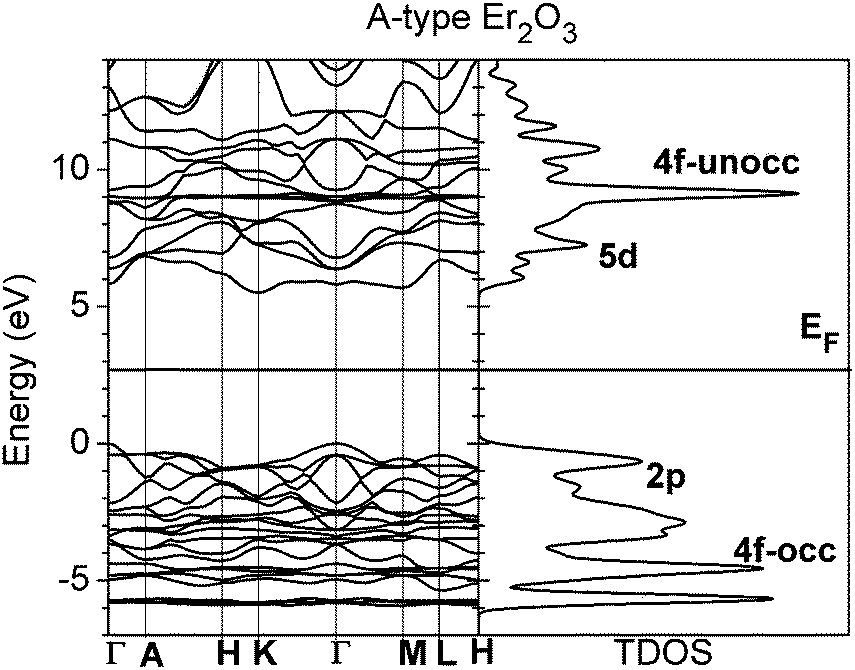 | ||
| Fig. 2 Band structure and TDOS of bulk Er2O3 in A-type lattice. | ||
Regarding the bulk formation enthalpy of crystalline Er2O3, 2μEr + 3μO = ΔHf(Er2O3), the experimentally observed formation enthalpy of Er2O3 is reported to lie within the range from −19.67 to −19.73 eV at T = 298 K (−1897.859 or −1904.2 kJ mol−1![[thin space (1/6-em)]](https://www.rsc.org/images/entities/char_2009.gif) 60). Our calculations give −19.17 eV by the GGA+U method (Uf = 9.72 eV for 4f of Er, Up = 5.49 eV for 2p of O4, and Up = 5.73 eV for O6) at T = 0 K (ground state), which agrees well with the experimental value at T = 298 K (with a relative error of only 2.5%), as well as a correct physical trend (with a value about 0.5 eV higher), as the monoclinic phase of Er2O3 at low temperatures (around 300 K) is more stable than the hexagonal phase (A-type lattice) of Er2O3. Our method shows greater advantages than the method of plain GGA calculations.61
60). Our calculations give −19.17 eV by the GGA+U method (Uf = 9.72 eV for 4f of Er, Up = 5.49 eV for 2p of O4, and Up = 5.73 eV for O6) at T = 0 K (ground state), which agrees well with the experimental value at T = 298 K (with a relative error of only 2.5%), as well as a correct physical trend (with a value about 0.5 eV higher), as the monoclinic phase of Er2O3 at low temperatures (around 300 K) is more stable than the hexagonal phase (A-type lattice) of Er2O3. Our method shows greater advantages than the method of plain GGA calculations.61
Oxygen vacancy (VO)
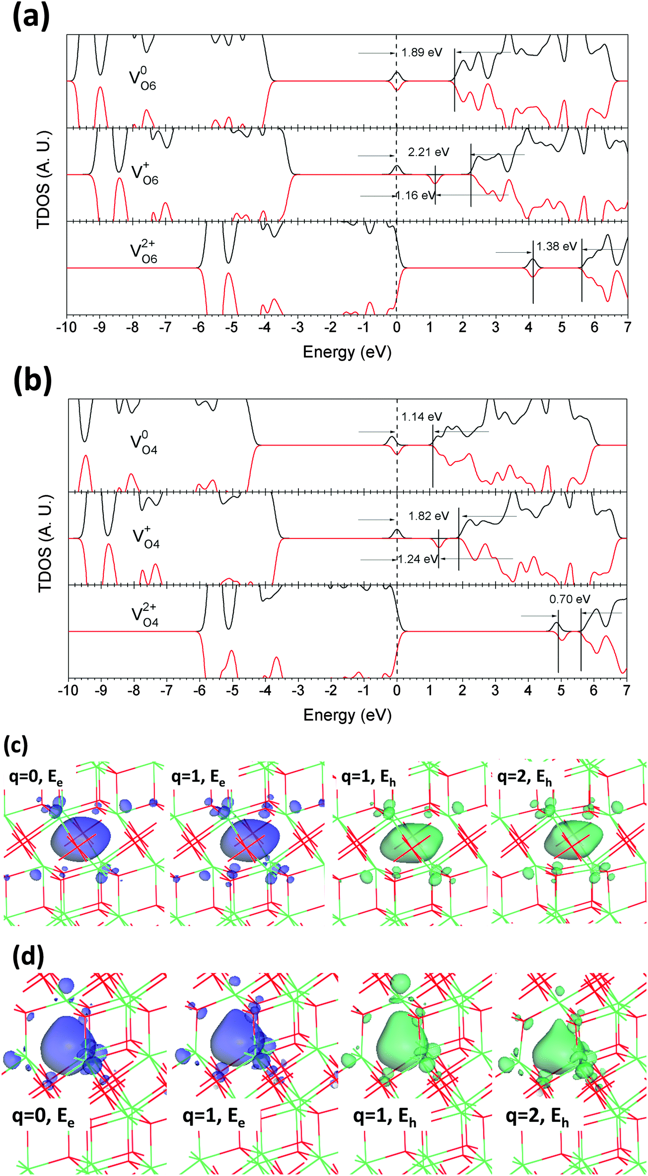
The VO is the most common native point defect in oxides, and is usually the initial equilibrium stable state for most oxide materials. Its influence on their electrical and optical properties is rather significant. As many studies of oxides by Lucovsky et al.62 show, the VO usually induces effects on the O K pre-edge of XAS spectra in optical fundamental absorption experiments, which have been observed in most common oxides such as trigonal HfO2, monoclinic ZrO2, rutile TiO2, bixbyite Lu2O3, SrTiO3, LaTiO3, Gd(Sc, Ti)O3, etc.We studied the VO in Er2O3 in charge states of 0, +1, and +2. Considering the coordination of O ions, there are two different O sites in Er2O3: 6-fold coordinated and 4-fold coordinated (O6 and O4, respectively). Their vacancy sites are shown as VO6 and VO4, respectively. The neutral V0O6 and V0O4 both leave two localized electrons at nearby Er sites with antiferromagnetic (AFM) spin behaviors. Fig. 3(a) shows the total density of states (TDOS) of V0O6. The two localized states are 1.89 eV below the CBM with spin-up and -down together, whereas the value is 1.14 eV for V0O4, as shown in Fig. 3(b). In combination with our analysis of the projected DOS (PDOS), the nearby empty Er 5d orbitals accommodate these localized electrons (∼1.25 e for V0O6) and there is also some extent of hybridization with the first nearest-neighboring 4-fold coordinated O 2p orbitals (∼0.90 e for V0O6). Thus, it is also shown that the O6 and O4 sites have very different energy levels within the crystal lattice that could localize electrons. These two localized electrons are angular-momentum degenerate, giving distorted s-like wavefunctions. A similar case has been found in our previous work.16
 | ||
| Fig. 3 (a) TDOS of VO6 in neutral (V0O6), singly positive (V+O6), and doubly positive (V2+O6) charge states. The dashed line denotes the highest occupied level for electrons. (b) TDOS of VO4 in neutral (V0O4), singly positive (V+O4), and doubly positive (V2+O4) charge states. Localized electron and hole orbitals at the relaxed VO6 (c) and VO4 (d) sites (Er = green, O = red). Formation energies of VO6 (e) and VO4 (f) below the O- and Er-rich chemical potential limits. | ||
Both V+O6 and V+O4 provide only one excess electron at the O vacancy site but give rise to two localized states within the band gap with one empty state. This arises because the single excess electron occupies the orbital that hybridizes with O 2p and Er 5d exhibits splitting into bonding and anti-bonding states, as shown in Fig. 3(a) and (b), with different energy intervals due to the different on-site Coulomb interactions of O6 and O4 sites. The localized orbitals of these states are shown in Fig. 3(c) and (d). The filled trap level of V+O6 lies 2.21 eV below the CBM and 1.16 eV lower than its empty state, whereas for V+O4 these values are 1.82 eV and 1.24 eV, respectively. Compared with previous work on CeO2 and CaS,16,17 we find that for covalent charge-transfer metal oxides (CeO2,17 TiO2, etc.) the V+O displays paramagnetic behavior, whereas for ionic metal oxides or sulfides such as Er2O3, ZnO, CaS,16etc., it exhibits ferromagnetic (FM) behavior owing to the absence of energy degeneracy in the hybridized orbital in the vicinity of anion vacancy sites. From another perspective, the empty state is actually a localized hole trap level in Er2O3 with VO. Electron energy loss spectroscopy (EELS) experiments give evidence that the empty d orbital of the cation tends to hybridize with the s or p orbital of an anion to form an ionic hole trap.63
The V2+O6 and V2+O4 revert to the AFM state with two spin-aligned empty states in the gap. This shows that the empty hybridized orbital (2p–5d) has levels with different spins. These are 1.38 eV and 0.70 eV below the CBM for V2+O6 and V2+O4, respectively. From Fig. 3(a) and (b), we see that the VB edges are almost unchanged within all charge states for both V2+O6 and V2+O4, whereas the CB edges exhibit evident variations near the CBM, which indicates that the localized electrons left by the O vacancy interact strongly with localized Er 5d orbitals of the host lattice, while having less effect on delocalized 2p orbitals of the host lattice. This implies that the localized electrons left by the O vacancy are predominantly from neighboring Er sites. Fig. 3(c) and (d) show that V0O6 and V0O4 have a minor lattice distortion effect, whereas V+O6 and V+O4 push the six Er sites outward while attracting the nearest O sites inward, and this occurs to a greater extent for V2+O6 and V2+O4. The orbitals with localized electrons in these charge states of the O vacancy have s-like wavefunctions, whereas the localized hole states display some extent of hybridized Er 5d orbitals.
Considering the formation energies, Fig. 3(e) and (f) show that both VO6 and VO4 in Er2O3 are defects with positive effective correlation energies (+Ueff) of 0.99 eV and 0.53 eV, respectively. The role of this effect in persistent luminescence has been discussed in the work of Zeng et al.24 and our previous work.16 This shows that the process of 2V+O → V0O + V2+O is an endothermic chemical reaction. We see from Fig. 3(c) and (d) that each charge state of VO is followed to a different extent by local structural distortions, but the costs of these thermally ionized VO defect states cannot be compensated by the lattice distortions. Therefore, they exhibit a positive Ueff, and V+O is also proved to be a widely existing defect as found by electron spin resonance (ESR) measurements, which has the potential to be an F+ center. V0O6 and V0O4 have very similar formation energies of 7.40 eV and 7.48 eV below the O-rich chemical potential limit, whereas these are as low as 0.05 eV and 0.13 eV, respectively, in Er-rich conditions; this shows a consistent physical trend of rather stable O vacancy defects in high-K oxides such as HfO2 as found by Ka et al.64 The relatively low formation energy indicates that the O vacancy is energetically favorable in erbium sesquioxides, as in deficient erbium oxides ErO2. The V+O6 defect has energies of 3.31 eV and −4.04 eV below the O-rich and Er-rich limits, respectively. The thermodynamic transition levels of the (0/+) and (+/2+) states are 4.09 eV and 3.10 eV above the VBM respectively. V+O4 is shown to be more stable than V+O6, as their formation energies are 3.10 eV and −4.25 eV with transition levels of 4.38 eV and 3.85 eV for the (0/+) and (+/2+) states, respectively.
As carefully learned from the results of Pan et al.,65 we see that a discussion of the oxygen vacancy is meaningful, as an experiment on Er2O3 by Pan et al.65 shows that the oxygen vacancy controls the electrical conduction, which is related to the transport of charge carriers. More importantly, an experiment by Hao et al.14 shows that the effect of the absorption of water molecules (H2O) on nanoparticles of Er2O3 will induce the unexpected quenching or lowering of optical excitation transitions, as shown from a comparison of emission spectra between vacuum and ambient conditions (Fig. 2 in ref. 14). Such absorption of moisture is in fact due to the existence of native oxygen vacancy defects in Er2O3, as confirmed by Pan et al.65 This effect has also been found by Tang et al. in another oxide system (Bi4−xEuxTi3O12).66
On the other hand, Pan et al. have reported further on the effects of oxygen vacancies in other lanthanide sesquioxides such as Lu2O3.67 They show that both oxygen vacancies and interstitials (non-lattice defects) are good charge carrier centers so as to enable filament conduction in Lu2O3.67 We similarly deduce that the oxygen-related defects play a similar role in Er2O3. Therefore, it is very useful to provide the results of such preliminary theoretical calculations as a reference for their experiments and applications.
O interstitial (Oi)
The Oi in Er2O3 produces complicated localized electron and hole states that interact with surrounding lattice sites with different local bonding and charge states. As shown in previous work, the Oi in metal oxides such as CeO217 may form peroxides with O–O homopolar bonds, which gives rise to π-electrons localized along the O–O bonds near Oi sites. The neutral Oi in Er2O3 forms an O–O bond and induces four localized π-electron levels below the VBM (from −7 to −8 eV), as shown in Fig. 4(a). Other localized occupied states are about 0.2 eV above the VBM. The anti-bonding π-electron states remain at the CBM as π* orbitals of O–O bonds formed by Oi. | ||
| Fig. 4 (a) TDOS of Oi in neutral (O0i), singly negative (O−i), and doubly negative (O2−i) charge states. The dashed line denotes the highest occupied level for electrons. (b) Localized electron and hole orbitals at the relaxed Oi site (Er = green, O = red). (c) Formation energies of Oi below the O- and Er-rich chemical potential limits. | ||
The O−i in Er2O3 produces clear localized hole states in the band gap 2.51 eV above the VBM, whereas other occupied electron states that are observable remain near the VBM and are 0.2 eV higher. However, these two edge states display a minor ferromagnetic effect as spin-misaligned. The states below the VBM that have shifted into the VB consist of O 2p levels.
The O2−i in Er2O3 produces six localized electron states near the VBM with intervals of about 0.15 eV that are spin-aligned. This arises because the Oi accepts two excess electrons and thus gives rise to a 2p6 valence electron configuration, in which bonding states are localized near the VBM. We see from Fig. 4(a) that these localized states exhibit antiferromagnetic behavior.
Fig. 4(b) shows the localized electron and hole orbitals near the directions of the O–O bonds formed by the relaxed Oi sites. We see that all the orbitals are localized, which shows the evident trapping behavior exhibited by Oi. The π-electron orbital of O0i is localized around the O–O bond and the nearest-neighboring O sites. The O−i produces hybridized pz–dyz orbitals vertically in the cell along the O–O bond.
Fig. 4(c) shows that the Oi in Er2O3 is a defect center with a negative Ueff in the transition state of (2−/0), with a value of Ueff of −0.45 eV. This means that the Oi chemical reaction process, 2O−i → O0i + O2−i, is an exothermic process, and the thermodynamic transition level of (2−/0) is 2.16 eV above the VBM. This means that electron spin resonance (ESR) measurements detect a very low density of O−i defects, because only O0i and O2−i can stably exist in the lattice and both eigenstates can be stabilized in the gap. The energy cost of the formation of these defects can be compensated by the local lattice distortions.
We see from Fig. 4(c) that below the O-rich potential limit the O0i has a formation energy of 2.16 eV in the Er2O3 lattice, whereas the value is 6.48 eV for O2−i below the O-rich limit. The O−i has an energy cost of 4.55 eV below the O-rich limit, whereas according to the effect of −Ueff this state cannot widely exist in the lattice as it has a low possibility, owing to being constrained by the effect of −Ueff. Thus, Oi is unlikely to form deep hole trap centers in Er2O3, at least in the A-type lattice environment. This is consistent with our results deduced from the negative Ueff for the (−2/0) state.
Er vacancy (VEr)
The neutral VEr in Er2O3 (V0Er) gives rise to three localized holes that occupy the nearby O sites. The single-particle levels (TDOS) shown in Fig. 5(a) confirm that there are three localized deep hole trap levels at about 1.86 eV below the CBM. One of these holes is spin-up, whereas the other two holes remain spin-down. The V−Er has two localized hole traps that are 2.88 eV and 2.58 eV below the CBM, respectively, and are spin-misaligned. Fig. 5(b) shows that there are three individual localized empty p–π orbitals around the nearest-neighboring O sites as potential electron-accepting centers. | ||
| Fig. 5 (a) TDOS of VEr in neutral (V0Er), singly negative (V−Er), doubly negative (V2−Er), and triply negative (V3−Er) charge states. The dashed line denotes the highest occupied level for electrons. (b) Localized hole orbitals at the relaxed VEr sites and nearby distorted O sites (Er = green, O = red). (c) Formation energy of VEr below the O- and Er-rich chemical potential limits, displaying a “−Ueff” defect with a shallow acceptor trap feature. | ||
This shows the correct trend of hole passivation by an electron from the CB as the CB edge varies, displaying ferromagnetic behavior in the TDOS (Fig. 5(a)). The V2−Er exhibits a similar trend, with only one localized hole level at 2.22 eV below the CBM, and the CB displays a flattened behavior with opposite spin states, which indicates the depletion of electrons for hole passivation. Fig. 5(b) shows consistently that two local p–π orbitals occupy two of the nearby O sites in the V−Er state and only one on-site local p–π orbital at an O site in the V2−Er state.
The V3−Er has three additional electrons that occupy the VBM with two spins aligned and with only one state observable near the VBM. This means that there are no trap levels produced by this charge state of VEr. No localized hole orbitals are found in Fig. 5(b), as all hole trap levels are occupied by three electrons.
From Fig. 5(c), the VEr is a defect with −Ueff with values of −2.58 eV, −0.48 eV, −1.02 eV, and −1.56 eV for the following reactions: 3V−Er → 2V0Er + V3−Er, 3V2−Er → V0Er + 2V3−Er, V−Er + V2−Er → V0Er + V3−Er, and 2V−Er → V0Er + V2−Er, respectively. Thus, we consider that the V0Er and V3−Er are the dominant states of the Er vacancy in Er2O3. In addition to the rather shallow thermodynamic transition level for the (3−/0) state, we deduce that the Er vacancy is a potential shallow acceptor for producing p-type conduction, as it accepts electrons that are only 0.08 eV above the VBM and the V3−Er can be stabilized over the entire range of Fermi levels (EF). From the thermodynamic transition level, we learn that the neutral state captures electrons with a thermal ionization barrier of only 0.08 eV (3−/0) to form V3−Er; considering the single-particle levels (TDOS), the V3−Er has a very shallow state near the VB edge, which implies high p-type conductivity near the VB edge. The V0Er in Er2O3 has formation energies of 2.49 eV and 14.42 eV below the O-rich and Er-rich potential limits, respectively.
We have provided further calculations on the VEr in C-type Er2O3 during this revision with our limited computational resources. The neutral and +3 states of VEr (V0Er and V3+Er) are the defects in two typical charge states, of which the formation energies are 1.80 eV and 4.44 eV, respectively, for the C2 site below the O-rich limit, and 1.97 eV and 4.66 eV, respectively, for the S8 site below the O-rich limit. These display more stability compared with the A-type model owing to the fact that the formation enthalpy of C-type Er2O3 is lower than that of A-type Er2O3. A comparison of the formation energy of the defects shows that the VEr at the C2 site is more stable than that at the S8 site, with an energy difference of about 0.22 eV for V3+Er and 0.17 eV for V0Er, respectively. The thermodynamic transition levels for these defects for the charge transition between +3 and 0 lie at EV + 0.88 eV for the C2 site and EV + 0.90 eV for the S8 site, respectively, which are much deeper than the level in the A-type lattice, which is only about EV + 0.08 eV (VBM, EV = 0). Therefore, it is highly possible for such types of defect in the C-type lattice to induce a red-shift effect in the optical transitions that have been discussed. Moreover, it is very difficult to construct antiferromagnetic (AFM) Er2O3 in the C-type lattice, because it requires a unit cell that is more than twice as large as the 80-atom unit cell in C-type Er2O3. This will greatly increase the computational burden and, at the same time, AFM Er2O3 has not been observed in the C-type lattice.
Although it is necessary to discuss the C-type cubic structure of Er2O3 and discuss the differences in the distortions due to the cation vacancy defects, in this paper we initially focus on the A-type structure with the aim of providing a simple model of energy conversion, and we will provide a further detailed discussion in the following papers.
Er interstitial (Eri)
An excess Er atom as an interstitial defect in Er2O3 may be a donor-like center that carries excess electrons. The neighboring O sites will be greatly distorted by such an Eri with hybridized bonding. The Eri will also form an Er–Er bond with neighboring Er sites. Fig. 6(a) shows the shallow donor-like eigenvalue for Er0i, which is 0.2 eV below the CBM, and its antibonding states are slightly higher than this occupied state with intervals of less than 0.43 eV. This indicates that the excess electrons of Er0i occupy perturbed host states (PHS) below the CBM68 rather than being localized in the gap. The shallow donor-like states of Er+i lie 0.1–0.2 eV below the CBM as a PHS level. The distorted host Er site shifts the deep occupied 4f level to 0.6 eV higher than the VBM via a high-energy Er–Er bond, which is shown as the localized 4f orbital in Fig. 6(b). The doubly positive state (Er2+i) has only a 4f125s25p6 shell, because the 6s2 electrons have been ionized. The TDOS shows only a localized 4f state in the gap, which is about 0.6 eV higher than the VBM. In addition to that shown in Fig. 6(b), only one excess electron occupies the 4f orbitals from the nearest-neighboring Er site. The Er3+i state shows that the electron that is stabilized in the 4f orbitals remains the same as in the case of Er2+i; the electron is localized in the p–π orbital from the second nearest-neighboring O site instead of the 4f orbital of the first nearest-neighboring Er site, which shows the localization character of the 4f–4f electronic interactions among the Er sites. | ||
| Fig. 6 (a) TDOS of Eri in neutral (Er0i), singly positive (Er+i), doubly positive (Er2+i), and triply positive (Er3+i) charge states. The dashed line denotes the highest occupied level for electrons. (b) Localized electron and hole orbitals at the relaxed Eri sites and nearby distorted Er and O sites (Er = green, O = red). (c) Formation energy of Eri below the O- and Er-rich chemical potential limits, displaying a “+Ueff” defect with a shallow donor feature between 0, +1 and +2 states. | ||
The formation energies of Eri in different charge states within Er2O3 are shown in Fig. 6(c). The transition levels of both (0/+) and (+/2+) states remain inside the CB, which shows that the electrons are easily ionized and resonant in the levels within the host CB. The transition level of the (2+/3+) state is 1.80 eV above the VBM deep in the gap, which indicates a deep donor level in Er2+i, compared with the shallow donor behavior of Er0i. However, the formation energies of Er0i are 10.35 eV and 22.28 eV below the Er-rich and O-rich limits, respectively. Therefore, this shallow donor state is unlikely to form for Er0i and only deep donor states can be stabilized in the range of values of EF that are within the gap for Er2+i. The Er-related defect, especially in the form of an interstitial, is considered to be unlikely to have an influence on electron transport and is basically unstable due to its relatively high formation energy. Considering a similar discussion in a study by Chroneos et al.,69 the cation Frenkel defect is unlikely to occur due to the high defect reaction energies, which is based on a combination of a model of Born lattice potential and DFT calculations. Therefore, the Eri defect, as an interstitial, is also impossible to form.
Anion Frenkel defect (a-Fr)
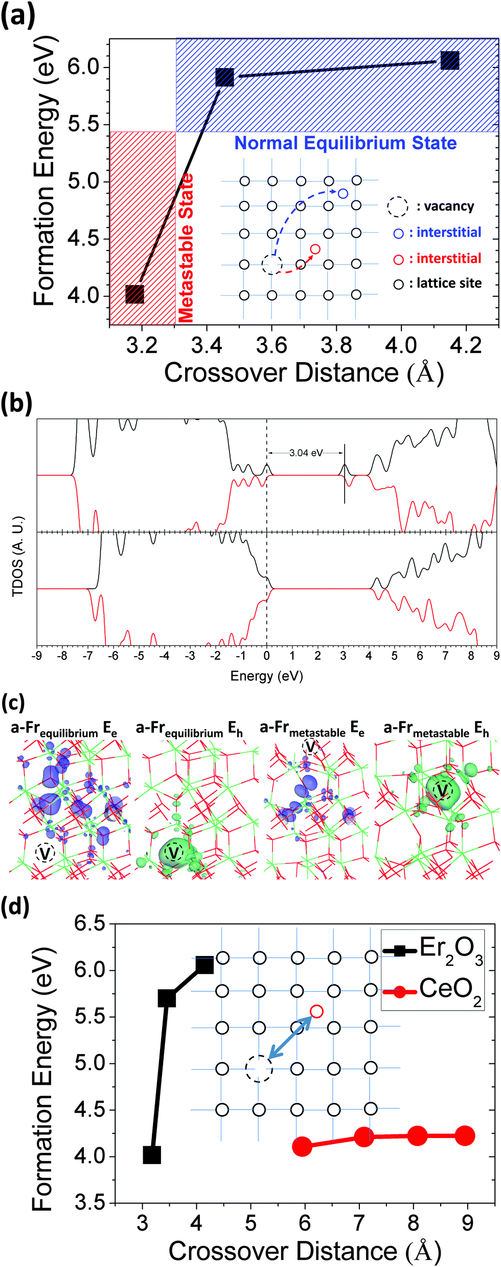
The anion Frenkel (a-Fr) defect is a common pair defect that is mostly formed by thermal fluctuations, which lead to the escape of one anion from its original site to an interstitial site trapped in the lattice. Thus, it always consists of a vacancy and an interstitial with charge neutrality. In fact, there is another prominent pair defect called the Schottky (STK) defect in the crystal lattice, which consists of a pair vacancy of a cation and anion. However, the STK defect is energetically favored in the simple cubic structure as demonstrated in our previous work,16 whereas the a-Fr defect is more favorable in the CaF2 (fluorite)-type structure. As supported by our defect formation energy, the neutral state of the STK defect (2VEr + 2VO4 + VO6)0 (i.e., a unit of A-type Er2O3) exhibits a formation energy of as high as 7.16 eV in the Er2O3 host lattice. Actually, Er2O3 can be treated as a distorted fluorite structure with broken symmetry; moreover, the radius of O is much smaller than that of Er. The a-Fr defect is a variable defect owing to the difference in crossover distance between the vacancy and the interstitial defect; furthermore, the coordination number of O required for creating the a-Fr defect is also different.Fig. 7(a) shows the formation energies, which are dependent on the crossover distance, of three typical a-Fr defects (VO + Oi) in Er2O3. We found that for crossover distances between 3.3 Å and 4.2 Å there is a normal equilibrium state for most a-Fr defects, because the Oi is sufficiently far away to escape the Coulomb attractive potential generated by the VO to prevent recombination and mutual annihilation. Another interesting state, which we called the metastable state, has a crossover distance of around 3.1–3.3 Å. The Oi remains at the cost of evident local site distortions to balance or screen the Coulomb attractive potential. From the formation energy, we see that the metastable O-related a-Fr defect is easy to form by external UV (∼250 nm) photoirradiation with an excitation energy of 4–5 eV and is stabilized by lattice distortions induced by thermal fluctuations. From Fig. 7(a), we found that the a-Fr defect in the metastable state has the lowest formation energy of 4.01 eV in total, which means about 2.0 eV per defect site. The formation energy of a-Fr is actually independent of the chemical potentials but relates to the lattice distortions due to ambient thermal fluctuations.
 | ||
| Fig. 7 (a) Dependence on the crossover distance of the formation energies of a-Fr defects. (b) TDOS of two typical a-Fr defects in neutral states. (c) Localized orbitals of electron and hole states produced by the two typical a-Fr defects (Er = green, O = red). (d) Comparison of the formation energy of the a-Fr pair defect vs. the crossover distance between Er2O3 and CeO2. | ||
Based on the formation energies of a-Fr within different charge states (−1, 0 and +1), we confirmed that a-Fr in both equilibrium and metastable states has a rather stable state at neutral charge in the mid-gap area. The a-Fr has a large positive value of Ueff (Ueff = +2.64 eV), and the neutral state that is stabilized with respect to the EF lies from EV + 0.77 eV (transition (0/+) for a-Fr) to EV + 3.41 eV (transition (−/0) for a-Fr) within the band gap area. Therefore, the reactions of O-related defects between various charge states are between deep levels that are generated by the neutral a-Fr.
Fig. 7(b) shows the single-particle levels (TDOS) of two typical states of the a-Fr defect in Er2O3. The upper panel shows the TDOS of the a-Fr within the equilibrium spatial extent (>3.3 Å). There are three localized p–π electronic states at the VB edge, which are similar to the states of Oi in the lattice. Another localized hole state lies 3.04 eV higher than the highest localized p–π level. In contrast, the metastable a-Fr only gives rise to a shallow p–π acceptor level close to the VBM, as shown in the lower panel of Fig. 7(b), and the hole state is 0.2 eV below the CBM. Fig. 7(c) shows the local orbitals of the gap states discussed above. The localized electronic states remain at the nearby distorted O sites of Oi, whereas the localized hole orbital surrounds the space left by VO. We made a further comparison of the formation energy of the a-Fr pair defect vs. the crossover distance between Er2O3 and CeO2, as shown in Fig. 7(d), as they have similar CaF2-type local symmetry; we see that Er2O3 exhibits a more drastic change in the distance of the a-Fr pair.
Pan et al. investigated the effects of oxygen vacancies in other lanthanide sesquioxides such as Lu2O3.67 They show that both oxygen vacancies and interstitials (non-lattice defects) are good charge carrier centers so as to enable filament conduction in Lu2O3.67 We similarly deduce that the oxygen-related defects play a similar role in Er2O3. This has gained support from the work of Chroneos et al.69 By their studies, it was found that all the sesquioxides favor the oxygen Frenkel pair defect (anion Frenkel, a-Fr), which is the lowest-energy mechanism of intrinsic lattice disorder in their calculations and summarizations. Stanek et al. have carried out further studies on the site preference of the sesquioxides and found that the lattice is less sensitive to such oxygen-related a-Fr pair defects.70 Therefore, in both the work of Stanek et al. and ours, these deductions are consistent with observations of the crystallography of these materials, which means that there is a high concentration of interstitial sites that exist in O sublattices, which are fully flexible to accommodate a large amount of oxygen defects.69 Moreover, a further experiment on an irradiation-induced order–disorder phase transformation in the sesquioxide Dy2O3 by Stanek et al.71 shows that the lattice will become disordered under a high-energy irradiation process, so as to provide a large amount of anion disorder or deficient defects in the disordered fluorite structure, and most of these defects result from the oxygen sublattice. This experiment provides supportive information for our model, in that a high-intensity laser beam will produce a large number of a-Fr pair defects within the host lattice in both ordered and disordered fluorite structures. In the process towards the equilibrium state, the a-Fr pair defects will become mobile enough to form a possible superlattice,71 which means that a potential transporting effect is provided by the a-Fr with the help of lattice disorder or vibrations.
Therefore, we similarly consider that oxygen-related defects, in particular a-Fr pairs, are the key intrinsic defects that have subtle effects on the practical optical properties of the host materials. They have a great potential to generate spurious emissions or low efficiencies of emissions in phosphor applications, owing to their property of trapping electrons or holes at O-related defect sites. Accordingly, a-Fr pair defects may play the role of charge-trapping sites that trap charge carriers, either electrons or holes, to limit or influence the luminescence performance.
Native defects-induced luminescence properties
An experiment reported persistent upconverted luminescence of Er2O3 under photostimulation at 975–980 nm (∼1.3 eV).14 A comparison was made between vacuum and ambient conditions, the only difference being the luminescence intensity. Persistent luminescence of Er2O3 has been discussed that was not related to extrinsic or intrinsic RE3+ ions. Therefore, the native point defects in this material play a significant role in modulating its luminescence properties. We summarize these native point defects in Table 1. Their thermodynamic transitions and single-particle levels are summarized in Fig. 8(a) and (b).| O-rich | Er-rich | O-rich | Er-rich | O-rich | Er-rich | ||||||
|---|---|---|---|---|---|---|---|---|---|---|---|
| VO6 | 0 | 7.40 | 0.05 | Oi | 0 | 2.16 | 10.12 | a-Fr meta | −1 | 12.53 | 12.53 |
| +1 | 3.31 | −4.04 | −1 | 4.55 | 12.50 | 0 | 4.01 | 4.01 | |||
| +2 | 0.22 | −7.13 | −2 | 6.48 | 14.43 | +1 | 5.86 | 5.86 | |||
| VO4 | 0 | 7.48 | 0.13 | VEr | 0 | 2.49 | 14.42 | Eri | 0 | 22.28 | 10.35 |
| +1 | 3.10 | −4.25 | −1 | 3.43 | 15.37 | +1 | 15.47 | 3.54 | |||
| +2 | −0.75 | −8.10 | −2 | 2.82 | 14.75 | +2 | 9.83 | −2.11 | |||
| −3 | 2.74 | 14.67 | +3 | 8.02 | −3.91 | ||||||
 | ||
| Fig. 8 (a) Summary of thermodynamic transition levels of different charge states of the intrinsic defects in Er2O3. The red lines denote donor-type transition levels and the black lines denote acceptor levels. (b) Summary of single-particle levels of the intrinsic defects in Er2O3 in different charge states (empty states = red, filled states = black). (c) F+-center model of luminescence. (d) Mechanism of luminescence related to native defects (N.D.) and dopant levels. The black line denotes the lengthened path of the optical transition for persistent luminescence, which is an intact “supply line” for electron transport. | ||
As we discussed above, there are many possible levels of native point defects that participate in or assist the process of luminescence. However, the key point for persistent luminescence is the release of energy at the activator site in the form of photons with energy transfer from the storage site. Therefore, we need to start with reactions of defect states for energy conversion during persistent luminescence. In contrast to other RE dopant-induced persistent luminescence in host materials, we introduce a model in which native point defects can be classified into two types, one acting as activators and the other being trap centers for energy storage. The most important point is to illustrate how electrons are driven by energy conversion for persistent luminescence. Here, we utilize the results of calculations on single-particle levels and thermodynamic transition levels (ionization energy) to elucidate our models.
For the process of persistent luminescence, we give an interpretation of the experimental results in the following way.
There are two possible mechanisms of luminescence, as illustrated in Fig. 8(c) and (d): one is related to F+ centers, the other is related to energy conversion between defects. It has been discussed that oxygen vacancies formed with +Ueff are usually color centers.24 V+O6 and V+O4 are the so-called F+ centers in Er2O3. The energy intervals between localized electron and hole levels in the band gap are about 1.3 eV, by which electrons can be stimulated from the occupied levels in the band gap into the CB or near the CB edge via the localized hole states (EV + 4.46 eV for V+O6, EV + 4.93 eV for V+O4, EV = VBM) in which the excited electrons are accommodated. The localized occupied levels for electrons that were mentioned lie at 3.30 eV and 3.67 eV for V+O6 and V+O4, respectively. An excited electron at the CB edge is relatively unstable compared with its defect-related states in the band gap; therefore, it will be de-excited back to its original ground-state levels at EV + 3.30 eV for V+O6 and EV + 3.67 eV for V+O4, respectively, and the energy released in the form of photons with energies of 2.21 eV (561 nm) and 1.82 eV (681 nm), respectively. The experimentally reported NIR emission is about 1540 nm owing to the de-excitation of electrons from the CB edge to the localized level for V2+O4. The energy difference between this state and the CB edge is about 0.7 eV (1770 nm), which is of the correct magnitude compared with the experimental results.14 According to analysis based on the F+-center model (Fig. 8(c)), the experimentally reported twin peaks are attributed to the de-excitation of excited electrons back to the localized electron level within the band gap in the ground state for such defects. The lower luminescence band (535 nm) seems to correspond to de-excitation at the V+O6 site and the higher band (660 nm) at the V+O4 site, respectively. The paths of the excitation and de-excitation of electrons are illustrated by the blue, pink and purple lines in Fig. 8(c).
However, this model seems to be inconsistent with the phenomenon observed in experiments. An experiment compared luminescence between vacuum and ambient conditions.14,72,73 The twin peak observed at 565 nm was found to be evidently weakened in ambient conditions compared with the peak found in a vacuum. We noted that the sample used in the experiment was a powder of nanoparticle size. As we know, nanoparticles have large surface-to-volume ratios; therefore, types of O vacancy dominate the entire luminescence of the particle. Oxygen has low coordination numbers on the upper surface owing to structural truncation compared with the bulk. On exposure to air, a surface with O vacancies with low coordination numbers is covered or terminated by H2O molecules so as to quench the related luminescence. The other luminescence peak is attributed to O vacancies with high coordination numbers found in the bulk. A recent experiment on persistent luminescence shows a further comparison for the luminescence at 1540 nm between vacuum and ambient conditions; a similar weakening effect was found in ambient conditions, which means a reduction in the transition from V2+O4 to V2+O6.14 Because the peak position is unchanged, it is therefore a reduction in the levels induced by VO4. Based on this discussion, the F+-center model of persistent luminescence has been ruled out.
Another, different mechanism is a model of energy conversion relating to different defects that react mutually between different charge states so as to accomplish the energy transfer for luminescence. Therefore, in this model, we not only refer to the reactions of charge states in a given defect, but also discuss the reactions of inter-defects through different evolutions of charge states from the point of view of energy. In Fig. 8(d), the blue, pink and purple lines denote the possible paths of the excitation and de-excitation of electrons, which correspond to absorption and emission in luminescence spectroscopy. The two major differences from the F+-center model are that the native point defects provide upconversion levels for electrons that are continuously stimulated from the VB into the localized defect levels in the gap and that, secondly, the luminescence is the release of energy in terms of photons among the reactions of different defects between various charge states, instead of single defect sites between different charge states.
Luminescence occurs with the transfer of electrons between the deep levels near the mid-gap area, as demonstrated by the following reactions of defects in the form of two-electron processes:
 | (2) |
 | (3) |
| V2+O + O2−i → (a-Fr)metastable + Ueff5 | (4) |
Taking into consideration the image charge corrections for charged states of point defects, the effective correlation energies for these related two-electron reactions of defects are Ueff1 = −3.91 eV, Ueff2 = −4.48 eV, Ueff3 = −1.77 eV, and Ueff4 = −3.31 eV, respectively, which show that the reactions are uniformly exothermic. The two electrons in these reactions will overcome the repulsive Coulomb potentials to become correlated to form a doubly occupied site, i.e. O2−i, as a result of the negative Ueff. Hence, the energies that are released per electron from each of the defect reactions above are 1.95 eV, 2.24 eV, 0.88 eV, and 1.65 eV, respectively. We studied a luminescence experiment with peak values of 660 nm, 535 nm, 1540 nm, and 825 nm. Hence, our predicted energies can be shown as wavelengths if they are released in terms of photons: 635 nm, 554 nm, 1402 nm, and 749 nm with mean relative errors (MREs) of 4%, −3%, 9%, and 9%, respectively. Considering that an acceptable error is 50% from the experimental measurements made by Tanner et al.,14 we confirm that the predictions from our second model (the energy conversion model) show good consistency. According to this analysis, the wavelengths of the luminescence centers predicted by the energy conversion model not only exhibit the correct physical and chemical trends but also have relatively low errors. Based on discussions of the second model, we deduce that the short-wavelength limit of the emission spectra observed in the experiment on persistent luminescence14 is contributed by the energy converted by electron transfer from V+O4 to the Oi sites. After eqn (2) and (3) complete the reactions, the final products, i.e. V2+O and O2−i, are converted back into the a-Fr in the metastable state, as the a-Fr is about 2.68 eV lower than the energy of V2+O + O2i; therefore, Ueff5 = −2.68 eV.
This can be confirmed from the single-particle levels as summarized in our TDOS calculations in Fig. 8(d). Electrons are excited by near-infrared (NIR) photostimulation with a photon energy of 975–980 nm (∼1.3 eV). A many-photon process will assist the electrons to move from the valence band into the levels of the native point defects and then into the localized defect levels provided by V+O6 and V+O4, and the electrons that are originally from the valence band can be easily exchanged with the lowest occupied electron levels via thermal fluctuations within the range of 30–100 meV. The electrons will be further excited into the conduction band via a two-photon excitation process using NIR photostimulation at 980 nm (1.3 eV). As is known, Er3+-related solids are widely employed in the field of optical communications owing to their unique emission at 1.54 μm.74 Compared with other Ln3+ ion-related solids, Er3+-related solids are preferred because of their highly quantum-efficient two-photon upconversion process.75 Actually, from Fig. 3(a) of ref. 14, the slope of the relationship between the power and the emission intensity shows that the process is a two-photon upconversion with a value of the slope of about 2.2 for measurements under vacuum conditions. Measurements in air show that about 0.8 photons are involved, which nearly approaches 1, and a one-photon process in air has also been confirmed from our transition levels.
These electrons are relatively unstable and will be de-excited spontaneously back to the closest localized defect levels provided by V2+O6 and V2+O4, as shown in Fig. 8(d). These levels are localized hole states and only accommodate these de-excited electrons for a short time (several ns); then, the electrons will finally be accepted/trapped by the deep localized levels provided by O−i sites. The O−i sites will be converted back into rather stable states in the form of O2−i deep in the gap and transfer these electrons back to the occupied localized electron levels provided by O2−i sites. Afterwards, these electrons complete the entire local transport cycle back to the top of the VB because there are three localized electron levels for O2−i sites with intervals of about 0.2–0.3 eV and the lowest localized electron levels are only about 0.15 eV higher than the top of the VB. To enable the existence of O−i, it can be possible to create a number of O−i sites locally in Er2O3 temporarily by optical excitation such as NIR photostimulation. From the optical aspect, with continuous excitation of the higher-energy absorption band, the electron paramagnetic resonance (EPR)-active spin-1/2 state O−i further increases in concentration when temporarily generated. The reactions shown in eqn (2) and (3) will cause quenching of this state via a rapid transition reaction of this defect, 2O−i → O0i + O2−i, as it has a negative Ueff as discussed in the section on O interstitials. Therefore, the Oi is the essential activator site and the luminescent state is its EPR-active spin-1/2 state O−i, which is locally generated by temporary NIR photostimulation. With electron–hole recombination and the release of the energy in terms of photons, this luminescent state will revert to the O2−i state to transfer the electrons back to the VB of the host material.
According to our energy conversion model, we have made further efforts to generalize this model and explain the mechanism of persistent luminescence together with its photoelectron dynamics in terms of physical chemistry. Inspired by the radiation decay of the visible and invisible rays studied by Becquerel in 1896, we have transferred this mechanism of radiation decay to model our persistent luminescence, as they are similar to some extent: the emission of rays is the release of energy due to the transfer of electrons between different levels within an atom (radiation decay) or solid particles (persistent luminescence), respectively.
As shown in Fig. 9(a), we have here established a conversed chain reaction (CCR) scheme to reinforce our energy conversion model that is related to native defects, because we believe that this CCR scheme is a more general mechanism compared with the abovementioned reactions of native defects, as the native point defects are intermediates that assist in the operation of this mechanism. The reason why we have considered CCR is because the abovementioned reactions of native point defects in different charge states are exothermic processes that are accomplished within a short timescale that is similar to that of the lattice vibrations, and the final product of each cycle is the same as the initial reactant if we consider eqn (2)–(4).
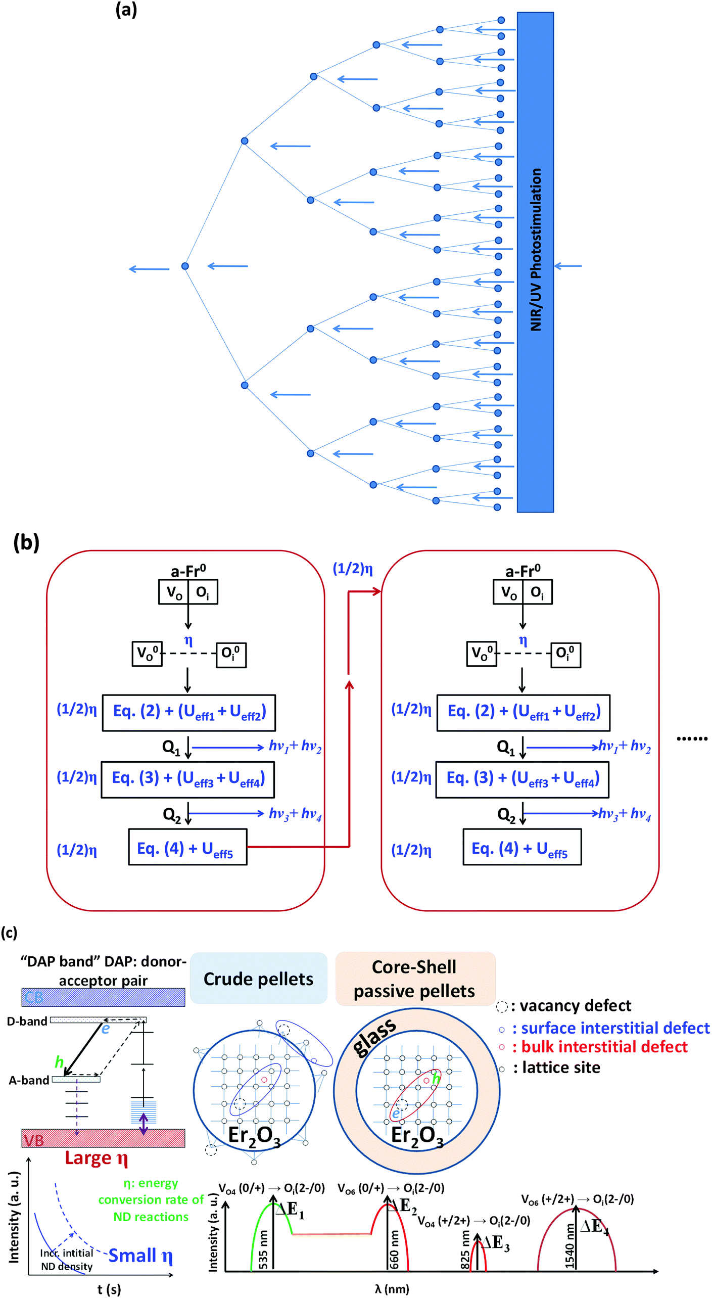 | ||
| Fig. 9 (a) Schematic diagram of the conversed chain reaction showing the energy conversions. (b) Detailed schematic process of energy conversion within a group of native point defects between different charge states. (c) A passive core–shell model is suggested to enhance the formation of a DAP band (DAP: donor–acceptor pair), so as to quench the emission at the short-wavelength limit for a red phosphor. | ||
Fig. 9(b) shows a schematic process of energy conversion. In each new chain reaction cycle, the concentration of the reactants is actually a reduced concentration of the products from the previous cycle. Therefore, we assume that there is a possibility η, which represents the efficiency of energy conversion per second, that a-Fr pair defects separate from each other into neutral states (V0O and O0i). We neglect the effect of temperature in the Arrhenius equation, the value of η is nearly constant for a given material as an intrinsic property based on the synthesis conditions, and the entire reaction process together with energy conversion is confirmed as being based on a more complicated reaction model than a first-order chemical reaction. We mark each cycle based on the time in seconds. According to our modeling, the rate of the reaction may not be linearly dependent on the reactant concentration at that moment:
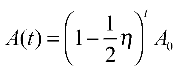 | (5) |
Only when η is a very small constant (0 < η ≪ 1) do we get an approximation that is similar to the first-order reaction rate equation shown as follows:
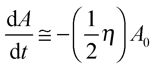 | (5a) |
In an obvious relationship, the number of photons generated is proportional to the concentration of a-Fr defects at each moment in time. Then, regardless of the approximation from eqn (5) and (5a), the number of photons generated by the CCR at a time t is shown exactly as:
 | (6) |
If we simply assume that the emission intensity is proportional to the number of photons, this allows IPL(t) ∝ Nphoton(t). Thus, the spectrum of the decay of persistent luminescence can be simulated by an equation based on eqn (6):
 | (7a) |
We find that the behavior of eqn (7a) is very similar to that in experiments on persistent luminescence.12–14,19Eqn (5)–(7a) all represent special cases of luminescence with multiple peaks and between different charge states, which is due to O vacancies having the effect of a positive Ueff. For persistent luminescence with a single peak and a −Ueff for O defects eqn (7a) is generalized as eqn (7b):
| IPL(t) = (η)tIPL(0) and t1/2 = ln2/(−lnη) → single-peak PL | (7b) |
We see that the half-life is actually an intrinsic property of given materials that exhibit persistent luminescence. Considering both of the above cases, an increase in the value of η is the key factor that prolongs the duration of persistent luminescence. Otherwise, it is also possible to increase the initial intensity of luminescence by merely increasing the defect concentration, so as to increase the duration of persistent luminescence by rigidly shifting up the emission decay curve. It is highly technically demanding to increase the value of η, which is essential for prolonging the intrinsic persistent luminescence of a given material. It is advisable to increase the defect concentration and reduce the activation barrier to defect reactions. Usually, sintering is a popular method for increasing the defect concentration by means of increasing the density of materials via a more densely packed structure, which has been reported in other experiments.76–79 Another possible way to create neutral pair defects in a state of thermal disequilibrium is by using external stress, which can provide a similar effect to sintering.80–84
According to the experiment on the persistent luminescence of Er2O3 by Tanner et al.,14 we see that the decay of the emission at 660 nm has a half-life of about 0.25 s, whereas this is about 0.625 s for the decay at 1540 nm. Using eqn (7a), the values of η are found to be 0.125 (or 12.5%) for 660 nm and 0.660 (66.0%) for 1540 nm in vacuum conditions. This means that the rates of conversion from a-Fr to V0O + O0i are 12.5% and 14.4% in ambient air conditions (i.e.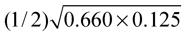 ) for the processes shown in eqn (2) and (3). Our energy conversion modeling shows consistent results, in that the luminescence intensity is higher at 1540 nm than the case at 660 nm owing to the energy conversion efficiency being higher.
Conclusion
We have investigated the mechanism of the intrinsic persistent luminescence of Er2O3 in the A-type lattice based on first-principles calculations. Particular attention has been paid to the native point defects, thermodynamic transition levels and single-particle levels in terms of their electronic properties and formation energies. The native point defects are engaged in mutual subtle interactions in the form of chemical reactions between different charge states. The release of energy related to lattice distortion facilitates the conversion of energy for electrons to be transported between the valence band and the trap levels or even between the deep trap levels so as to generate persistent luminescence.In the A-type lattice of Er2O3, we chose 4- and 6-fold coordinated VO to model this type of defect via low and high coordination numbers of VO in real materials. At the Er-rich limit (or O-poor chemical potential limit), we found that both V0O4 and V0O6 have nearly the same lowest energies with values of 0.13 eV and 0.05 eV, which indicates that high-coordination VO is energetically favored in Er2O3. Both are deep donors with a +Ueff and the charge state transitions and single-particle levels remain deep near the mid-gap region. At the O-rich limit, the neutral Oi is the dominant defect with a formation energy of as low as 2.16 eV and it has a −Ueff of −0.45 eV. The VEr acts as a shallow acceptor with a transition level (3−/0) that is only 0.08 eV higher than the VBM, and it has a relatively low formation energy of 2.49 eV in the same O-rich conditions with a rather high negative −Ueff. For the lattice distortion defect a-Fr, we found two categories of state, equilibrium and metastable, which correspond to different ranges of the crossover distance for such pair defects. The metastable type has 4.01 eV per pair (i.e. 2.01 eV per defect site), whereas the value is 6.06 eV per pair for the equilibrium state. Eri in the triply positive state is relatively stable in Er2O3 because it has a negative formation energy at the Er-rich limit, and its deep donor transition level (2+/3+) is 1.8 eV higher than the VBM. Except for VEr, nearly all of these native point defects have deep thermal transition levels that are related to EF near the mid-gap region.
An experiment has observed three different bands of persistent luminescence in the emission spectrum, which are located at 535 nm (green), 660 nm (red), and 1540 nm (NIR).14 We ruled out the F+-center model of luminescence for persistent luminescence because comparative experiments on both ordinary upconversion luminescence and persistent phosphors between ambient air and vacuum conditions show quenching of the optical transition owing to the termination by water vapor of low-coordinate VO sites.14,72 A model of energy conversion has been established to explain the electron transport between different trap levels that supplies the energy to transfer and maintain the observed dynamics of persistent luminescence. Our calculations on the thermodynamic transition levels confirm that both visible and NIR experimentally observed intrinsic persistent luminescence (phosphor or afterglow) are related to the thermodynamic transition levels of O-related defects, and the thermodynamic transition levels within different charge states for these defects are independent of the chemical potentials of the given species. The lowest peak (short-wavelength limit) in the persistent luminescence band is contributed by the transition levels of charged donor–acceptor recombination between (0/+) of V0O4 and (2−/0) of Oi, in which the excited electrons and emitted photons exactly follow the zero-phonon lines, because the mutual local lattice relaxation effects of these pair defects counteract each other. In this way, similar physical and chemical trends show that the red luminescence (intermediate) is generated by the transitions between (0/+) of V0O6 and (2−/0) of Oi, whereas the persistent luminescence in the NIR region is provided by the levels between VO4 and VO6, as summarized in Fig. 9(c).
We have further established a conversed chain reaction (CCR) model to interpret the energy conversion process of persistent luminescence in terms of the inter-reactions of native point defects between different charge states. It is advantageous to use the study of defect levels combined with that of formation energies to suggest limits to doping energy and explain photostimulated luminescence in terms of native point defects.
Acknowledgements
The author gratefully acknowledges the support of the Natural Science Foundation of China (NSFC) for the Youth Scientist grant (Grant No. NSFC 11504309) and the initial start-up grant support from the Department General Research Fund (Dept. GRF) from ABCT in the Hong Kong Polytechnic University.References
- K. Van den Eeckhout, P. F. Smet and D. Poelman, Materials, 2010, 3, 2536 CrossRef CAS.
- K. Van den Eeckhout, D. Poelman and P. Smet, Materials, 2013, 6, 2789 CrossRef CAS.
- P. F. Smet, I. Moreels, Z. Hens and D. Poelman, Materials, 2010, 3, 2834 CrossRef CAS.
- J. Hölsä, Electrochem. Soc. Interface, 2009, 18, 42 Search PubMed.
- T. Aitasalo, P. Dereń, J. Hölsä, H. Jungner, J. C. Krupa, M. Lastusaari, J. Legendziewicz, J. Niittykoski and W. Strk, J. Solid State Chem., 2003, 171, 114 CrossRef CAS.
- T. Matsuzawa, Y. Aoki, N. Takeuchi and Y. Murayama, J. Electrochem. Soc., 1996, 143, 2670 CrossRef CAS.
- F. Liu, W. Yan, Y.-J. Chuang, Z. Zhen, J. Xie and Z. Pan, Sci. Rep., 2013, 3, 1554 Search PubMed.
- T. Maldiney, et al. , Nat. Mater., 2014, 13, 418 CrossRef CAS PubMed.
- Z. Pan, Y.-Y. Lu and F. Liu, Nat. Mater., 2012, 11, 58 CrossRef CAS PubMed.
- A. Abdukayum, J.-T. Chen, Q. Zhao and X.-P. Yan, J. Am. Chem. Soc., 2013, 135, 14125 CrossRef CAS PubMed.
- Z. Li, Y. Zhang, X. Wu, L. Huang, D. Li, W. Fan and G. Han, J. Am. Chem. Soc., 2015, 137, 5304 CrossRef CAS PubMed.
- D. C. Rodriguez Burbano, E. M. Rodriguez, P. Dorenbos, M. Bettinelli and J. A. Capobianco, J. Mater. Chem. C, 2014, 2, 228 RSC.
- D. C. Rodríguez Burbano, S. K. Sharma, P. Dorenbos, B. Viana and J. A. Capobianco, Adv. Opt. Mater., 2015, 3, 551 CrossRef.
- J. Wang, J. H. Hao and P. A. Tanner, J. Lumin., 2015, 164, 116 CrossRef CAS.
- P. A. Tanner, Chem. Soc. Rev., 2013, 42, 5090 RSC.
- B. Huang, Inorg. Chem., 2015, 54, 11423 CrossRef CAS PubMed.
- B. Huang, R. Gillen and J. Robertson, J. Phys. Chem. C, 2014, 118, 24248 CAS.
- B. Huang, Philos. Mag., 2014, 94, 3052 CrossRef CAS.
- T. Maldiney, A. Lecointre, B. Viana, A. Bessière, M. Bessodes, D. Gourier, C. Richard and D. Scherman, J. Am. Chem. Soc., 2011, 133, 11810 CrossRef CAS PubMed.
- A. De Vos, K. Lejaeghere, D. E. P. Vanpoucke, J. J. Joos, P. F. Smet and K. Hemelsoet, Inorg. Chem., 2016, 55, 2402 CrossRef CAS PubMed.
- S. Z. Karazhanov and P. Ravindran, J. Am. Ceram. Soc., 2010, 93, 3335 CrossRef CAS.
- T. Zhai, X. Fang, M. Liao, X. Xu, H. Zeng, B. Yoshio and D. Golberg, Sensors, 2009, 9, 6504 CrossRef CAS PubMed.
- Z. Łodziana and J. Piechota, Phys. Rev. B: Condens. Matter Mater. Phys., 2006, 74, 184117 CrossRef.
- B. Qu, B. Zhang, L. Wang, R. Zhou and X. C. Zeng, Chem. Mater., 2015, 27, 2195 CrossRef CAS.
- K. Huang and A. Rhys, Proc. R. Soc. London, Ser. A, 1950, 204, 406 CrossRef CAS.
- P. Kaipa and F. Lüty, Phys. Rev. B: Condens. Matter Mater. Phys., 1985, 32, 1264 CrossRef CAS.
- J. R. Weber, W. F. Koehl, J. B. Varley, A. Janotti, B. B. Buckley, C. G. Van de Walle and D. D. Awschalom, Proc. Natl. Acad. Sci. U. S. A., 2010, 107, 8513 CrossRef CAS PubMed.
- B. Huang and J. Robertson, Phys. Rev. B: Condens. Matter Mater. Phys., 2012, 85, 125305 CrossRef.
- B. Huang and J. Robertson, J. Non-Cryst. Solids, 2012, 358, 2393 CrossRef CAS.
- B. Huang, Phys. Status Solidi B, 2015, 252, 431 CrossRef CAS.
- G.-y. Adachi and N. Imanaka, Chem. Rev., 1998, 98, 1479 CrossRef CAS.
- R. Gillen, S. J. Clark and J. Robertson, Phys. Rev. B: Condens. Matter Mater. Phys., 2013, 87, 125116 CrossRef.
- H. Jiang, R. I. Gomez-Abal, P. Rinke and M. Scheffler, Phys. Rev. Lett., 2009, 102, 126403 CrossRef PubMed.
- H. Jiang, P. Rinke and M. Scheffler, Phys. Rev. B: Condens. Matter Mater. Phys., 2012, 86, 125115 CrossRef.
- K. Xiong and J. Robertson, Appl. Phys. Lett., 2009, 95, 022903 CrossRef.
- J. Robertson, Eur. Phys. J.: Appl. Phys., 2004, 28, 265 CrossRef CAS.
- J. Robertson, J. Appl. Phys., 2008, 104, 124111 CrossRef.
- S. J. Clark, M. D. Segall, C. J. Pickard, P. J. Hasnip, M. I. J. Probert, K. Refson and M. C. Payne, Z. Kristallogr., 2005, 220, 567 CAS.
- C. J. Pickard, B. Winkler, R. K. Chen, M. C. Payne, M. H. Lee, J. S. Lin, J. A. White, V. Milman and D. Vanderbilt, Phys. Rev. Lett., 2000, 85, 5122 CrossRef CAS PubMed.
- T. Zacherle, A. Schriever, R. A. De Souza and M. Martin, Phys. Rev. B: Condens. Matter Mater. Phys., 2013, 87, 134104 CrossRef.
- P. R. L. Keating, D. O. Scanlon, B. J. Morgan, N. M. Galea and G. W. Watson, J. Phys. Chem. C, 2011, 116, 2443 Search PubMed.
- B. Huang, J. Comput. Chem., 2016, 37, 825 CrossRef CAS PubMed.
- (a) B. Huang, Solid State Commun., 2016, 230, 49 CrossRef CAS; (b) B. Huang, Solid State Commun., 2016, 237–238, 34–37 CrossRef.
- P. J. Hasnip and C. J. Pickard, Comput. Phys. Commun., 2006, 174, 24 CrossRef CAS.
- K. Laasonen, A. Pasquarello, R. Car, C. Lee and D. Vanderbilt, Phys. Rev. B: Condens. Matter Mater. Phys., 1993, 47, 10142 CrossRef CAS.
- A. M. Rappe, K. M. Rabe, E. Kaxiras and J. D. Joannopoulos, Phys. Rev. B: Condens. Matter Mater. Phys., 1990, 41, 1227 CrossRef.
- L. Kleinman and D. M. Bylander, Phys. Rev. Lett., 1982, 48, 1425 CrossRef CAS.
- S. G. Louie, S. Froyen and M. L. Cohen, Phys. Rev. B: Condens. Matter Mater. Phys., 1982, 26, 1738 CrossRef CAS.
- I. Grinberg, N. J. Ramer and A. M. Rappe, Phys. Rev. B: Condens. Matter Mater. Phys., 2000, 62, 2311 CrossRef CAS.
- N. Marzari, D. Vanderbilt and M. C. Payne, Phys. Rev. Lett., 1997, 79, 1337 CrossRef CAS.
- M. I. J. Probert and M. C. Payne, Phys. Rev. B: Condens. Matter Mater. Phys., 2003, 67, 075204 CrossRef.
- I. A. Vladimir, F. Aryasetiawan and A. I. Lichtenstein, J. Phys.: Condens. Matter, 1997, 9, 767 CrossRef.
- S. Lany and A. Zunger, Phys. Rev. B: Condens. Matter Mater. Phys., 2009, 80, 085202 CrossRef.
- S. Lany and A. Zunger, Phys. Rev. B: Condens. Matter Mater. Phys., 2010, 81, 205209 CrossRef.
- B. J. Morgan and G. W. Watson, J. Phys. Chem. C, 2010, 114, 2321 CAS.
- S. Lany and A. Zunger, Phys. Rev. B: Condens. Matter Mater. Phys., 2008, 78, 235104 CrossRef.
- S.-i. Kimura, F. Arai and M. Ikezawa, J. Phys. Soc. Jpn., 2000, 69, 3451 CrossRef CAS.
- A. V. Prokofiev, A. I. Shelykh and B. T. Melekh, J. Alloys Compd., 1996, 242, 41 CrossRef CAS.
- E. J. Huber, E. L. Head and C. E. Holley, J. Phys. Chem., 1956, 60, 1582 CrossRef CAS.
- L. R. Morss, P. P. Day, C. Felinto and H. Brito, J. Chem. Thermodyn., 1993, 25, 415 CrossRef CAS.
- B. Wu, M. Zinkevich, F. Aldinger, D. Wen and L. Chen, J. Solid State Chem., 2007, 180, 3280 CrossRef CAS.
- L. Gerald, M. Leonardo and B. Karen Paz, Jpn. J. Appl. Phys., 2011, 50, 04DA15 CrossRef.
- S.-P. Gao, J. Jiang, M. Cao, J. Zhu and J. Yuan, Phys. Rev. B: Condens. Matter Mater. Phys., 2004, 69, 214419 CrossRef.
- K. Xiong, J. Robertson, M. C. Gibson and S. J. Clark, Appl. Phys. Lett., 2005, 87, 183505 CrossRef.
- F.-H. Chen, J.-L. Her, Y.-H. Shao, Y. H. Matsuda and T.-M. Pan, Nanoscale Res. Lett., 2013, 8, 1 CrossRef PubMed.
- X. J. Zheng, L. He, Y. C. Zhou and M. H. Tang, Appl. Phys. Lett., 2006, 89, 252908 CrossRef.
- S. Mondal, J.-L. Her, K. Koyama and T.-M. Pan, Nanoscale Res. Lett., 2014, 9, 1 CrossRef PubMed.
- S. Lany and A. Zunger, Phys. Rev. B: Condens. Matter Mater. Phys., 2005, 72, 035215 CrossRef.
- A. Chroneos, M. R. Levy, C. R. Stanek, K. McClellan and R. W. Grimes, Phys. Status Solidi C, 2007, 4, 1213 CrossRef CAS.
- C. R. Stanek, K. J. McClellan, B. P. Uberuaga, K. E. Sickafus, M. R. Levy and R. W. Grimes, Phys. Rev. B: Condens. Matter Mater. Phys., 2007, 75, 134101 CrossRef.
- M. Tang, P. Lu, J. A. Valdez, C. R. Stanek and K. E. Sickafus, Phys. Status Solidi C, 2007, 4, 1171 CrossRef CAS.
- J. Wang, J. H. Hao and P. A. Tanner, Opt. Express, 2011, 19, 11753 CrossRef CAS PubMed.
- P. Tanner, in Lanthanide Luminescence, ed. P. Hänninen and H. Härmä, Springer, Berlin Heidelberg, 2011, vol. 7, p. 183 Search PubMed.
- H. Sulaiman Wadi, T. Nizam, P. Prabakaran and A. Harith, Jpn. J. Appl. Phys., 2002, 41, L332 Search PubMed.
- F. Auzel, Chem. Rev., 2004, 104, 139 CrossRef CAS PubMed.
- D. A. Pejaković, J. Lumin., 2010, 130, 1048 CrossRef.
- J. Zhang, Z. Zhang and T. Wang, Chem. Mater., 2004, 16, 768 CrossRef CAS.
- P. G. Baranov, N. G. Romanov, D. O. Tolmachev, C. de Mello Donegá, A. Meijerink, S. B. Orlinskii and J. Schmidt, JETP Lett., 2006, 84, 400 CrossRef CAS.
- A. S. Gurin, N. G. Romanov, D. O. Tolmachev and P. G. Baranov, Phys. Solid State, 2015, 57, 280 CrossRef CAS.
- D. Tu, C.-N. Xu, Y. Fujio and A. Yoshida, Light: Sci. Appl., 2015, 4, e356 CrossRef CAS.
- J.-C. Zhang, L.-Z. Zhao, Y.-Z. Long, H.-D. Zhang, B. Sun, W.-P. Han, X. Yan and X. Wang, Chem. Mater., 2015, 27, 7481 CrossRef CAS.
- H. Zhang, D. Peng, W. Wang, L. Dong and C. Pan, J. Phys. Chem. C, 2015, 119, 28136 CAS.
- X. Wang, et al. , Adv. Mater., 2015, 27, 2324 CrossRef CAS PubMed.
- D. Peng, B. Chen and F. Wang, ChemPlusChem, 2015, 80, 1209 CrossRef CAS.
| This journal is © the Owner Societies 2016 |