
 Open Access Article
 This Open Access Article is licensed under a Creative Commons Attribution-Non Commercial 3.0 Unported Licence
Hydrogen on silicene: like or unlike graphene?
Michele
Pizzochero†
a,
Matteo
Bonfanti
a and
Rocco
Martinazzo
*ab
aUniversitá degli Studi di Milano, Dipartimento di Chimica, via Golgi 19, 20133 Milano, Italy. E-mail: rocco.martinazzo@unimi.it
bConsiglio Nazionale delle Ricerche, Istituto di Scienze e Tecnologie Molecolari, Milano, Italy
First published on 11th May 2016
Abstract
Hydrogenation of free-standing silicene, the two-dimensional allotrope of silicon, is investigated in detail using first-principles methods and compared with the adsorption of H atoms on graphene. Similarly to graphene, chemisorption of a single H atom on silicene induces the formation of a semilocalized state around the adatom, a sharp peak in the density of states at the Fermi level which acts as a strong resonant scatterer for charge carriers. This state hosts an unpaired electron, the itinerant electron of the resonating valence bond picture which primarily resides on the “majority” sublattice and biases the reactivity towards specific lattice positions. Contrary to graphene, sticking of hydrogen atoms is barrierless, on both the pristine and the hydrogenated surface. As a consequence, hydrogen adsorption on silicene is expected to proceed randomly under typical laboratory conditions, and preferential binding to form balanced dimers (or clusters) only occurs when thermodynamic equilibrium conditions prevail. The absence of clustering can be experimentally confirmed using scanning tunneling microscopy techniques since simulated imaging shows that the investigated structures provide distinguishable features that should allow their easy identification, if present on the surface. Overall, our findings can be rationalized by the fact that in silicene π bonds are weaker and the lattice is softer than in graphene and suggest that in silicene adatoms may severely limit carrier mobility.
1 Introduction
The isolation of graphene in 2004,1 along with the determination of its magneto-optical properties,2–6 revolutionized the field of condensed matter science. Besides many other things, this discovery triggered a wealth of fundamental and applied studies on other atomic-thick two-dimensional (2D) materials. The search of new 2D materials started from those which could be peeled off from natural crystals (e.g. BN, MoS2, MoSe2, WS2, WSe2, NbSe2, NiTe2, Bi2Se3, Be2Te3 and black phosphorus) through either mechanical7 or chemical exfoliation,8 and rapidly evolved into the synthesis of novel layered materials. This goal was first accomplished in 2012 when compelling evidence for silicene, the two-dimensional allotrope of Si, was reported.9 Since then, a new gold rush for group IV elemental analogues of graphene (beside silicene, germanene and stanene) has started, as well as the search for other (group III, V) elemental compounds (e.g. boronene and phosphorene) with unexplored characteristics. The fabrication of van der Waals bound heterostructures, layer-by-layer, is largely considered to be the ultimate strategy to assemble new materials with desired properties.10Among elemental 2D systems, silicene has attracted much attention from the community since the beginning, mainly because of the expectation of being easily integrated into the existing Si-based technology.11 Like its analogues germanene and stanene, silicene features a sizable spin–orbit coupling (SOC) which makes the spin Hall effect observable at ordinary temperatures and opens a mini-gap of ∼1.6 meV in the band electronic structure.12,13 The spin Hall effect and the gap opening are not trivial, since they turn silicene into a topological material (insulator) with helical edges.14
Several different phases of silicene have been reported on the hexagonal Ag single crystal surface and, more recently, on ultra-thin Ag(111) films, ZrB2(0001), Ir(111) and MoS2(0001) (see ref. 11 for a recent review). The different phases have varying superlattice structure with respect to the underlying substrate (e.g., on Ag(111), a number of 4 × 4,  ,
,  and
and  phases have been reported, and the
  phases are still debated and most likely appropriate for bilayer and few-layer silicene) and differ only in the buckling pattern.‡ “Buckling” of the surface is a feature common to most of the known 2D materials – with the notable exception of graphene and h-BN, they are not really one-atom-thick, rather show some atoms in the unit cell vertically displaced from the others. Although this property signals some kind of structural instability with respect to a flat arrangement of the atoms, it may turn to be advantageous for applications. In silicene, such a buckling allows the two sublattices to be distinguished when applying an electric field along the surface normal, thereby opening a sizable band gap and eventually triggering a topological phase transition of the electronic structure.14–16 Similarly for chemical functionalization, which can be used to break the reflection symmetry and induce an out-of-plane dipole polarization and piezoelectricity.17 The bucking height (closely related to a mixed sp2–sp3 hybridization of the Si atoms in the sheet) can be modified by stretching the sheet, thereby suggesting that the spin–orbit coupling and the ensuing electronic properties might be mechanically controlled to some extent; in graphene, for instance, the sp3-like lattice protrusions created by adsorbing hydrogen atoms were shown to dramatically affect the SOC, both theoretically18,19 and experimentally.20 Importantly, silicene field effect transistors have already been fabricated and operated for a few minutes, despite their limited stability in air.21 Though mainly a proof-of-concept, these exciting experiments promise to be a big twist in the field and pave the way to overcome the known limitations of graphene for digital electronic applications.
Many different kinds of chemical functionalization have been proposed for silicene, including hydrogenation,22–25 halogenation26–29 and oxidation.30 Silicane, the fully hydrogenated sheet analogue to graphane, has been predicted to have a band-gap in the range 2.9–3.8 eV, depending on the configuration,23 and is thus potentially useful for optoelectronics in the blue/violet energy range. Intermediate hydrogenation of a silicene bilayer has been theoretically proved to provide exceptional optoelectronic properties, and various structures have been proposed for solar applications and for illumination as white light emitting diodes.25 Half-silicane was predicted to be a ferromagnet with a Curie temperature of about 300 K24 and has been recently obtained on the Ag(111) surface upon hydrogenating the  phase, along with (more stable) defective areas with one, two and three holes in the superlattice unit cell.31 The same authors of ref. 31 previously reported32 a partially hydrogenated silicene superstructure with a H/Si ratio of 7/18 on the 4 × 4 phase on Ag(111), thereby showing that different hydrogenated phases can be obtained on the same substrate depending on the target silicene phase. In turn, these studies highlight the delicate interplay between the silicene–substrate interactions and the kinetics of the adsorption process.
In this paper we investigate in detail the hydrogenation process of a free-standing sheet – a prototypical example of adsorption of monovalent species – as a first step to understand more complex behaviors which are expected (and observed) when silicene is grown on a substrate. Although silicene sheets, which are “suspended” or grown on an inert substrate, have not been synthesized yet, progress in this direction appears to be desirable for electronic applications. Hence it is important to theoretically investigate such issues in advance and make a thorough comparison with the analogous process on free-standing graphene, for which a rather rich scenario emerged in the last ten years or so, joining together as diverse phenomena as charge- and spin-transport, magnetism and chemistry.33–35 Some previous studies already dealt with the hydrogenation of silicene, either free-standing or variously supported,22–25,31,36–43 but a well-rounded perspective – one that encompasses the appearance and role of adatom-induced electronic states, their impact on charge transport and on adatom clustering, the presence of energy barriers to sticking, and the magnetic properties of the defective substrate – is missing. We fill this gap in the rest of the paper by sequentially analyzing the electronic and structural properties of the pristine substrate, the single H atom adsorption event and the ensuing midgap state, the formation of dimers and of some more hydrogenated structures. Importantly, we further show that the investigated hydrogenated structures can be clearly distinguished using scanning tunneling microscope (STM) techniques.
The paper is organized as follows. The computational set-up is described in Section 2, our findings are introduced and discussed in Section 3 and, finally, Section 4 summarizes and concludes.
2 Computational details
All our first-principles calculations were performed within the pseudopotential, spin-polarized density functional theory (DFT) framework, as implemented in the periodic, atomic-orbital based SIESTA code,44 using the gradient-corrected exchange–correlation functional devised by Perdew, Burke and Ernzerhof (PBE)45,46 to describe exchange and correlation effects. The Kohn–Sham orbitals for the valence electrons were represented as linear combinations of numerical, atom-centered basis functions of triple-ζ plus polarization (TZP) quality whereas core electrons were replaced by norm-conserving pseudopotentials47 including partial core corrections.48Silicene layers were described by hexagonal supercells [na1,na2] ( , i = 1, 2 being the primitive lattice vectors of silicene and a0 its lattice constant, a0 ≈ 3.8 Å), but several n × m supercells of the rectangular unit [a1 + a2, a2 − a1] were also considered to investigate intermediate impurity concentrations that cannot be achieved with the conventional supercell. A large vacuum layer of ca. 14 Å was introduced along the surface normal (here and in the following the z-axis) to avoid artificial interactions between periodic images, and integrations over the Brillouin zone (BZ) were carried out on a Γ-centered k-mesh following the Monkhorst–Pack scheme.49 Geometry optimizations used the equivalent of a 30 × 30 × 1 (30 × 18 × 1) k-point mesh for the hexagonal (rectangular) unit cell of silicene, and finer grids were used for the calculation of the density of states (DOS) (150 × 150 × 1), and for the phonon- and energy-dispersion curves (80 × 80 × 1), the latter with hexagonal supercells only. Atomic coordinates were fully relaxed until the forces were smaller than 0.01 eV Å−1 and cell optimizations used a stringent threshold on the maximum component of the stress tensor (1 MPa), together with a large mesh cutoff of 400 Ry for the real-space integration of the charge-density to prevent any egg-box effect. The mesh cutoff was later increased to 800 Ry when investigating single-H adsorption energetics.
Before investigating the reactivity of silicene toward hydrogenation, the stability of the substrate was checked by computing the whole phonon dispersion using the small displacement technique. A 5 × 5 hexagonal supercell was adopted to ensure appropriate convergence of the dynamical matrix elements over the lattice sum, and the atomic displacement along each direction was set to 0.04 Bohr.
3 Results and discussion
3.1 Free-standing silicene
For completeness we briefly summarize here our findings for the structure, the stability and the electronic properties of the pristine substrate. These represent a set of well established results (see ref. 11 and references therein) which allow us to validate the adopted computational approach and to highlight similarities and differences with graphene, at the same level of theory that was used for the hydrogenation process discussed below.Silicon atoms in silicene are packed in a honeycomb lattice with a Si–Si bond length of 2.282 Å and a lattice constant of 3.854 Å. Unlike graphene, the two equivalent sublattices of which silicene is made up lay at different heights, resulting in a buckling height (the relative position of the sublattices along the surface normal) of 0.506 Å. This is the so-called low buckled configuration; a higher buckled structure with a much smaller lattice constant (∼2.7 Å) exists but it is stable only when enforcing hexagonal symmetry.50,51
It is a fascinating question whether Si atoms in silicene are involved in a sp2 rather than in a sp3 hybridization. In fact, the non-planar geometry could be associated with sp3 arrangement, whereas the honeycomb lattice characterized by three equivalent bond lengths – which is peculiar of graphitic materials – suggests sp2 hybridization. sp2-like hybridization was argued from reflection electron energy loss spectroscopy of silicene on a silver substrate,52 but ruled out in any silicon nanostructure from theoretical considerations.53 A mixed sp2–sp3 hybridization was demonstrated using Raman spectroscopy,51 and this interpretation agrees with the results of our first-principles calculations since we found a Si–Si–Si angle of 115°, which is intermediate between 120° of sp2 systems and 109.5° of sp3 ones.
Closely related to this issue is the nature of the π electron network, what made graphene so fascinating to trigger much of the recent research in materials science. Strictly speaking, the occurrence of true π bonds requires the planar symmetry of the substrate. This is not the case of silicene and therefore we refer to the Si–Si bonds as to quasi-π bonds, i.e. bonds which are (much) weaker than true π-bonds because of the reduced overlap between pz orbitals. The weakening of the “π-bonds” is best seen by comparing the stability of buckled silicene with that of graphene, as shown in Fig. 1 which reports the results of constrained lattice optimizations performed for several values of the buckling height (i.e. the optical Z-mode at the Γ point). For a graphene flake, the break of planar symmetry implies the weakening of the π bond. Therefore, the energy quickly increases when buckling the structure. For silicene, in contrast, some buckling stabilizes its structure and, moreover, further buckling causes a slow increase only of its energy. These opposite situations are evident from the energetics: for graphene, a displacement of one atom along the direction normal to the surface of a few tenths of Å implies an energy increase of several eV; the same displacement for silicene, from its equilibrium geometry, leads to a destabilization of only some tens of meV. The different strengths of chemical bonding can also be grasped from the small cohesive energy of silicene, which we found to be 4.65 eV per atom, compared with the value of 8.79 eV per atom appropriate to graphene.54
 | ||
| Fig. 1 Buckling energy (per unit cell) in silicene (left panel) and graphene (right panel), referenced to the planar structures, as a function of the relative displacement ΔZ of the height of the atoms in the unit cell. Note that the energy scale in the right panel is 20 times larger than in the left panel. | ||
The reason for this behavior can be traced back to the concept of “π-capability”.55 Both carbon and silicon atoms exhibit a ground-state s2p2 electronic configuration that is responsible for their peculiar chemistry. However, the energy separation between s and p valence orbitals§ is larger for C than Si. As a consequence, silicon tends to use all the p orbitals when it hybridizes, i.e. to live in sp3 (or sp3-like) environments, whereas carbon admits intermediate hybridizations, hence a rich chemistry with sp, sp2 and sp3 arrangements.
Buckled and planar silicenes share essentially the same band structure, which is also the same as graphene. In fact, from the energy dispersions shown in the left panel of Fig. 2, one can observe that the valence and conduction bands cross in a linear fashion at the corners of the Brillouin zone (the K, K′ points). The main difference between graphene and silicene electronic structure lies in the relative position of their σ and π bands, which are closer to each other in silicene, on account of the smaller s–p separation mentioned above. This is clearly seen from the highest-energy occupied electronic levels close to the Γ point: in both planar silicene and graphene they describe σ bonds but in silicene they lie only ∼2 eV below the Fermi level. Furthermore, upon buckling, these energy levels are those subjected to the largest change, and the upward shift in energy supports the idea of a partial rehybridization (from pure sp2 to something intermediate between sp2 and sp3).
 | ||
| Fig. 2 Electronic band structure (left panel) and phonon dispersion (right) along the high-symmetry path Γ–M–K–Γ of the BZ, for both the buckled and the planar silicene structures (solid and dashed lines, respectively). In the left panel the Fermi level is set to zero, and in the right panel the imaginary frequencies have been placed on the negative frequency axis. | ||
Although planar and low buckled silicenes have quite similar total energy and electronic properties, their vibrational properties are very different, as a consequence of the instability (stability) of the former (the latter) toward buckling. In Fig. 2, right panel, we show the phonon dispersion of low buckled silicene. Looking along the Γ–M path, the branches are, in the order of increasing frequencies, the out-of-plane (“ZA”) flexural mode and the longitudinal and transverse acoustical modes (LA, and TA, respectively), and their corresponding optical counterparts, namely the out-of-plane, the transverse and longitudinal optical modes (ZO, TO and LO, respectively). In M the LO and TO branches are found at ∼450 cm−1 and ∼500 cm−1, respectively, i.e. at much lower values than in graphene (1340.52 and 1398.6 cm−1, respectively58); the ZO branch, on the other hand, has a much lower frequency (ω ∼ 100 cm−1 in M) and mixes with LA as a consequence of the surface buckling. Similarly for the doubly degenerate mode at the zone center (of symmetry E2g in D3d) at about ω ∼ 550 cm−1 which is the only active Raman mode and in graphene is responsible for the well-known G peak at 1580 cm−1. For comparison, notice that in a graphene lattice with the mass of Si the latter value would be ω = 1034 cm−1, an indication that the silicene lattice is indeed much softer than graphene.
Obviously, planar silicene shows a large imaginary branch around Γ which makes the planar structure unstable toward ZO, i.e. the out-of-plane optical mode which buckles the structure and confers some sp3 character to the system.59
3.2 Adsorption of a single H atom
For H adsorption on graphene, it was demonstrated that both the size of the binding energy and the extent of the sheet puckering strongly depend on the surface coverage.60 Thus, as a starting point, we fully relaxed several supercell structures, ranging from 1 × 1 to 9 × 9, that correspond to an adatom concentration Θ varying from 0.50 ML to 0.006 ML (the monolayer ML is here defined to have one H atom per Si atom, i.e. Θ = nH/nSi where nH(nSi) is the number of H (Si) atoms in the unit cell). We define the binding energy as Echem = Ehost + EH − EH+host, where EH+host and Ehost are the energies of the substrate with and without an additional H adatom, respectively, and EH is the energy of an isolated hydrogen atom. We corrected the Basis Set Superposition Error (BSSE) using the popular a posteriori counterpoise (CP) method.61 Additionally, we estimated the lattice distortion energetics upon chemisorption by means of the surface reconstruction energy Esurf, which is defined as the difference in energy between the relaxed hydrogenated silicene structure freed from the adatom and its pristine counterpart.When the hydrogen atom impinges on the surface, a covalent Si–H interaction can be formed only if a Si–Si quasi-π bond breaks and a re-hybridization of the bonding Si atom to true sp3 configuration takes place. This has deep consequences on the geometrical structure around the adsorbate: the Si–Si bond length stretches from ∼2.28 Å to ∼2.39 Å and the hydrogenated Si atom moves out of the surface plane by further ∼0.28 Å to take part in a covalent bond with the approaching atom, which is ∼1.51 Å long. A Si–Si–H angle of 110° results, which is very close to the value expected in an ideal tetrahedral arrangement. These results depend only weakly on the supercell size, as a quick look at the “puckering” height and at the surface reconstruction energy reported in Table 1 reveals. From that table, one further concludes that the binding energy of a hydrogen atom to silicene is 2.16 eV, again with a weak dependence on the supercell size and in sharp contrast to graphene, where the binding energy of a H atom is ∼0.8 eV.60,62,63 Our energetics is in excellent agreement with previous reports64,65 and well converged with respect to computational parameters. Similar results concerning the stability of H atoms on the Si sheet were obtained when looking at the diffusion barriers:66 at a similar theory level the lowest energy diffusion barrier Ed was found to be 0.73 eV, that is large compared to H on typical transition metal surfaces67 but yet smaller than Echem above. This finding is again in sharp contrast to graphene where Ed matches the desorption energy.68 In other words, while H adatoms on graphene are immobile and desorb rather than diffusing, on the silicene sheet they can move along the surface.
| Supercell | Θ (ML) | E chem (eV) | E surf (eV) | δZ (Å) |
|---|---|---|---|---|
| 1 × 1 | 0.500 | 2.147 | 0.065 | 0.083 |
| 2 × 2 | 0.125 | 2.228 | 0.095 | 0.236 |
| 3 × 3 | 0.056 | 2.177 | 0.086 | 0.290 |
| 4 × 4 | 0.031 | 2.173 | 0.094 | 0.263 |
| 5 × 5 | 0.020 | 2.172 | 0.102 | 0.270 |
| 6 × 6 | 0.014 | 2.162 | 0.097 | 0.274 |
| 7 × 7 | 0.010 | 2.167 | 0.106 | 0.280 |
| 8 × 8 | 0.008 | 2.161 | 0.110 | 0.286 |
| 9 × 9 | 0.006 | 2.165 | 0.111 | 0.287 |
Activation barriers play a crucial role in predicting the chemisorption process, from the very first adsorption event to the formation of overlayers with some finite coverage. Hereto, we delved deeper into the Si–H bond formation by investigating the adsorption profile of a H atom impinging on the silicon sheet. We investigated the energetics along an adsorption profile that mimicked the minimum energy path, namely following the trajectory of a hydrogen atom approaching the surface along the direction normal to the layer, on the top of a silicon atom. We used a 4 × 4 supercell, keeping the Si–H bond length frozen at a number of selected values and relaxing the remaining atomic coordinates. As is shown in Fig. 3, we found out that H chemisorption on silicene is a barrierless process, again in sharp contrast to H adsorption on graphene, for which a barrier to sticking ∼0.2 eV high was found.54,60
 | ||
| Fig. 3 Counterpoise corrected adsorption profile of a H atom sticking on the upward displaced (left panel) and downward displaced (right panel) Si atom in silicene (circles joined by solid lines). Also shown for comparison are the energy values uncorrected for the BSSE (dashed lines). | ||
These differences between silicene and graphene are mainly due to two distinct, though somewhat related, effects. Firstly, π bonds in graphene are stronger than in silicene, which is also the ultimate reason why sp2 hybridization is stabilized in graphene. This is manifested in the larger bandwidth of the graphene electronic structure, see for instance the much larger splitting at the M point of the BZ (∼6 eV in graphene, to be compared with ∼2 eV from Fig. 2) or, equivalently, the position of the plasmon peak in the (experimentally accessible) absorptive component of the optical conductivity. That is, the average position of the π and the π* bands points toward a stronger bond in graphene, i.e. a larger energy for those π* ← π transitions which are involved in the process of bond breaking. This is a consequence of the joint effect of the strength of each π bond and of the delocalization energy gain, both related to the value of the hopping energy between neighboring pz orbitals (∼3.0 eV in graphene and ∼1.1 eV in silicene13). More rigorously, the strength of the π bonds can be quantitatively estimated from the energy of the lowest-lying triplet excitations, i.e. as the energy required to create a pair of non-bonding electrons from the sea of electrons in the ground (fully bound) state. This energy can be computed in standard (ground-state) DFT calculations with fixed magnetization, a special case of the so-called ΔSCF method. The size of the supercell used fixes the spatial extent of the magnetic excitation (a magnon) or, equivalently, determines the value q of the magnon momentum at which the excitation energy ε(q) is obtained. The limit q → 0 is in principle required but for comparative purposes we can limit ourselves to the calculation of the excitation energy in a relatively large supercell. We used a 12 × 12 supercell and found ε = 0.694 eV for graphene and ε = 0.217 eV for silicene, a rather marked difference between the two substrates.
Secondly, the surface reconstruction energy is smaller for silicene than for graphene, i.e. the former is a much softer substrate because of the weaker π and σ bonds that the Si atoms form in the sheet. Furthermore, pristine silicene is “naturally” characterized by a buckling of 0.51 Å, whereas free-standing graphene is completely planar. Therefore, the adjustment of the substrate atom height upon hydrogen binding is smaller for silicene (0.274 Å) than for graphene (0.529 Å). In general, the whole structural rearrangement is of smaller extent in the silicon flake. The Si–Si bond length around the adsorbate elongates by 4.86%, whereas in graphene the C–C bond undergoes a more significant stretching of 5.21% (1.418 Å → 1.496 Å). Apart from these details, the lattice distortions accompanying adsorption are very similar for both the carbon and the silicon sheet, with the same deformation pattern in the two cases, only slightly longer ranged for graphene. This is made clear in Fig. 4, which reports the strain fields generated by the adatom on both substrates, and clearly shows the elongation of the bonds closest to the adatoms and the shrinking of the next closest bonds.
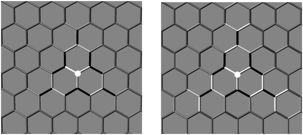 | ||
| Fig. 4 Defect-induced strain fields for silicene (left panel) and graphene (right panel), as obtained from calculations on a rectangular 7 × 7 supercell. White balls represent hydrogen atoms. Colors vary from black to white for increasing bond lengths in the range [0.995,1.005] ×deq where deq is the equilibrium bond length of each pristine sheet. | ||
The main difference between graphene and silicene is in the out-of-plane distortion, again related to the strength of the π bonds. For a graphene flake, pulling out a C atom from the plane implies the loss of substantial aromaticity, at least around the lifted atom. In contrast, pristine silicene already presents protrusions along the direction normal to the surface, making the formation of a tetrahedral geometry easier. Thus, the difference in reconstruction is due to the contrasting tendency of these monolayers to take the hydrogenated atom out of the layer upon chemisorption, which is stronger in silicene. In light of this, it is not surprising that the reconstruction energy of the surface upon hydrogenation is only ∼0.1 eV (see Table 1) for silicene, i.e. one order of magnitude smaller than that in graphene (∼1.0 eV).60
The reconstruction energy Esurf can also be used to estimate the binding energy of a hydrogen atom on a “prepared” (protruded) atom of the lattice, i.e. Echem* = Echem + Esurf ≈ (2.1 + 0.1) eV in silicene and Echem* ≈ 1.8 eV in graphene. Echem* can roughly be interpreted as the energy freed from the coupling of the two unpaired electrons (one of the adsorbate and one of the lattice), reduced by the energy needed to completely break a double π in the distorted configuration. Assuming that the former depends only weakly on the substrate, as it seems reasonable, the larger value of Echem* found for silicene is a further confirmation of the weaker π bonds in this system.
We further investigated the effect of the lattice distortion along the normal to the surface by also considering the chemisorption of a H atom at the other sublattice, namely the one downward displaced. For this case it is clear that a larger displacement of the hydrogenated silicon atom is necessary in order to form a Si–H bond, and we found it to be 1.11 Å. As a consequence, the surface reconstruction energy increases up to 0.528 eV. Nevertheless, the counterpoise-corrected binding energy is 2.035 eV, i.e. rather similar to that for adsorption at the pushed-out-silicon. This is in agreement with the behavior represented in Fig. 1. The lack of pure π-interactions implies, contrary to graphene, a non-rigid structure, and therefore the large displacement of the Si atom which is necessary to bind the hydrogen turns out to have a minor effect on the chemisorption energetics. In fact, adsorption remains barrierless despite unfavorable structural effects (Fig. 3, right panel).
Finally, we analyzed the effect that hydrogen adsorption has on the electronic structure of the substrate. It is well known that the adsorption of an atom forming a strong covalent bond with a carbon site of a graphitic surface deeply affects the electronic properties of the substrate.2,5,60,69 This is a consequence of the (approximate) bipartite nature of the lattice and of the sublattice imbalance generated by the adsorption process. In fact, a number of “midgap” states at least equal to the sublattice imbalance – and which localizes on the majority sublattice – are expected in this situation from a simple counting rule, the so-called “imbalance rule” (see e.g.ref. 63 and references therein). For adsorbed species the imbalance arises when the adsorbate–surface bond is strong enough that the pz orbital of the site is effectively removed from the π cloud, i.e. in the so-called unitary limit where adatoms behave like vacancies. In the case of a honeycomb lattice with an isolated impurity of this kind, it was shown theoretically,70,71 and confirmed experimentally,72 that the midgap state ψ is semi-localized around the defect position, and, though not normalizable, it has a characteristic dependence ψ ∼ 1/r on the distance r from the defect. This state hosts the itinerant electron appearing in the resonating valence bond picture of the adsorption process60 and describes a paramagnetic center with a local magnetic moment μ = 1 μB (where μB is the Bohr magneton) uncoupled from the π conducting states.73
Silicene behaves similarly to graphene in this respect, since the above results translate unchanged in the honeycomb silicene lattice. As a consequence, the density of states of hydrogenated silicene shows, similar to graphene, two peaks symmetrically placed around the Fermi level (Fig. 5, left panel), which then describe a singly occupied midgap state with a magnetic moment of 1 μB. Interestingly, in the case of silicene the computed magnetic moment rapidly drops to zero when increasing the supercell size (Fig. 5, right panel), thereby signaling that the exchange (RKKY) interaction between the (periodically repeated) moments is smaller in silicene than in graphene. In fact, in the simulated periodic arrangements of H adatoms the computed moment is the result of a delicate balance between two opposing effects. On the one hand, there is the exchange interaction that favors the maximum (ferromagnetic) coupling between moments, as predicted by Lieb's theorem74 for electrons on bipartite lattices with short-range interactions.¶ On the other hand, there is a tendency to doubly occupy the slightly dispersive impurity-induced bands. The exchange interaction determines the splitting (Δ) between the spin-majority and the spin-minority peaks in the DOS, whereas the dispersion of the impurity-induced band(s) determines the intrinsic widths (Γ) of the midgap peak(s) (Fig. 5, left panel). For silicene Δ ≪ Γ already on a 10 × 10 supercell, and thus the electronic structure becomes unpolarized (non-magnetic) approximately above this supercell size.||
 | ||
| Fig. 5 Left panel: Density of states for a hydrogen adatom in a 6 × 6 silicene supercell, with the spin majority (minority) component on the positive (negative) axis. Also shown for comparison as red lines is the DOS of the pristine system. Energy is referenced to the Fermi level (vertical dashed line). Right panel: Magnetic moment μ as a function of the inverse of the hydrogen atom coverage ΘH. Rhombi (squares) represent magnetic moments obtained in a hexagonal (rectangular) supercell. Also displayed, for comparison, are the results for graphene (stars). | ||
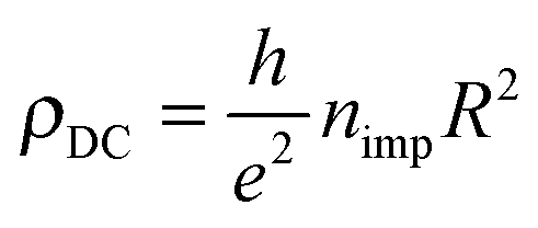
It is worth noticing in this context that the above sharp peaks in the density of states have important consequences on charge transport in graphene, and the same occurs for silicene too. In graphene the sharp (midgap) states induced by adatoms (and carbon atom vacancies) form strong, “resonant” scattering centers which give rise to a quasi-linear dependence of the extrinsic graphene's conductivity on the carrier density (or gate voltage), as observed experimentally.2,4,5 When the substrate–adatom bond is sufficiently strong (or when the defect is a vacancy) the behavior is universal – i.e. it does not depend on the details of the chemical species attached to the sheet – and the contribution of the resonant scatterers to the DC resistivity takes the form2,5,35
Reverting the question around, if resonant scatterers are indeed the main factors limiting the charge transport in these 2D materials, the measured mobilities can be used to estimate the adatom concentration. Using the expression above for ρDC at a density of 2 × 10¹¹ charge carriers per cm2 [n ≈ 5 × 10⁻⁵, corresponding to a gate potential of few volts in a typical gated configuration using a ∼300 nm thick layer of SiO2 as dielectrics], we may write the mobility as
| μ = 1.93 × nimp−1 × cm2 V−1 s−1 |
![[thin space (1/6-em)]](https://www.rsc.org/images/entities/char_2009.gif) 000 cm2 V−1 s−1) and nimp ∼ 2 × 10⁻² for silicene samples obtained so far21 (μ ∼ 100 cm2 V−1 s−1).††
000 cm2 V−1 s−1) and nimp ∼ 2 × 10⁻² for silicene samples obtained so far21 (μ ∼ 100 cm2 V−1 s−1).††
3.3 Dimers
The changes in the electronic structure of the substrate mentioned at the end of the previous section have important consequences on the adsorption process. Indeed, it was shown that in graphene the localization of the midgap state (and the ensuing magnetization) on the majority sublattice biases reactivity towards specific lattice positions60 and this explains the preferential sticking observed experimentally.68 Since the electronic properties remain (qualitatively) unchanged when passing from graphene to silicene it is instructive to consider this issue in the case of silicene.To this end we investigated the adsorption of a second hydrogen atom as a function of the distance from the first H adatom, placed on an upward displaced Si sublattice site, at a number of neighboring sites illustrated in Fig. 6. The resulting trend in the binding energies is shown in Fig. 6, along with the behavior of the Mulliken site-magnetizations in the singly hydrogenated silicene sheet. The latter are defined as the difference between spin-up and spin-down Mulliken populations of the given sites and, analogously to the site-integrated magnetization introduced in ref. 60, measure the unpaired electron density available for coupling (binding) with the H electron.
 | ||
| Fig. 6 Top panel: Investigated adsorption sites for hydrogen dimer formation on a 6 × 6 supercell. Yellow balls represent silicon atoms, with the first H placed at A0. Middle panel: Binding energy (Echem) for a second H atom as a function of the distance from the first H adatom. Bottom panel: Mulliken site-magnetizations (q) in the singly hydrogenated silicene sheet. Sites at which adsorption occurs are labeled according to the top panel. The thick red line represents the binding energy of the first H atom. | ||
From Fig. 6 one can observe the following. Firstly, adsorption near the defect (in the so-called ortho position) is strongly favored. Binding to this site is about half an eV stronger than on the pristine surface. Secondly, it can be clearly noticed that, if the first H atom is chemisorbed on a given sublattice (A in Fig. 6), the second atom preferentially binds at the opposite sublattice (B in Fig. 6), thereby forming dimers of “AB” type. Secondary adsorption at the A sublattice is characterized by the same energetics of the first H atom (with only minor differences of the order of 1 meV), while adsorption at the B sublattice is favored, increasingly more when moving closer to the first H atom position. These findings parallel those found on graphene, though with a less marked sublattice dependence than in graphene.60
In general, there are two driving forces that act in orienting the stability of the second adatom, namely (i) structural and (ii) electronic effects. Table 2 shows the surface puckering and the reconstruction energy upon H binding for the ortho, meta and para dimers (i.e. secondary adsorption at the B0, A1 and B2 sites, respectively), for both the syn- (same face) and the anti- (opposite faces) configurations. Focusing on the former, which are most relevant when adsorption occurs on a supported sheet, from a purely structural viewpoint one can argue that the meta dimer might be the most stable isomer. The reconstruction energy accompanying hydrogenation at this site is the lowest among all the dimers, as a consequence of the intrinsic buckling of the silicene sheet. The heights of Si atoms in the meta position are very close to that in pristine silicene (0.56 Å vs. 0.51 Å) and this implies that reconstruction energies are similar as well (0.10 eV vs. 0.11 eV). Therefore, it is not surprising that the chemisorption energy at this site is very close to that for the first H atom adsorption, with only a minor difference of about 20 meV. One can say that the chemistry of the meta site is mainly governed by the weak structural effect induced by first adatom, and thus no significant differences with the binding of a single H on pristine silicene is observed. A similar situation occurs for any site in the same sublattice as that occupied by the first hydrogen atom, where adsorption energetics remains very close to the single hydrogen case. Electronic effects are at work in ortho and para dimers which, despite the unfavorable structural arrangement, turn out to be the most stable configurations. Hence, electronic effects overcome structural instabilities in these two cases. The same holds for compact “AB” dimers, up to some large values of the H–H distance (∼18 Å, see B5 data point in Fig. 6) where structural effects start to dominate the overall energetics.
| Configuration | E chem (eV) | δZ (Å) | E surf (eV) | μ (μB) |
|---|---|---|---|---|
| syn-o-A0B0 | 2.605 | 1.190 | 0.403 | 0.00 |
| syn-m-A0A1 | 2.185 | 0.296 | 0.105 | 1.87 |
| syn-p-A0B1 | 2.470 | 1.065 | 0.414 | 0.00 |
| anti-o-A0B0 | 2.877 | 0.152 | 0.080 | 0.00 |
| anti-m-A0A1 | 2.075 | 1.163 | 0.539 | 1.63 |
| anti-p-A0B1 | 2.675 | 0.267 | 0.105 | 0.00 |
As mentioned above, the electronic effects arise because of facile pairing between the electron of the approaching H atom and the unpaired electron semilocalized on the lattice around the first H, as described by the midgap state appearing in the electronic structure of singly hydrogenated silicene or, equivalently, by the ensuing spin-density. Therefore, the computed binding energies correlate well with the Mulliken site-magnetizations of the singly hydrogenated sheet, as shown in Fig. 6 (bottom panel). Secondary adsorption on the A sublattice (where no unpaired electron density resides) necessarily breaks an additional quasi-π bond, that is adsorption proceeds similarly to the hydrogenation of pristine silicene, modulated by minor structural effects. In contrast, the chemisorption on the B sublattice (where the unpaired electron resides, with a probability that decays as ∼1/r2 from the first H position) leads to facile pairing and bond formation between the electron lying on the surface and the one coming from the approaching atom.
In accordance with the above picture, one expects no magnetism for H pairs adsorbed on opposite sublattices (AB dimers) and magnetic configurations when the second H atom binds at the same sublattice (A2 dimers). This is confirmed by our first principles calculations, where a non-vanishing magnetic moment (of ∼1.9 μB) is found for meta dimers only (see Table 2). This behavior is also reflected in the density of states reported in Fig. 7 for the ortho-, meta- and para-dimers, which show a spin-polarized solution for the meta case and unpolarized solutions otherwise. Interestingly, it can be clearly seen in Fig. 7 that the DOS of the ortho- and para-cases shows broadened but yet visible resonances at about ±0.4 eV from the Fermi level which arise from the mixing of the two midgap states related to the H atoms, whereas no real mixing occurs in the meta-case. This is due to the fact that in the first case the midgap states localize in opposite sublattices – hence are subjected to strong coupling through nearest-neighbor hoppings – whereas in the latter case they localize on the same sublattice – hence they are “protected” by the vanishingly small value of the second-neighbor hoppings. This is nothing but the imbalance rule stated above, in the more realistic situation where electron–hole symmetry is only approximate.
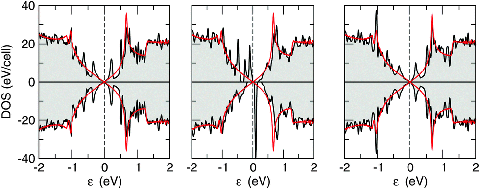 | ||
| Fig. 7 Density of states for (left) ortho, (middle) meta and (right) para dimers computed on a 6 × 6 supercell (black lines). Red lines represent the DOS of the pristine substrate, for comparison. Energies are referenced to the Fermi level (vertical dashed lines). | ||
In addition, one can notice that ortho dimer formation is 130 meV more exothermic than the para counterpart, in agreement with the decay of the spin density (Fig. 6) and similar to what happens in graphene. Differently from graphene, we find that any adsorption path is barrierless like that for the first hydrogen atom. In the case of graphene, while an energy barrier for forming meta dimers had to be expected on general grounds (i.e. the similarity to the first adsorption process), the presence of a barrier in forming ortho dimers could only be explained by structural (steric) effects.60 In silicene, structural effects play a minor role and no steric hindrance appears when adsorbing H atoms on neighboring sites.
In general, the lack of activation barriers for adsorption represents a marked difference between hydrogen sticking on silicene and on graphene. In the latter case, activated adsorption in unfavored sites enables adsorption to be under kinetic control under typical (cold plasma) laboratory conditions, and allows preferential sticking forming AB dimers to easily manifest itself.60,68 In silicene, the adsorption rate has the same high value for any site – the one expected for barrierless sticking – only the desorption rate depends on the strength of the surface–atom bond. In other words, the preferential binding to specific lattice positions only appears in thermodynamic equilibrium, when the silicene surface is left to equilibrate with an atomic-hydrogen gas at some fixed pressure. If equilibrium is not achieved, hydrogenation of silicene is a rather random process, without any clustering tendency of the adatoms, in sharp contrast to graphene.
Finally, Table 2 also shows some energetic and structural aspects of double-sided hydrogenation. It is instructive to consider this case too, since electronic effects do not depend on the facial selectivity and structural effects can be easily singled out in this case. A close inspection of these findings suggests a symmetrical situation between syn and anti pairs. In fact, the surface reconstruction energy (Esurf) is minimal for the meta dimer in the syn-arrangement and for both the ortho- and para-, anti-dimers, all with Esurf ∼ 0.1 eV. Conversely, Esurf is about four times larger than this value for both the same-sublattice opposite-faces case (A2-anti) and for the opposite-sublattice same-face one (AB-syn). This behavior is easily rationalized by recalling that in silicene, contrary to graphene, the two sublattices lay at different heights, hence they bind hydrogen atoms preferentially on the face from which they stand out. On combining structural with electronic effects one finds that the ortho–anti-dimer is by far the most stable isomer, about 370 meV more stable than its syn counterpart. The optimized structures of these configurations are shown in Fig. 8 where one can notice that the syn H pair requires a much larger lattice distortion to “invert” the protrusion and accommodate the second adatom at the ortho-site.
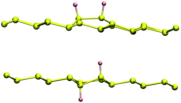 | ||
| Fig. 8 Relaxed structure of the ortho–syn (top panel) and ortho–anti (bottom panel) dimers. | ||
3.4 Trimers
As a final subject of investigation, we studied the adsorption of a third hydrogen atom on silicene, i.e. the formation of trimers. As a starting structure we considered the case in which the first two H adatoms bind at different sublattices on the same face of the surface in their most stable configuration, i.e. ortho dimers. The number of possible sites to consider is very large, therefore we just sketch the picture on the basis of the representative set of adsorption sites shown in Fig. 9.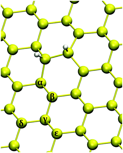 | ||
| Fig. 9 Investigated chemisorption sites for triple hydrogenation on a 6 × 6 supercell. Yellow (white) balls represent silicon (hydrogen) atoms. | ||
As discussed in the previous section, ortho dimers are non-magnetic (i.e. they lack unpaired electrons) since adatoms sit on different sublattices. Therefore, when adding a third hydrogen atom the main effect to consider is structural, i.e. the lattice distortion induced by the two adsorbates. Furthermore, breaking of a Si–Si quasi-π bond is necessary in order to form a covalent interaction, and thus magnetism arises again.
Looking at Table 3, two different cases can be recognized: (a) when the binding energy of the H atom is equal to or larger than the chemisorption energy of the first hydrogen atom (i.e. α, γ and ε sites) and then (b) the cases in which adsorption is less exothermic than the first H atom (i.e. β and δ). Chemisorption at α and ε sites are the easiest to achieve due to the height of the binding Si atom: just a small displacement (∼0.4 Å) in the direction out of the layer is necessary to reach a sp3 hybridization and form a chemical bond with hydrogen. On the other hand, for β and δ silicon atoms, hydrogenation is unfavorable due to the significant puckering (∼1.2 Å) these atoms have to undergo to form a Si–H bond. These opposite behaviors emerge in the value of Esurf: for the (b) configurations the surface reconstruction is very large if compared with (a) cases (∼0.12 eV) and therefore hydrogenation is not expected to occur at β and δ sites from a thermodynamic point of view.
| Site | E chem (eV) | Z (Å) | δZ (Å) | E surf (eV) | μ (μB) |
|---|---|---|---|---|---|
| α | 2.502 | 0.711 | 0.411 | 0.128 | 0.84 |
| β | 2.130 | 0.092 | 1.214 | 0.378 | 0.96 |
| γ | 2.167 | 0.485 | 0.418 | 0.110 | 0.77 |
| δ | 2.034 | −0.012 | 1.186 | 0.511 | 0.90 |
| ε | 2.263 | 0.600 | 0.386 | 0.121 | 0.85 |
Overall, the total adsorption energy for three adsorbates is much larger in silicene than in graphene, a measurable effect of the weaker π-bonds and of the softer lattice. In their most stable configuration the total adsorption energy of three H atoms is about −7.40 eV, about twice as large as that found on graphene on exactly the same sites (−3.44 eV).62
Such a large difference in adsorption energy makes the dissociative adsorption of H2 on silicene slightly exothermic – in contrast to what happens in graphene34 where it is endothermic by ∼2.0 eV – and possibly lowers the adsorption barrier of molecular hydrogen to a value small enough that room-temperature adsorption proceeds at a reasonable rate. That this is not the case was shown by Wu et al. who found a rather high reaction barrier of 1.71 eV and showed how it could be reduced either under a tensile strain80 or with the help of an electric field.81 We used Si-coronene (Si24H12) as a cluster model of the silicene surface and investigated the reaction energetics, finding similar values: the reaction is slightly exothermic – ΔE = −0.057 eV (−0.058 eV) at the PBE(B3LYP)/6-31++G** level of theory82 – but the barrier is rather high, 1.819 eV (2.126 eV).
3.5 STM imaging
Finally, in order to help identifying and distinguishing the various hydrogenated species investigated we performed, on a few relevant optimized structures, simulations of the STM images within the standard Tersoff–Hamann approximation. The sample bias was fixed at Vs = −0.85 V (i.e. corresponding to occupied states) and constant-current images were obtained as a topographic representation of an isosurface of the local density of states integrated in the range [εF + |e|Vs,εF]. Careful extrapolation of the wavefunction was performed to obviate the limitations imposed by the use of atom-centered basis-sets, and a gaussian smearing was introduced to simulate finite-size effects of the tip. The same set of simulation parameters was used for all the structures investigated; in particular, the chosen isosurface value gives images for H-graphene which roughly correspond to those obtained experimentally under similar bias conditions with a current value of ∼0.5 nA. The results of these simulations are displayed in Fig. 10 and in Fig. 11.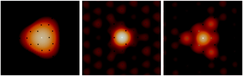 | ||
| Fig. 10 STM simulated images of a single H atom adsorbed on graphene (left) and on the upward and downward displaced Si atoms on silicene (middle and right panels). Dots represent lattice atoms, with grey (black) for the upper (lower) buckled Si atoms. | ||
 | ||
| Fig. 11 STM simulated images of (syn) ortho- and para-hydrogen dimers on silicene (top left and top right, respectively) and of the two possible (syn) meta-dimers, with the adatoms either in the upper-buckled (bottom left) or in the lower-buckled (bottom right) sublattice. Dark dots represent lattice atoms, with grey (black) for the upper (lower) buckled Si atoms, and white dots for the H atoms. | ||
Fig. 10 shows a region containing a single H adatom, either in the upward (i.e. toward the tip) or in the downward displaced Si atom (middle and right panel), and for comparison H on graphene (left panel). In the latter case the “midgap state” is clearly visible in the simulated image, as a bright spot with a characteristic threefold symmetry protruding toward the para positions and decaying slowing away from the defect position. In graphene, these features have been subjected to several experimental investigations and carefully analyzed, e.g., for a carbon atom vacancy.72 Interestingly, simulated images for silicene reveal quite distinctive features associated with the sublattice position of the adsorbed atom, obviously related to the buckling pattern of the silicene sheet. When adsorption occurs on an upper-buckled Si atom the H atom is closer to the tip and determines the bright spot; the π midgap state, localized on the lower-buckled lattice, is hardly visible and its contribution is generally masked by that of the upper-buckled Si atoms. In contrast, when adsorption occurs on a lower-buckled Si atom the π-midgap state localizes on the upper-buckled sublattice and the bright spot closely resembles that found on graphene. These results suggest that if silicene is not strongly interacting with a substrate STM imaging can be used to discriminate the two sublattice position.
Fig. 11 shows the simulated images for a number of compact dimers, the ortho-, meta- and para-dimers discussed in the previous section (all on the same face, for simplicity). Again differently from graphene – where these dimers always generate reflection-symmetric spots around their midpoint – in silicene the presence of a upper-buckled and lower-buckled sublattice manifests itself in the simulated images. This is particularly evident for the (most stable) “balanced” dimers (ortho- and para-dimers) which, occupying both sublattices, display at the same time the two single-H atom features described above, roughly superimposed to each other. This is rather surprising because it suggests that the (balanced) dimers have some open-shell character. In other words, differently to what happens in graphene, in silicene the midgap states induced by two adatoms sitting on opposite sublattices do not “annihilate” completely, rather retain some singly occupied character. This is consistent with the DOSs reported in Fig. 7 which show clearly resolved, though broadened, resonances in the vicinity of the Fermi level, resulting from the incomplete hybridization of the midgap states. On the other hand, the (magnetic) meta-dimers display features which are related to the presence of sharp peaks in the DOS, a pair of midgap states centered around the adatoms and occupying the majority sublattice sites. The latter belong to the lower-buckled sublattice when the meta-dimer is placed on top of upper-buckled Si atoms and on the upper-buckled one in the opposite case. In the first case the midgap states are hardly visible in the STM image, which only show the contribution of the protruding H atoms. In the latter case, on the other hand, they become clearly visible as bright and extended features around the dimer.
4 Summary and concluding remarks
We performed a thorough investigation of the hydrogenation process of free-standing silicene, relevant for the yet to be realized situations where silicene sheets are suspended or placed on an inert substrate, e.g. h-BN. We considered the adsorption of atomic hydrogen starting from the very first adsorption event, and investigated the formation of dimers and of more complex adatom structures on the surface. Similarly to graphene we found that the adsorption of small amounts of H atoms produces local distortions in the lattice and, importantly, introduces “midgap” states which semilocalize around the adatoms and decay slowly away from them. These states are important scattering centers for charge carriers, behave as free local magnetic moments and (thermodynamically) favor secondary adsorption on specific lattice positions. However, we found that H-atom adsorption is always barrierless and thus predict that in silicene, contrary to graphene, dimer formation and clustering is not observable unless thermodynamic conditions prevail during the adsorption process. These findings were rationalized in terms of π bond strength and lattice stiffness: in silicene π bonds are weaker and the lattice is softer than in graphene. As a consequence, similar conclusions on the adsorption process are expected for a large number of simple ad-species which form single covalent bonds with Si lattice sites. Halogenation, for instance, has been considered in the saturation limit, both theoretically26–28 and experimentally,29 as an effective way of tuning the band gap of silicene, by exploiting the influence that the electronegativity of the ad-species has on the energy and the composition of the valence band maxima and conduction band minima. In this context it is worth noticing that in the low density limit considered in this work halogen atoms may behave radically different from each other, and show an ionic rather than a covalent interaction with the Si sheet. In graphene, for instance, only fluorine forms a strong covalent bond with a C atom of the sheet, the other halogens favour ionic binding and induce a mere shift to the Fermi level rather than forming a midgap state.83One important consequence of the above findings is that a smaller mobility of charge carriers has to be expected in silicene when compared to graphene. This is due to the fact the larger amount of resonant scatterers can be gathered by the surface during the fabrication process, i.e. the larger sensitivity of the silicon sheet towards contaminants. In addition, the absence of clustering prevents the conversion of strong, resonant scattering centers (the single adatoms) into more common short-range scatterers (balanced dimers and larger clusters), which are known to have a much smaller effect on mobility, since their contribution to the DC resistivity reads as2,5
Finally, we showed that most of the investigated hydrogenated structures provide clear features when imaged using STM techniques, thereby suggesting a simple method to unambiguously identify these structures in experiments and verify our predictions.
Acknowledgements
This work has been supported by the CINECA High Performance Computing Center through an ISCRA initiative grant (2015).References
- K. S. Novoselov, A. K. Geim, S. V. Morozov, D. Jiang, Y. Zhang, S. V. Dubonos, I. V. Gregorieva and A. A. Firsov, Science, 2004, 306, 666 CrossRef CAS PubMed.
- N. M. R. Peres, Rev. Mod. Phys., 2010, 82, 2673 CrossRef CAS.
- D. S. L. Abergel, V. Apalkov, J. Berashevich, K. Ziegler and T. Chakraborty, Adv. Phys., 2010, 59, 261 CrossRef CAS.
- S. Das Sarma, S. Adam, E. H. Hwang and E. Rossi, Rev. Mod. Phys., 2011, 83, 407–470 CrossRef CAS.
- M. Katsnelson, Graphene: Carbon in Two Dimensions, Cambridge University Press, 2012 Search PubMed.
- D. N. Basov, M. M. Fogler, A. Lanzara, F. Wang and Y. Zhang, Rev. Mod. Phys., 2014, 86, 959–994 CrossRef CAS.
- K. S. Novoselov, D. Jiang, F. Schedin, T. J. Booth, V. V. Khotkevich, S. V. Morozov and A. K. Geim, Proc. Natl. Acad. Sci. U. S. A., 2005, 102, 10451–10453 CrossRef CAS PubMed.
- J. N. Coleman, et al. , Science, 2011, 331, 568–571 CrossRef CAS PubMed.
- P. Vogt, P. De Padova, C. Quaresima, J. Avila, E. Frantzeskakis, M. C. Asensio, A. Resta, B. Ealet and G. Le Lay, Phys. Rev. Lett., 2012, 108, 155501 CrossRef PubMed.
- E. Gibney, Nature, 2015, 572, 274 CrossRef PubMed.
- C. Grazianetti, E. Cinquanta and A. Molle, 2D Mater., 2016, 3, 012001 CrossRef.
- C.-C. Liu, W. Feng and Y. Yao, Phys. Rev. Lett., 2011, 107, 076802 CrossRef PubMed.
- C.-C. Liu, H. Jiang and Y. Yao, Phys. Rev. B: Condens. Matter Mater. Phys., 2011, 84, 195430 CrossRef.
- M. Ezawa, J. Phys. Soc. Jpn., 2015, 84, 121003 CrossRef.
- M. Ezawa, New J. Phys., 2012, 14, 033003 CrossRef.
- M. Ezawa, Appl. Phys. Lett., 2013, 102, 172103 CrossRef.
- M. Noor-A-Alam, H. J. Kim and Y.-H. Shin, J. Appl. Phys., 2015, 117, 224304 CrossRef.
- A. H. Castro Neto and F. Guinea, Phys. Rev. Lett., 2009, 103, 026804 CrossRef CAS PubMed.
- J. Zhou, Q. Liang and J. Dong, Carbon, 2010, 48, 1405–1409 CrossRef CAS.
- J. Balakrishnan, G. K. W. Koon, M. Jaiswal, A. H. C. Neto and B. Ozyilmaz, Nat. Phys., 2013, 9, 284–287 CrossRef CAS.
- L. Tao, E. Cinquanta, D. Chiappe, C. Grazianetti, A. Fanciulli, M. Dubey, A. Molle and D. Akinwande, Nat. Nanotechnol., 2015, 10, 227–231 CrossRef CAS PubMed.
- T. H. Osborn, A. A. Farajian, O. V. Pupysheva, R. S. Aga and L. L. Y. Voon, Chem. Phys. Lett., 2011, 511, 101–105 CrossRef CAS.
- M. Houssa, E. Scalise, K. Sankaran, G. Pourtois, V. V. Afanasev and A. Stesmans, Appl. Phys. Lett., 2011, 98, 223107 CrossRef.
- C. Wen Zhang and S. Shen Yan, J. Phys. Chem. C, 2012, 116, 4163–4166 Search PubMed.
- B. Huang, H.-X. Deng, H. Lee, M. Yoon, B. G. Sumpter, F. Liu, S. C. Smith and S.-H. Wei, Phys. Rev. X, 2014, 4, 021029 Search PubMed.
- N. Gao, W. T. Zheng and Q. Jiang, Phys. Chem. Chem. Phys., 2012, 14, 257–261 RSC.
- B. Huang, H. J. Xiang and S.-H. Wei, Phys. Rev. Lett., 2013, 111, 145502 CrossRef PubMed.
- Q. G. Jiang, J. F. Zhang, Z. M. Ao and Y. P. Wu, Sci. Rep., 2015, 5, 3954 Search PubMed.
- W. Li, S. Sheng, J. Chen, P. Cheng, L. Chen and K. Wu, Phys. Rev. B: Condens. Matter Mater. Phys., 2016, 93, 155410 CrossRef.
- Y. Du, J. Zhuang, H. Liu, X. Xu, S. Eilers, K. Wu, P. Cheng, J. Zhao, X. Pi, K. W. See, G. Peleckis, X. Wang and S. X. Dou, ACS Nano, 2014, 8, 10019–10025 CrossRef CAS PubMed.
- J. Qiu, H. Fu, Y. Xu, Q. Zhou, S. Meng, H. Li, L. Chen and K. Wu, ACS Nano, 2015, 9, 11192–11199 CrossRef CAS PubMed.
- J. Qiu, H. Fu, Y. Xu, A. I. Oreshkin, T. Shao, H. Li, S. Meng, L. Chen and K. Wu, Phys. Rev. Lett., 2015, 114, 126101 CrossRef PubMed.
- R. Martinazzo, S. Casolo and G. F. Tantardini, in Physics and Application of Graphene – Theory, ed. S. Mikhailov, InTech, Rijeka, Croatia, 2011, p. 45 Search PubMed.
- R. Martinazzo, S. Casolo and L. Hornekær, in Dynamics of Gas-Surface Interactions - Atomic-level Understanding of Scattering Processes at Surfaces, ed. R. Diez-Muiño and F. H. Busnengo, Springer series in Surface Science, Springer, Berlin, 2013, p. 157 Search PubMed.
- R. Martinazzo, in Graphene Science Handbook, ed. M. Aliofkhazraei, N. Ali, W. I. Milne, C. S. Ozkan, S. Mitura and J. L. Gervasoni, CRC Press, 2016, in press Search PubMed.
- F.-B. Zheng and C.-W. Zhang, Nanoscale Res. Lett., 2012, 7, 1–5 CrossRef PubMed.
- P. Zhang, X. Li, C. Hu, S. Wu and Z. Zhu, Phys. Lett. A, 2012, 376, 1230–1233 CrossRef CAS.
- S. Trivedi, A. Srivastava and R. Kurchania, J. Comput. Theor. Nanosci., 2014, 11, 781–788 CrossRef CAS.
- B. van den Broek, M. Houssa, E. Scalise, G. Pourtois, V. Afanasev and A. Stesmans, Appl. Surf. Sci., 2014, 291, 104–108 CrossRef CAS.
- S.-Y. Lin, S.-L. Chang, N. T. Thuy Tran, P.-H. Yang and M.-F. Lin, Phys. Chem. Chem. Phys., 2015, 17, 26443–26450 RSC.
- W. C. Wu, Z. M. Ao, C. H. Yang, S. Li, G. X. Wang, C. M. Li and S. Li, J. Mater. Chem. C, 2015, 3, 2593–2602 RSC.
- C. J. Rupp, S. Chakraborty, R. Ahuja and R. J. Baierle, Phys. Chem. Chem. Phys., 2015, 17, 22210–22216 RSC.
- Q. G. Jiang, J. F. Zhang, Z. M. Ao and Y. P. Wu, J. Mater. Chem. C, 2015, 3, 3954–3959 RSC.
- J. M. Soler, E. Artacho, J. D. Gale, A. García, J. Junquera, P. Ordejón and D. Sánchez-Portal, J. Phys.: Condens. Matter, 2002, 14, 2745 CrossRef CAS.
- J. P. Perdew, K. Burke and M. Ernzerhof, Phys. Rev. Lett., 1996, 77, 3865 CrossRef CAS PubMed.
- J. P. Perdew, K. Burke and M. Ernzerhof, Phys. Rev. Lett., 1997, 78, 1396 CrossRef CAS.
- N. Troullier and J. L. Martins, Phys. Rev. B: Condens. Matter Mater. Phys., 1991, 43, 1993–2006 CrossRef CAS.
- S. G. Louie, S. Froyen and M. L. Cohen, Phys. Rev. B: Condens. Matter Mater. Phys., 1982, 26, 1738–1742 CrossRef CAS.
- H. J. Monkhorst and J. D. Pack, Phys. Rev. B: Condens. Matter Mater. Phys., 1976, 13, 5188–5192 CrossRef.
- S. Cahangirov, M. Topsakal, E. Aktürk, H. ahin and S. Ciraci, Phys. Rev. Lett., 2009, 102, 236804 CrossRef CAS PubMed.
- E. Cinquanta, E. Scalise, D. Chiappe, C. Grazianetti, B. van den Broek, M. Houssa, M. Fanciulli and A. Molle, J. Phys. Chem. C, 2013, 117, 16719–16724 CAS.
- P. De Padova, C. Quaresima, B. Olivieri, P. Perfetti and G. Le Lay, Appl. Phys. Lett., 2011, 98, 081909 CrossRef.
- E. F. Sheka, Int. J. Quantum Chem., 2013, 113, 612–618 CrossRef CAS.
- X. Sha and B. Jackson, Surf. Sci., 2002, 496, 318–330 CrossRef CAS.
- M. Zhang, Y. Kan, Q. Zang, Z. Su and R. Wang, Chem. Phys. Lett., 2003, 379, 81–86 CrossRef CAS.
- R. Zhang, S. Lee, C.-K. Law, W.-K. Li and B. K. Teo, Chem. Phys. Lett., 2002, 364, 251–258 CrossRef CAS.
- A. Kramida, Yu. Ralchenko, J. Reader and NIST ASD Team, NIST Atomic Spectra Database (ver., 5.1), [Online]. Available: http://physics.nist.gov/asd [2014, March 31]. National Institute of Standards and Technology, Gaithersburg, MD., 2013.
- M. Mohr, J. Maultzsch, E. Dobardžić, S. Reich, I. Milošević, M. Damnjanović, A. Bosak, M. Krisch and C. Thomsen, Phys. Rev. B: Condens. Matter Mater. Phys., 2007, 76, 035439 CrossRef.
- N. J. Roome and J. D. Carey, ACS Appl. Mater. Interfaces, 2014, 6, 7743–7750 CAS.
- S. Casolo, O. M. Løvvik, R. Martinazzo and G. F. J. Tantardini, Chem. Phys., 2009, 130, 054704 Search PubMed.
- S. Boys and F. Bernardi, Mol. Phys., 1970, 19, 553–566 CrossRef CAS.
- A. A. Dzhurakhalov and F. M. Peeters, Carbon, 2011, 49, 3258–3266 CrossRef CAS.
- M. Bonfanti, S. Casolo, G. Tantardini, A. Ponti and R. Martinazzo, J. Chem. Phys., 2011, 135, 164701 CrossRef CAS PubMed.
- V. O. Ozcelik and S. Ciraci, J. Phys. Chem. C, 2013, 117, 26305–26315 CAS.
- T. H. Osborn, A. A. Farajian, O. V. Pupysheva, R. S. Aga and L. L. Y. Voon, Chem. Phys. Lett., 2011, 511, 101–105 CrossRef CAS.
- Q. G. Jiang, J. F. Zhang, Z. M. Ao and Y. P. Wu, J. Mater. Chem. C, 2015, 3, 3954–3959 RSC.
- J. V. Barth, Surf. Sci. Rep., 2000, 40, 75–149 CrossRef CAS.
- L. Hornekær, E. Rauls, W. Xu, Ž. Šljivančanin, R. Otero, I. Stensgaard, E. Læegsgaard, B. Hammer and F. Besenbacher, Phys. Rev. Lett., 2006, 97, 186102 CrossRef PubMed.
- T. O. Wehling, M. I. Katsnelson and A. I. Lichtenstein, Phys. Rev. B: Condens. Matter Mater. Phys., 2009, 80, 085428 CrossRef.
- V. M. Pereira, F. Guinea, J. Lopes dos Santos, N. Peres and A. Castro Neto, Phys. Rev. Lett., 2006, 96, 036801 CrossRef PubMed.
- V. M. Pereira, J. M. B. Lopes dos Santos and A. H. Castro Neto, Phys. Rev. B: Condens. Matter Mater. Phys., 2008, 77, 115109 CrossRef.
- M. M. Ugeda, I. Brihuega, F. Guinea and J. M. Gomez-Rodriguez, Phys. Rev. Lett., 2010, 104, 096804 CrossRef CAS PubMed.
- P. Haase, S. Fuchs, T. Pruschke, H. Ochoa and F. Guinea, Phys. Rev. B: Condens. Matter Mater. Phys., 2011, 83, 241408(R) CrossRef.
- E. H. Lieb, Phys. Rev. Lett., 1989, 62, 1201–1204 CrossRef PubMed.
- M. Casartelli, S. Casolo, G. F. Tantardini and R. Martinazzo, Phys. Rev. B: Condens. Matter Mater. Phys., 2013, 88, 195424 CrossRef.
- M. Casartelli, S. Casolo, G. F. Tantardini and R. Martinazzo, Carbon, 2014, 77, 165–174 CrossRef CAS.
- Z.-G. Shao, X.-S. Ye, L. Yang and C.-L. Wang, J. Appl. Phys., 2013, 114, 093712 CrossRef.
- K. I. Bolotin, K. J. Sikes, J. Hone, H. L. Stormer and P. Kim, Phys. Rev. Lett., 2008, 101, 096802 CrossRef CAS PubMed.
- K. Bolotin, K. Sikes, Z. Jiang, M. Klima, G. Fudenberg, J. Hone, P. Kim and H. L. Stormer, Solid State Commun., 2008, 143, 351 CrossRef.
- W. C. Wu, Z. M. Ao, C. H. Yang, S. Li, G. X. Wang, C. M. Li and S. Li, J. Mater. Chem. C, 2015, 3, 2593–2602 RSC.
- W. Wu, Z. Ao, T. Wang, C. Li and S. Li, Phys. Chem. Chem. Phys., 2014, 16, 16588 RSC.
- M. J. Frisch, et al., Gaussian 03, Revision C., 02, Gaussian Inc., Wallingford, CT, 2004 Search PubMed.
- M. Klintenberg, S. Lebègue, M. I. Katsnelson and O. Eriksson, Phys. Rev. B: Condens. Matter Mater. Phys., 2010, 81, 085433 CrossRef.
Footnotes |
| † Present address: Institute of Physics, Ecole Polytechnique Fédérale de Lausanne (EPFL), CH-1015 Lausanne, Switzerland. |
| ‡ The overlayers are referenced to the metal substrate, i.e. 4 × 4 is 3 × 3 if referenced to free-standing silicene. |
| § There is some uncertainty in this value. Commonly used values are 10.6 eV and 5.6 eV for C and Si, respectively, following the semiempirical PM3 calculations of ref. 56. LDA density-functional theory calculations give 8.21 eV and 6.66 eV, respectively, whereas literature spectroscopic data result in 7.95 eV and 5.62 eV (excitation energies to the lowest-lying triplet states 3DJ[nsnp3], averaged over the J terms. Data from ref. 57). |
| ¶ Lieb's result states that, at half-filling, the spin S of the ground-state matches the sublattice imbalance, S = ℏ|nA − nB|/2, where nA(nB) is the number of sites in the A(B) sublattice. |
| || This finding does not contradict Lieb's result above. The (midgap) impurity-induced band remains flat – and the system magnetic – as long as the substrate is bipartite (electron–hole symmetric). In realistic cases, though, the introduction of any kind of defect breaks the e–h symmetry in a substantial way, by modifying the on-site energies of the sites closest to the defects, as it was shown in the case of a carbon atom vacancy in graphene.75,76 Hence, Lieb's theorem does not rigorously hold in these situations. |
| ** The room-temperature intrinsic mobility was computed with first-principles means and found to be ∼3.3(3.3) × 105 cm2 V−1 s−1 for electrons (holes) in graphene and ∼2.6(2.2) × 105 cm2 V−1 s−1 in silicene.77 |
| †† If the above mentioned intrinsic mobilities are taken into account using Matthiessen's rule this estimate changes to nimp ∼ 4 × 10⁻⁶ for graphene and remains unchanged for silicene. |
| This journal is © the Owner Societies 2016 |