 Open Access Article
Competitive effects of oxygen vacancy formation and interfacial oxidation on an ultra-thin HfO2-based resistive switching memory: beyond filament and charge hopping models†
Hisao
Nakamura
*ab and
Yoshihiro
Asai
b
aResearch Planning Office, Department of Materials and Chemistry, National Institute of Advanced Industrial Science and Technology (AIST), 1-1-1 Umezono, Tsukuba Central 1, Tsukuba, Ibaraki 305-8560, Japan. E-mail: hs-namaura@aist.go.jp
bResearch Center for Computational Design of Advanced Materials, National Institute of Advanced Industrial Science and Technology (AIST), 1-1-1 Umezono, Tsukuba Central 2, Tsukuba, Ibaraki 305-8568, Japan
First published on 2nd March 2016
Abstract
We studied the quantum transport mechanism of an ultra-thin HfO2-based resistive random access memory (ReRAM) cell with TiN electrodes and proposed the design of a sub-10 nm scale device. It is believed that formation and rupture of the conduction path in the local filament causes the switching between high and low resistive states. However, the validity of this simple filament model is not obvious in the sub-10 nm scale device because the redox processes occur mainly in a few nm range at the interface. Furthermore, the intrinsic transport mechanism of the device, in particular, quantum coherence, depends on device materials and length-scale. The relationship between the redox states and the transport mechanism like ballistic or hopping is still under debate when the device length scale is less than 10 nm. In the present study, we performed first-principles calculations of the non-equilibrium Green's function including electron–phonon interactions. We examined several characteristic structures of the HfOx wire (nano-scale conduction path) and the interfaces between the resistive switching layer and electrodes. We found that the metal buffer layer induced a change in the oxygen-reduction site from the interface of HfOx/TiN to the buffer layer. Even when the inserted buffer layer is a few atomic layers, this effect plays an important role in the enhancement of the performance of ON/OFF resistive switching and in the reduction of the inelastic electric current by electron–phonon scattering. The latter suppresses the hopping mechanism, which makes the ballistic conduction the dominant mechanism. We evaluated the activation energy in the high temperature limit by using the first-principles results of inelastic current. Our theoretical model explains the observed crossover of the temperature dependence of ReRAM cells and gives a new insight into the principle of operation on a sub-10 nm scale ReRAM device.
Introduction
Nonvolatile memory has become one of the major research targets in nanoelectronics because of society's need for low power devices, big data technology, and data-driven information processes. Resistive random access memory (ReRAM) is one of the most promising next-generation nonvolatile memory technologies and has been attracting increasing attention because of its capability for high-density integration as well as its fast and low power operation. However, the problematic issue of large variation in resistance values must still be resolved to enable the practical use of this technology.1 The fundamental structure of the ReRAM cell is simple. The cell consists of two electrodes and a resistive switching layer (RSL) usually made of a transition metal oxide that is placed between the two electrodes. The filament model has been frequently used for the discussion of the ReRAM operation mechanism. The mechanism consists of two steps: (a) first, the filament is formed in the RSL during the fabrication process and (b) the filament is connected/disconnected to/from the electrode by oxygen (Ox) migration [oxygen vacancies (Vo)]2–4 in the ON/OFF switching operation that is sometimes called the SET/RESET process. This either creates or annihilates the current path. The thickness of the memory cell and the RSL has continuously decreased and is now below 10 nm and 5 nm, respectively, in order to enable low voltage read/write operation below 0.2 V.5,6 While the switching of ReRAM is either unipolar or bipolar and usually depends on the RSL material, switching is exclusively bipolar when the thickness decreases well below 10 nm.7 In such an ultra-thin RSL, the concept of the filament becomes ill-defined and Vo migration predominantly occurs at the interface rather than in the filament. Thus, the filament model should be replaced by the unified redox model, where resistive switching occurs as the result of a redox reaction at the interface between the Ox donor (RSL) and the acceptor (electrode).8 The unified redox model implicitly involves Schottky barrier modulation due to oxidation.While the overall switching mechanism has been elucidated as described above, a microscopic description of the switching mechanism and the redox processes still remains an open question. Unfortunately, the roles of Vo distribution in the RSL and the oxidized interface for the ReRAM cell performance have been largely unexplored. Because of this, the electric transport and the switching mechanism connecting the high and low resistance states (HRS/LRS) remain a matter of strong debate. While some thermodynamic or kinetic models for the interfacial oxide free energy exist,9,10 these are not very useful for the atomistic understanding and prediction of the current–voltage (I–V) characteristics. It should be stressed that the thickness of the RSL in the ReRAM cell has been reduced to the length scale around 10 nm, which is already well within the length regime where the quantum transport theory becomes necessary. Despite its rather phenomenological nature, the quantum point contact theory was tested in comparison with the observed I–V characteristics of the LRS.11–13 However, the application of a high-quality quantum transport theory is necessary to obtain the microscopic understanding of the I–V characteristics of the ReRAM cell.
In the present study, we use the first-principles quantum transport simulation method to study the I–V characteristics of the ultra-thin HfO2-based ReRAM cells. Because of their ease of fabrication, TiN electrodes are frequently used in experiments and were therefore used in our calculations as well. We focus on the studies of LRS and HRS in the low bias regime (typically up to 0.2 V) using the non-equilibrium Green's function theory calculations based on the density functional approximation (NEGF-DFT).14 The impact of interfacial oxidation on the electric current ON/OFF ratio and the transport mechanism is discussed in terms of NEGF-DFT augmented by the electron–phonon coupling correction.
Computational model for the ultra-thin ReRAM cell
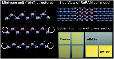
We introduce a structure model defined by the minimal unit cell consisting of a single HfO2 wire, which relates to c-HfO2 phase, and two (1 × 1) cubic TiN electrodes with the (001) interface. We call this minimal unit cell a “bin”. To make the unit cell of a heterojunction consisting of HfO2 and TiN, strain is imposed on each lattice constant. Within the present DFT calculations, the strain of a and b axes is 3% for HfO2 and 13% for TiN, respectively. The strain of the c-axis imposed on TiN is 6% while that of HfO2 is almost negligible. We note that the effect of the resulting strain of TiN electrodes is not important for the present purpose, i.e., analysis of transport properties of HRS and LRS.15 The HfO2 part of the bin involves nine Hf layers corresponding to the thickness of around 2.2 nm. To model the electrodes, we include 14 layers of TiN for each of the two sides; thus, the total thickness of the cell is approximately 8.0 nm. Our device model for the TiN/HfOx/TiN cell consists of four bins, i.e., we use a supercell containing a bundle of 2 × 2 bins, as shown in Fig. 1. We investigate several possibilities for LRS of the ReRAM cell by removing some O atoms from the four bins. A single bin has three possible states, i.e., “off” (no Vo), “4Vo” (formation of four Vo), and “8Vo” (formation of eight Vo), as shown in Fig. 1. We examine two possible LRS structures out of all possible states that can be obtained by combinations of the three possibilities of the single bin in the cell. One possible structure consists of four 4Vo-bins, and we call this the L1 cell model. The other structure has two 8Vo-bins and two off-bins; we call this the L2 cell model. In other words, L1 consists of four Ox-reduced HfO1.33 nanowires, and L2 has two HfO0.89 metallic nanowires. For HRS, a cell consisting of four off-bins is considered and is called the H1 cell model. It is very important to keep the removed O atoms at the interface between HfO2 and TiN electrodes, as shown in Fig. 1. This ensures that the model structure conserves the number of total atoms. This structural model explicitly takes into account the effect of the interfacial oxidation caused by Ox migration on the first-principles NEGF-DFT transport calculations.To ensure that the bin model provides a reasonable structural model for the cell, we perform full optimization of the atomic geometry of the cell. The calculation results are summarized in Table S1 of the ESI,† and it can be seen that the bin model performs fairly well for the case of the Ox-reduced HfO1.33 nanowire L1 model. We also examine the L2 cell model that includes the HfO0.89 metallic wire. Here as well, the introduced geometry is stable against the optimization, demonstrating the validity of the bin model. We then use the present cell to evaluate the enthalpy difference between the two redox states given by 4Vo-bin → 8Vo-bin + oxidized. The calculated value is −0.54 eV, i.e., the relative stabilities of the two states are comparable and the reaction can be energetically reversible. Thus, the bin model provides a reasonable structural model that enables the study of the transport mechanism of the ReRAM cell using NEGF-DFT calculations.
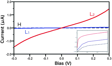
The first-principles results of the I–V curve for the H1, L1, and L2 cell models are summarized in Fig. 2. No differences between the electric current for one of the possible LRS and HRS represented by the L1 cell model and the H1 cell model can be seen in the figure, and the currents for the H1 and the L1 cell models are both small. In the previous study, we obtained a similar result for the comparison between the off-bins and the 4Vo single bins.16 The observed similar results are reasonable because the atomic structure in the H1 (L1) cell model is close to a simple 2 × 2 multiplication of the single bin systems. On the other hand, the obtained electric current for the L2 cell model is more than 10 times larger than that for the L1 cell model, although the total amount of O deficiency within the cell is the same in these two cases. The results indicate that a local Vo accumulation is necessary to obtain a larger ON/OFF ratio. This may mean that a thicker (Vo-rich) conduction path (filament) is required. However, in both cases, the transmission probability around the Fermi energy EF (we set EF = 0.0 eV), i.e., [−0.3 eV, 0.3 eV], is still small, below 0.1; thus, LRS is at best a poor metallic state. Because the band gap of the bulk HfO1.33 is close to zero, our result may imply the formation of a barrier at the interface between the RSL and the electrode because of the oxidized interface originating from the migration of Ox. In the next section, we discuss this quantum point contact effect qualitatively.
Multi-layer ReRAM cell and point contact modulation by the oxidized interface
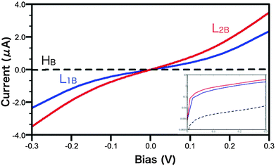
The insertion of a metal buffer layer can significantly affect the ReRAM cell properties. The metallic interlayer is usually used as an Ox scavenger and/or an acceptor in the SET process for the ReRAM cell,17 and an insertion of the metal buffer layer may increase the Ox content in the RSL. Interfacial barrier reduction is another possible benefit of metal buffer layer insertion. The buffer layer insertion may protect the TiN electrode interface from the barrier formation because the barrier height formed at the metal buffer layer may be smaller than the barrier height formed at the TiN electrode interface. Both these possibilities can have a strong impact on the I–V characteristics of the ReRAM cell. We therefore investigate these effects using first-principles calculations by including the atomic buffer layer in our cell model. The metal buffer layer is denoted as MB. A single atomic monolayer of tantalum is inserted at the interface between the RSL and the electrode. The monolayer insertion is made for both terminal interfaces of the RSL with the two electrodes. The resulting cell models are denoted as H1B, L1B, and L2B, corresponding to their original H1, L1, or L2 cells. The bin model and the construction method are then used to build the model structures for the monolayer-inserted cell.We performed first-principles relaxation of atomic coordinates to determine the atomic geometries for the three bin states with the obtained structural parameters summarized in Table S1 of ESI.† The I–V curves for the cell models L1B and L2B are shown in Fig. 3. While the electric current for the H1B cell model is quite small within the bias voltage range, similar to the case for the H1 cell model, because of the MB insertion, the electric current for the cell model L1B is much larger than that for the L1 cell. Because the Vo concentration and arrangement in the bins are fairly similar for the L1 and L1B cell models, this result suggests that the oxidized MBOx/TiN (L1B) interface reduces the barrier height of the Ox-TiN/TiN (L1) system, where Ox-TiN denotes the interfacial oxygen and the most outer TiN layer, i.e., oxidized TiN surface. Our first-principles results support the hypothesis of barrier height reduction by buffer layer insertion. We also find that buffer layer insertion enhances the electric current in the case of the cell model L2B, further supporting this hypothesis. The electronic coupling strength between the oxidized interface and the bulk electrode is estimated from the imaginary part of the complex eigenvalue of the effective molecular projected state Hamiltonian (MPSH).18 The calculated values close to EF are approximately 0.07 eV and 1.15 eV for Ox-TiN and MBOx, respectively, indicating that the contact resistance is smaller for the L1B cell than for the L1 cell. This directly demonstrates that the barrier height is reduced by buffer layer insertion. Both the barrier height and the filament thickness play important roles in controlling the I–V characteristics of the ReRAM cell. Therefore, the reduction of the barrier height in metal buffer layer cells found by our calculations can explain the experimentally observed improvement of the current ON/OFF ratio of the TiN/HfOx/TiN cell upon insertion of the 5 nm-thick Hf buffer layer.17,19 While there is a difference in the thicknesses of the buffer layers in our calculation and in the experiment, the physics underlying the effect of buffer layer insertion is common to both cases.
Electron–phonon interactions and temperature dependence
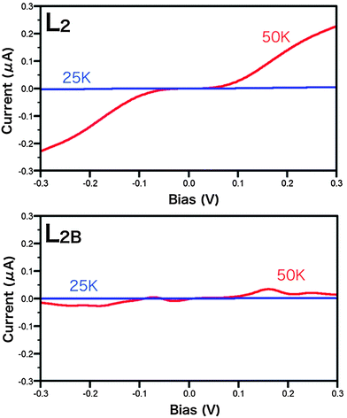
Experimentally, activation-type temperature dependence of the conductance has been observed for the ReRAM cell, suggesting a hopping conduction mechanism.19,20 While this may cast some doubt on the applicability of the quantum transport theory,21,22 buffer layer insertion dramatically reduces the temperature dependence; therefore, no temperature dependence is experimentally observed in this case.17 This strongly suggests that the ballistic mechanism dominates the conduction. Below the thickness of 10 nm, the activation energy for the HfO2-based ReRAM cell becomes as small as 0.05–0.10 eV,17,19,20 enabling the description of the conduction with the quantum transport theory. To uncover the physics underlying these findings, it is necessary to use a theory that describes both the hopping and the ballistic transport mechanisms. Here we adopt the perturbation approach for the electron–phonon coupling effect. The most elaborate self-consistent theory for the electric and phonon currents including the electron–phonon coupling effects between them23 describes the activation-type temperature dependence. We derived a scaling function from the calculation result obtained by using the self-consistent theory and a model Hamiltonian and found that it describes the experimental temperature dependence in the hopping regime.24 The perturbation approach followed by the scaling function analysis is useful for the present study; however, here we adopt the first-principles lowest order expansion (LOE) theory, neglecting the phonon current, which is a reasonable choice for realistic computational resources.14,25The plots of electric current versus bias voltage that include the electron–phonon coupling effect for the L2 and L2B cell models are shown in Fig. 4. To discuss the temperature (T) dependence, we use the plots at T = 25 K and at T = 50 K. Distinct temperature dependence is obtained for the two models. While the current increases with increasing temperature in the case of the L2 model, no clear increase can be observed for the L2B model. Fig. 5 shows the temperature dependent resistance R defined in terms of the inverse of the differential conductance at V = 0.1, i.e.,  . In this plot, the resistance is scaled by the resistance at T = 0 K. The resistance for the L2 model decreases rather steeply with increasing temperature; therefore, as the temperature is increased from 50 K to 200 K, the resistance is reduced to approximately 20% of its original value. On the other hand, the temperature dependence for the L2B model is much weaker, suggesting a larger role of the ballistic mechanisms for the conduction. Thus, the insertion of the buffer layer changes the conduction mechanism from hopping (L2) to quasi-ballistic (L2B).
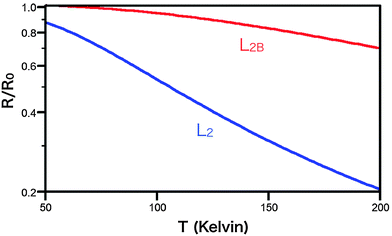 | ||
| Fig. 5 The plot of the resistance of LRS (L2 and L2B) as a function of temperature. Each resistance value is normalized by that of the zero temperature limit. | ||
We now discuss the reason for the reduction of the temperature dependence by buffer layer insertion. Within a simple single level model, the resistance ratio R/R0 is given as follows:26
 | (1) |
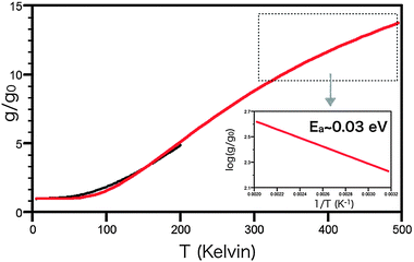
To further check the validity of our modeling, we also estimate the activation energy Ea according to Marcus theory for the scenario of charge trap (i.e., carrier localization) at the Vo site, which has often been adopted for ReRAM device simulation. We derive the Marcus parabola of the donor–acceptor states by injecting an electron charge into the Vo site. According to the theoretical study of polaron self-trapping at HfO2 defects, Vo2− is thermodynamically more stable than Vo−.30 We calculate the potential profile and estimate the activation energy. The obtained values for the Vo2− state are 2.6 eV and 0.6 eV for the non-adiabatic limit and the adiabatic limit of charge transfer, respectively. These estimates are much higher than the experimentally estimated value. Even when the trapping state is assumed to be Vo−, the activation energy values are 1.1 eV (non-adiabatic limit) and 0.4 eV (adiabatic limit), much further from the experimental result than the estimate obtained from Fig. 6.
We conclude that the NEGF-DFT method with the electron–phonon coupling correction is reasonably accurate for the study of the ReRAM cell below 10 nm thickness. We emphasize that the main difference between the electronic structures of the L2 and L2B models is the electronic coupling strength of the conduction state in the RSL with Ox-TiN and MBOx interfaces. The present results indicate that the change in the conduction mechanism from hopping to ballistic conduction caused by buffer layer insertion is explained within our theory.
Summary
Here we study the I–V characteristics of ultra-thin HfO2-based ReRAM cells in the low-bias voltage regime using the quantum transport theory amended by the lowest order electron–phonon coupling correction. We describe the justification for this approach and examine several cell models focusing on the role of the oxygen vacancy (Vo) and the metal buffer layer insertion effect. The I–V calculations indicate that the local accumulation of Vo is crucial for the distinct energetically stable ON state. The electronic state of the oxidized contact by the SET process has a strong influence on the transport. The multi-layer cell structure obtained using metal buffer layer insertion is a promising approach to control the redox state at the interface accompanying the SET/REST operation. Our first-principles simulation predicts that the hybridization of conducting wavefunctions at the oxidized interface is crucial for obtaining distinct ON/OFF I–V behavior. We include the electron–phonon interaction effect into the non-equilibrium Green's function theory on the basis of density functional approximation and use it to study the temperature dependence of the resistance of the two low resistance states (LRS). Our results indicate that the electron–phonon coupling effect on the resistance is controlled by buffer layer insertion, with the conduction mechanism changing because of the insertion of the buffer layer. Thus, our study provides guidance for the design of the low-power operation of the ReRAM cell.Method
All DFT calculations were performed using the SIESTA package,31 and the NEGF-DFT transport calculations were then performed using the HiRUNE subroutines developed in-house and interfaced with the SIESTA package.14 We used the local density approximation (LDA) for the exchange–correlation (XC) functional and adopted the single zeta plus polarization function (SZP) level basis set for all atoms. We used 8 × 8 Monkhorst–Pack k-point sampling parallel to the surface direction. Full optimization of the atomic geometry in the cell was applied to the introduced bin models, and the result was compared with the structure obtained from the construction using the local structures of the four bins, i.e., we compared the structures obtained with and without the construction. First, the distance between the two electrodes (Lgap) and the a and b lattice constants are optimized using the first-principles calculations, while the structure of each bin is fixed at the initial geometry. The lattice mismatch between the RSL and the electrode is taken into account within the optimization. Following this, the atomic geometries in the cells are determined by the calculation as all the atoms in the RSL and the two TiN layers closest to the surface are relaxed and optimized. We define the RSL thickness (LRSL) as the distance between the two terminal Hf layers. The difference Lgap − LRSL corresponds to the thickness of the oxidized interface. All structural parameters are listed in the ESI.† To estimate the electronic coupling strength of the conducting RSL states and electrodes, we calculate the effective Hamiltonian using the NEGF-DFT results (see ESI†). The target state to evaluate the electronic coupling strength to the electrode is set to the interface, i.e., TiNO2 and Ta2O2 for with and without the Ta atomic layer, respectively. We evaluate the imaginary part of the elements of the last two terms in eqn (S2) (ESI†) to analyze the electronic coupling strength at the contact.The electron–phonon coupling Mα is evaluated for each selected mode qα by the numerical derivative as ∂H/∂qα, where we consider only the Γ point for the phonon. We calculate the normal modes using the frozen phonon approximation and then select the localized modes in the RSL to evaluate electron–phonon couplings. The electric current is calculated using the NEGF framework with LOE, where 38 and 28 normal modes are explicitly included for L2 and L2B, respectively. For practical calculations of inelastic current using full NEGF-DFT, we adopt the lowest order expansion of Born approximation, which allows the same k-point sampling as that of ballistic transport calculations and the beyond-wideband-limit approximation, while avoiding computational difficulties. The detailed formalism is given in the ESI.†
The activation energy of the charge trap model was evaluated by the following a simplified constrained DFT procedure.32 First, we consider two neighboring Vo sites in the RSL. To inject the trapped electron, we place a pseudo hydrogen (or helium) atom [i.e., a pseudo ion + one/two electron(s)] at the position of one of the Vo and calculate the electron density matrix using the standard DFT technique. The resulting density matrix has the desired excess electron, i.e., Vo− or Vo2− state in comparison with the original RSL. We calculate the Mulliken charge using the atomic orbital basis related to the pseudo atom and find that its value is −1.2 for Vo− and −2.0 for Vo2−. We fix the obtained density matrix and then recalculate the total energy of the original RSL using the same basis set, i.e., the system consists of a RSL with an excess electron on the Vo site. We introduce a background positive charge to simulate the charge-doped RSL and perform the described procedure along the path of the Vo hopping sites. The resulting potential profile gives us the activation energy and the Marcus parabola.
Acknowledgements
H. N. and Y. A. acknowledge discussions and conversations with T. Miayzaki, H. Shima, and H. Akinaga. This work was supported by KAKENHI, a Grant-in-Aid for Scientific Research on Innovation Areas “Molecular Architectonics: Orchestration of Single Molecules for Novel Function” (#2511008). HN thanks the support of the Visiting Professorship Program at Institute for Catalysis, Hokkaido University.References
- H. Akinaga, Recent Advances and Future Prospects in Functional-Oxide Nanoelectronics: The Emerging Materials and Novel Functionalities that are Accelerating Semiconductor Device Research and Development. This is a translated version of the original paper which appeared in Oyo Buturi 81 (2012) 980 [in Japanese], 1–13, Doi: 10.7567/JJAP.52.100001 (2013).
- D. H. Kwon, et al., Atomic structure of conducting nanofilaments in TiO2 resistive switching memory, Nat. Nanotechnol., 2010, 5, 148–153, DOI:10.1038/Nnano.2009.456.
- B. Magyari-Kope, M. Tendulkar, S. G. Park, H. D. Lee and Y. Nishi, Resistive switching mechanisms in random access memory devices incorporating transition metal oxides: TiO2, NiO and Pr0.7Ca0.3MnO3, Nanotechnology, 2011, 22, 254029, DOI:10.1088/0957-4484/22/25/254029.
- M. J. Lee, et al., Electrical Manipulation of Nanofilaments in Transition-Metal Oxides for Resistance-Based Memory, Nano Lett., 2009, 9, 1476–1481, DOI:10.1021/Nl803387q.
- T. H. Hou, et al., Evolution of RESET current and filament morphology in low-power HfO2 unipolar resistive switching memory, Appl. Phys. Lett., 2011, 98, 103511, DOI:10.1063/1.3565239.
- A. Prakash, D. Jana and S. Maikap, TaO (x)-based resistive switching memories: prospective and challenges, Nanoscale Res. Lett., 2013, 8, 418, DOI:10.1186/1556-276x-8-418.
- T. Yanagida, et al., Scaling Effect on Unipolar and Bipolar Resistive Switching of Metal Oxides, Sci. Rep., 2013, 3, 1657, DOI:10.1038/srep01657.
- H. Shima, H. Akinaga, Resistive Random Access Memory (ReRAM) Based on Metal Oxides, Special Issue of IEEE Proceedings “Nanoelectronics Research for Beyond CMOS Information Processing,” 2010, 98, 2237–2251.
- C. B. Lee, et al., Effects of metal electrodes on the resistive memory switching property of NiO thin films, Appl. Phys. Lett., 2008, 93, 042115, DOI:10.1063/1.2967194.
- A. Makarov, V. Sverdlov and S. Selberherr, Stochastic model of the resistive switching mechanism in bipolar resistive random access memory: Monte Carlo simulations, J. Vac. Sci. Technol., B: Nanotechnol. Microelectron.: Mater., Process., Meas., Phenom., 2011, 29, 01ad03, DOI:10.1116/1.3521503.
- E. Miranda, A. Mehonic, J. Suñé and A. J. Kenyon, Multi-channel conduction in redox-based resistive switch modelled using quantum point contact theory, Appl. Phys. Lett., 2013, 103, 222904, DOI:10.1063/1.4836935.
- L. M. Prócel, et al., Experimental evidence of the quantum point contact theory in the conduction mechanism of bipolar HfO2-based resistive random access memories, J. Appl. Phys., 2013, 114, 074509, DOI:10.1063/1.4818499.
- C. Walczyk, et al., Impact of Temperature on the Resistive Switching Behavior of Embedded HfO2-Based RRAM Devices, IEEE Trans. Electron Devices, 2011, 58, 3124–3131, DOI:10.1109/Ted.2011.2160265.
- H. Nakamura, K. Yamashita, A. R. Rocha and S. Sanvito, Efficient ab initio method for inelastic transport in nanoscale devices: Analysis of inelastic electron tunneling spectroscopy, Phys. Rev. B: Condens. Matter Mater. Phys., 2008, 78, 235420, DOI:10.1103/PhysRevB.78.235420.
- (a) Y. J. Oh, A. T. Lee, H. K. Noh and K. J. Chang, Hybrid functional versus quasiparticle calculations for the Schottky barrier and effective work function at TiN/HfO2 interface, Phys. Rev. B: Condens. Matter Mater. Phys., 2013, 87, 075325, DOI:10.1103/Physrevb.87.075325; (b) X. Zhong, et al., The effect of a Ta oxygen scavenger layer on HfO2-based resistive switching behavior: thermodynamic stability, electronic structure, and low-bias transport, Phys. Chem. Chem. Phys., 2016, 18, 7502–7510, 10.1039/C6CP00450D.
- H. Nakamura, et al., Design of ReRAM Cell Structure by Metal Buffer and Contact Engineering via First-Principles Transport Calculations, 2014 International Workshop on Computational Electronics (Iwce), 2014 DOI:10.1109/IWCE.2014.6865829.
- F. De Stefano, et al., Nature of the filament formed in HfO2-based resistive random access memory, Thin Solid Films, 2013, 533, 15–18, DOI:10.1016/j.tsf.2012.12.097.
- H. Nakamura, Y. Asai, J. Hihath, C. Bruot and N. Tao, Switch of Conducting Orbital by Bias-Induced Electronic Contact Asymmetry in a Bipyrimidinyl-biphenyl Diblock Molecule: Mechanism to Achieve a pnDirectional Molecular Diode, J. Phys. Chem. C, 2011, 115, 19931–19938, DOI:10.1021/jp205723g.
- F. De Stefano, et al., Semiconducting-like filament formation in TiN/HfO2/TiN resistive switching random access memories, Appl. Phys. Lett., 2012, 100, 142102, DOI:10.1063/1.3696672.
- M. Wang, et al., Thermoelectric Seebeck effect in oxide-based resistive switching memory, Nat. Commun., 2014, 5, 4598, DOI:10.1038/ncomms5598.
- W. J. Zhu, T. P. Ma, T. Tamagawa, J. Kim and Y. Di, Current transport in metal/hafnium oxide/silicon structure, IEEE Electron Device Lett., 2002, 23, 97–99, DOI:10.1109/55.981318.
- D. Ielmini, F. Nardi and C. Cagli, Resistance-dependent amplitude of random telegraph-signal noise in resistive switching memories, Appl. Phys. Lett., 2010, 96, 053503, DOI:10.1063/1.3304167.
- Y. Asai, Theory of local heating in single molecular bridge junctions, Phys. Rev. B: Condens. Matter Mater. Phys., 2011, 84, 085436, DOI:10.1103/PhysRevB.84.085436.
- Y. Asai, Theory of Electric Conductance of DNA Molecule, J. Phys. Chem. B, 2003, 107, 4647–4652, DOI:10.1021/jp027657m.
- J. Viljas, J. Cuevas, F. Pauly and M. Häfner, Electron-vibration interaction in transport through atomic gold wires, Phys. Rev. B: Condens. Matter Mater. Phys., 2005, 72, 245415, DOI:10.1103/PhysRevB.72.245415.
- J. Hihath, et al., Inelastic Transport and Low-Bias Rectification in a Single-Molecule Diode, ACS Nano, 2011, 5, 8331–8339, DOI:10.1021/Nn2030644.
- M. Galperin, M. A. Ratner and A. Nitzan, Molecular transport junctions: vibrational effects, J. Phys.: Condens. Matter, 2007, 19, 103201, DOI:10.1088/0953-8984/19/10/103201.
- T. Shimazaki and Y. Asai, Theoretical study of the lineshape of inelastic electron tunneling spectroscopy, Phys. Rev. B: Condens. Matter Mater. Phys., 2008, 77, 115428, DOI:10.1103/Physrevb.77.115428.
- S. K. Lee, et al., Universal Temperature Crossover Behavior of Electrical Conductance in a Single Oligothiophene Molecular Wire, ACS Nano, 2012, 6, 5078–5082, DOI:10.1021/nn3006976.
- D. M. Ramo, J. L. Gavartin, A. L. Shluger and G. Bersuker, Spectroscopic properties of oxygen vacancies in monoclinic HfO(2) calculated with periodic and embedded cluster density functional theory, Phys. Rev. B: Condens. Matter Mater. Phys., 2007, 75, 205336, DOI:10.1103/Physrevb.75.205336.
- J. M. Soler, et al., The SIESTA method for ab initio order-N materials simulation, J. Phys.: Condens. Matter, 2001, 14, 2745–2779 CrossRef , 2722.
- N. Deskins and M. Dupuis, Electron transport via polaron hopping in bulk TiO2: A density functional theory characterization, Phys. Rev. B: Condens. Matter Mater. Phys., 2007, 75, 195212, DOI:10.1103/PhysRevB.75.195212.
Footnote |
| † Electronic supplementary information (ESI) available. See DOI: 10.1039/c6cp00916f |
| This journal is © the Owner Societies 2016 |

