
 Open Access Article
 This Open Access Article is licensed under a Creative Commons Attribution-Non Commercial 3.0 Unported Licence
Secondary phases and their influence on the composition of the kesterite phase in CZTS and CZTSe thin films†
Justus
Just
*ab,
Carolin M.
Sutter-Fella‡
c,
Dirk
Lützenkirchen-Hecht
b,
Ronald
Frahm
b,
Susan
Schorr
a and
Thomas
Unold
*a
aDepartment Structure and Dynamics of Energy Materials, Helmholtz-Zentrum Berlin für Materialien und Energie GmbH, Hahn-Meitner Platz 1, 14109 Berlin, Germany. E-mail: justus.just@helmholtz-berlin.de; unold@helmholtz-berlin.de
bFakultät 4 - Physik, Bergische Universität Wuppertal, Gaussstrasse 20, 42119 Wuppertal, Germany
cLaboratory for Thin Films and Photovoltaics, Empa – Swiss Federal Laboratories for Materials Science and Technology, Ueberlandstrasse 129, 8600 Duebendorf, Switzerland
First published on 12th May 2016
Abstract
Secondary phases zinc sulfide/selenide and copper sulfide in Cu2ZnSnS4 (CZTS) and Cu2ZnSnSe4 (CZTSe) thin film samples are investigated by X-ray absorption near edge structure (XANES) analysis at the chalcogen K-edges. Because of the formation of secondary phases the composition of the kesterite phase can deviate significantly from the total sample composition. For a large set of non-stoichiometric samples we find that the cation ratios of the kesterite phase never exceed Zn/Sn = 1 even for Zn-rich CZTS and CZTSe, with all excess Zn being contained in secondary phases. For CZTS the cation ratios are found to be additionally constrained by Cu/Sn ≤ 2, which means that Cu-excess always leads to the formation of CuxS secondary phases. These results give clear bounds on the Cu-rich and Zn-rich sides of the single phase region in polycrystalline CZTS/Se thin films.
Introduction
Multinary chalcogenide materials have high potential for optoelectronic applications, because of their widely tunable optical and electronic properties.1,2 For example, Cu2ZnSnS4, Cu2ZnSnSe4 and solid solutions thereof (CZTSSe) can be applied as absorbers in thin film solar cells, due to their p-type semiconducting nature and an optical band gap between 1 and 1.5 eV which allows an optimal match of the absorption properties to the sun spectrum.3–6However, as the possibility of multiple phase formation increases with the number of constituent elements in these compounds, the identification and quantification of secondary phases become a crucial issue. A number of techniques have been applied for secondary phase identification in CZTS(e) thin films such as X-ray diffraction (XRD),7,8 microprobe fluorescence analysis, Raman spectroscopy,9–13 and X-ray absorption near edge spectroscopy (XANES).14 Some of the most important secondary phases in CZTS(e) are ZnS/ZnSe, which easily form because of their large negative formation enthalpies,15 in particular under Zn-rich growth conditions which have been employed in most experimental studies.5,16–19 At the same time ZnS and ZnSe are very difficult to be detected by room temperature XRD, because their diffraction peaks overlap with the peaks of the CZTS and CZTSe main phases.7 While ZnS and ZnSe can be detected by UV-Raman analysis,10 this technique is very surface sensitive and so far does not allow a quantitative determination of the phase content. Recently it has been shown that ZnS in CZTS can be unambiguously identified and even quantified by XANES measured at the K-edge of sulfur.14 In the present study we will show that the same analysis is also possible for ZnSe in CZTSe.
Quantification of the secondary phase content is important for the following reasons: it has been found in numerous studies that the electronic properties of kesterite-based solar cells correlate with the sample composition.2,20–22 However, in all of these studies the presence of secondary phases is not taken account of, which means that in reality the given correlations do not address the actual composition of the CZTS(e) phase itself. For instance, if ZnS is present in Zn-rich CZTS samples, the Cu/(Zn + Sn)-ratio of the sample may be Cu-poor, while the Cu/(Zn + Sn) ratio of the kesterite phase is in fact larger than 1, if the ZnS phase is properly accounted for.
In the present study we will present a method which allows the determination of the real composition of the CZTS (CZTSe) phase by a combination of X-ray fluorescence spectroscopy (XRF) and XANES measurements at the chalcogen K-edges.
Analyzing a large series of samples this method allows us to deduce the existence region of single phase kesterite in the quasi-ternary phase diagrams with respect to Zn-rich conditions (Se and S system) and Cu-rich conditions (S system). As there are very few experimental phase diagrams available for CZTS23–25 and to our knowledge none for CZTSe, these results are expected to provide a further understanding of the role of secondary phases in kesterite materials.
Experimental section
CZTS thin film samples of various compositions with different Cu/Sn and Zn/Sn-ratios as well as a CuxS reference sample were prepared by physical vapor deposition using single stage co-evaporation of copper, zinc sulfide and tin at a nominal substrate temperature of 550 °C.26 Molybdenum-coated soda lime glass was used as a substrate. Elemental compositions were measured by micro-X-ray fluorescence (XRF) mapping and averaging over the sample area, revealing no significant lateral inhomogeneities. Copper and zinc K-emission lines as well as Sn L-emission lines were used for the evaluation of the composition in order to avoid a contribution of the Sn-containing backside of the glass substrate, as it would be the case if the Sn K-line is evaluated. To obtain accurate sample compositions, self-absorption effects have been taken into account based on calculations using the PyMCA software tool.27 XRF measurements were calibrated with CZTS thin film reference samples of known composition, which have been investigated by X-ray absorption spectroscopy and have been directly compared with Rutherford backscattering measurements.28 The X-ray absorption near edge structure (XANES) of the K-edge of sulfur (2472 eV) was measured at Beamline A1 at the DORIS synchrotron at HASYLAB29 in a transmission setup. For measurement details, refer to a recent publication.14 All sulfur K-edge spectra are background subtracted and normalized using a pre-edge region from 2447.6 eV to 2464.3 eV and a post-edge region of 31–93 eV above the edge.CZTSSe thin films were prepared by non-vacuum solution processing by dissolving the metal precursors SnCl2 (98% from Sigma-Aldrich), ZnCl2 (99.99% from Alfa Aesar), and CuCl2 (98%+ from Alfa Aesar) in dimethyl sulfoxide (DMSO, 99.9% from Alfa Aesar), and adding thiourea (99%+ from Sigma-Aldrich).30,31 Precursor samples were prepared by iterating cycles of spin-coating and drying on a hot plate at 320 °C under atmospheric conditions using Mo-coated soda-lime glass substrates. In order to vary the sample composition along the ZnSe–Cu2SnSe3-tie line, the Zn/Sn-ratios of the precursors were set within 0.5 < Zn/Sn < 3.8. Cu–Zn–Sn–S precursor samples were converted to CZTSSe by sintering at 560 °C for 25 min in elemental Se atmosphere. Due to an infinite supply of selenium during the sintering process, nearly all sulfur contained in the precursor was replaced by selenium. After selenization no significant amount of sulfur was found in the CZTSSe solid solution samples as the (112)-diffraction peak was measured to be at the position expected for the pure CZTSe material. Thus, in the following these samples are denoted CZTSe. The compositional analysis of the CZTSe samples was performed by EDX (20 kV acceleration voltage) from the top view. The penetration volume of the electron beam at this energy is about the full film thickness. Nevertheless, a Zn gradient or Zn segregation towards the back cannot be fully excluded. The total sample compositions of the as-prepared CZTSe samples are shown in the quasi ternary phase diagram (Fig. 7).
Stoichiometric Cu2ZnSnS4, Cu2ZnSnSe4, ZnS and ZnSe powder reference samples are prepared by a solid-state reaction of the elements in sealed evacuated silica tubes at a maximum temperature of 750 °C. Several annealing steps with subsequent mechanical grinding were performed to ensure chemical and structural homogeneity. The elemental composition was determined using wavelength dispersive X-ray fluorescence spectroscopy. Therefore a part of the powder was cast in epoxy and mechanically polished to yield a clean and very flat surface.32 Because of their exact stoichiometric composition and equilibration at high temperatures, these samples can be assumed to consist of single phases only.
Room temperature measurements of the X-ray absorption near edge structure at the K-edge of selenium at 12![[thin space (1/6-em)]](https://www.rsc.org/images/entities/char_2009.gif) 658 eV were taken at Beamline X at the DORIS synchrotron at HASYLAB.33 Powder reference samples of Cu2ZnSnSe4 and ZnSe were ground and mixed with cellulose as a matrix, adjusting the edge step values of the X-ray absorption edge of selenium between one and two. Reference measurements were taken from pressed pellets in transmission configuration while measurements of thin film samples are taken in a total fluorescence yield setup using a PIPS detector. The effects of self-absorption on the spectra do not have to be taken into account since the thin film samples have a thickness of around 1 μm while the calculated information depth on the high energy side of the Se K-edge in CZTSe extends to more than 15 μm.34 Therefore thin film samples can be treated as diluted samples at the Se K-edge. All Se K-edge spectra were measured using a Si(511)-monochromator in order to achieve the highest possible energy resolution. The intrinsic monochromator resolution of 0.11 eV at 12.658 keV is significantly broadened by the non-negligible vertical divergence of the beam. The spectra are further broadened by the limited lifetime of the core–hole in the Se 1s-shell35 resulting in an effective energy resolution of about 2 eV which is roughly two times worse compared to the effective energy resolution obtained at the K-edge of sulfur of about 1 eV.14 In order to be able to perform an accurate background subtraction of the continuous absorption background all spectra are measured within a range of −230 eV to 300 eV with respect to the energy of the Se K-edge. An absolute calibration of the energy scale is not performed. Therefore the absolute energy scale might be inaccurate for some eV. All spectra of the K-edge of selenium are background subtracted fitting the background from 12606 eV to 12646 eV and are normalized using a post-edge region from 19.6 eV to 97.4 eV above the edge. Background subtraction, normalization and linear combination fitting of all spectra are performed with the help of the FEFF/IFEFFIT software package.36,37
658 eV were taken at Beamline X at the DORIS synchrotron at HASYLAB.33 Powder reference samples of Cu2ZnSnSe4 and ZnSe were ground and mixed with cellulose as a matrix, adjusting the edge step values of the X-ray absorption edge of selenium between one and two. Reference measurements were taken from pressed pellets in transmission configuration while measurements of thin film samples are taken in a total fluorescence yield setup using a PIPS detector. The effects of self-absorption on the spectra do not have to be taken into account since the thin film samples have a thickness of around 1 μm while the calculated information depth on the high energy side of the Se K-edge in CZTSe extends to more than 15 μm.34 Therefore thin film samples can be treated as diluted samples at the Se K-edge. All Se K-edge spectra were measured using a Si(511)-monochromator in order to achieve the highest possible energy resolution. The intrinsic monochromator resolution of 0.11 eV at 12.658 keV is significantly broadened by the non-negligible vertical divergence of the beam. The spectra are further broadened by the limited lifetime of the core–hole in the Se 1s-shell35 resulting in an effective energy resolution of about 2 eV which is roughly two times worse compared to the effective energy resolution obtained at the K-edge of sulfur of about 1 eV.14 In order to be able to perform an accurate background subtraction of the continuous absorption background all spectra are measured within a range of −230 eV to 300 eV with respect to the energy of the Se K-edge. An absolute calibration of the energy scale is not performed. Therefore the absolute energy scale might be inaccurate for some eV. All spectra of the K-edge of selenium are background subtracted fitting the background from 12606 eV to 12646 eV and are normalized using a post-edge region from 19.6 eV to 97.4 eV above the edge. Background subtraction, normalization and linear combination fitting of all spectra are performed with the help of the FEFF/IFEFFIT software package.36,37
Results and discussion
Quantification of ZnSe in CZTSe thin films
The measured, background-subtracted and edge-step normalized XANES spectra of powder references of Cu2ZnSnSe4 and ZnSe are compared in Fig. 1. Both spectra exhibit substantially distinct features and a significant edge shift of around 1.5 eV with respect to each other. While in the case of ZnSe the maximum absorption appears at 12660 eV directly above the edge, the spectrum of CZTSe is composed of a pre-edge feature at around 12656 eV and a maximum at 12662.5 eV. Both spectra look comparable to their corresponding spectra at the K-edge of sulfur of the corresponding compounds CZTS and ZnS considering the features being broadened due to the lower energy resolution at the K-edge of Se.14
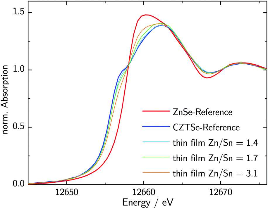 | ||
| Fig. 1 Edge-step normalized XANES spectra of Cu2ZnSnSe4 and ZnSe measured at the K-edge of Se together with the spectra of CZTSe thin film samples with varying Zn/Sn-ratios. | ||
These substantial differences in the XANES spectra of Cu2ZnSnSe4 and ZnSe enable the quantification of ZnSe as a secondary phase in CZTSe samples. The measured XANES spectra of specific thin-film samples with varying Zn/Sn-ratios are shown in Fig. 1. It can be clearly seen that the pre-edge feature, characteristic for CZTSe, varies systematically with the Zn/Sn-ratio. The pre-edge feature growths with increasing CZTSe content, while the first maximum at 12660 eV decreases according to the spectra being a superposition of the reference spectra. A linear combination analysis of a spectrum of one particular thin film sample is shown in Fig. 2. To be most sensitive to the distinct features of the reference spectra, the sample spectra are fitted within a range of −3 eV to 8 eV with respect to the absorption edge position. The linear combination of the CZTSe and ZnSe reference spectra shows the best fit with 35.5% ZnSe and 64.5% CZTSe and is in excellent agreement with the measured spectrum. Comparing two different spectra, the fits appear to be sensitive to a difference of roughly 3% in ZnSe-content. Nevertheless, the absolute error is slightly larger due to the choice of background subtraction and normalization parameters and is estimated to be around 5% absolute in ZnSe-content.
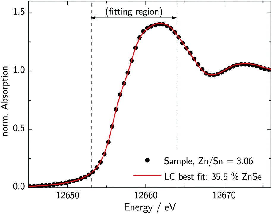 | ||
| Fig. 2 Measured and edge-step normalized XANES spectrum of the Se K-edge of one specific thin film CZTSe sample (dotted) together with a fit obtained by a linear combination of CZTSe and ZnSe reference spectra (red). | ||
Principal stability of single phase CZTS/CZTSe
Stoichiometric CZTS and CZTSe crystallize in the kesterite structure with 8 chalcogen atoms per unit cell.38,39 Correspondingly there are also 8 cations per unit cell, 4 Cu, 2 Zn and 2 Sn atoms. Deviations of the stoichiometry can be described as combinations of intrinsic point defects which can be antisite defects, vacancies and interstitials. Due to the comparably high enthalpy of formation for interstitial point defects,22,40,41 it can be assumed that macroscopic deviations from stoichiometry can be attributed to antisite defects and vacancies only. Assuming a completely occupied anion lattice, the following constraint is found for the cations just by considering the limited number of lattice sites:| S = Cu + Zn + Sn + V, | (1) |
| 2S = Cu + 2Zn + 4Sn. | (2) |
 | (3) |
Composition of the CZTS/Se phase
The total elemental sample composition as measured by XRF or EDX is a sum of compositions of the individual phases within a sample. For example, if we assume a sample to consist of CZTS, ZnS and CuxS, the Cu/Sn and Zn/Sn ratios of the CZTS phase are significantly lower than the corresponding ratios of the total sample as a result of Cu and Zn being bound in secondary phases. By quantitatively measuring the phase composition of a sample and combining this information with the total composition of the overall sample it is therefore possible to recalculate the actual composition of the CZTS/Se phase. The total sample compositions as determined by XRF in the case of CZTS and by EDX in the case of CZTSe are shown in Fig. 6 and 7, respectively. The given uncertainties are derived by Gaussian error propagation on the basis of a measurement uncertainty of 1 at%. For the CZTS samples shown in Fig. 6, the total sample compositions are found to lie in the Zn-rich and Cu-rich regions of the quasi ternary phase diagram, whereas for the CZTSe samples shown in Fig. 7 the total sample compositions are found to be Zn-rich located on the Cu-poor side of the ZnSe–Cu2SnSe3-tie line. These compositions are intentionally chosen to quantify CuxS and ZnS in CZTS while restricting the quantification to the ZnSe phase in CZTSe because of the limited spectral resolution at the Se K-edge.To reveal the composition of the CZTS phase in samples with different Cu/Sn and Zn/Sn-ratios, ZnS and CuxS are quantified by linear combination analysis of their XANES spectra as described elsewhere.14 ZnSe in CZTSe samples with different Zn/Sn-ratios is quantified as described above. The determined amounts of ZnS, ZnSe and CuxS in CZTS/CZTSe thin films are shown in Fig. 3–5 with respect to the Zn/Sn or Cu/Sn ratio of the total sample composition. In each sample the quantity of formed secondary phases strongly correlates with the total sample composition. For example, in Zn-rich samples (Zn/Sn > 1) the ratio of ZnS/ZnSe correlates directly with the Zn/Sn-ratio, while for Cu-rich samples with Cu/Sn > 2 the secondary phase CuxS is formed.
 | ||
| Fig. 3 Molar fraction of sulfur bound in ZnS in CZTS thin films with different Zn/Sn-ratios of the total sample composition as determined by XANES analysis at the K-edge of sulfur together with a fit to eqn (5) which determines the Zn/Sn-ratio of the remaining CZTS phase. | ||
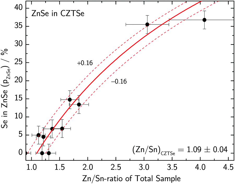 | ||
| Fig. 4 Molar fraction of selenium bound in ZnSe in CZTSe thin films with different Zn/Sn-ratios of the total sample composition as determined by XANES analysis at the K-edge of selenium together with a fit to eqn (5) which determines the Zn/Sn-ratio of the remaining CZTSe phase. | ||
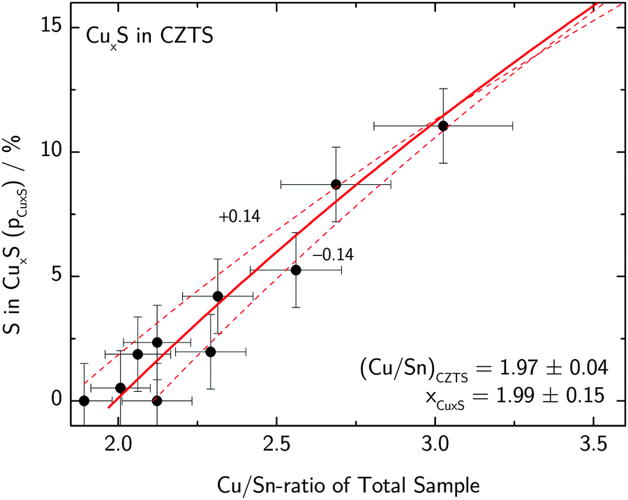 | ||
| Fig. 5 Fraction of sulfur bound in CuxS found in CZTS thin films with different Cu/Sn-ratios of the total sample composition as determined by XANES analysis at the K-edge of sulfur together with a fit to eqn (7) which determines the Cu/Sn-ratio of the remaining CZTS phase. | ||
To determine the amount of Zn which is consumed by ZnS/ZnSe, it is important to note that a linear combination analysis of the chalcogen K-edge spectra directly determines the percentage pX of chalcogen being bound in phase X with respect to the total amount of chalcogen atoms in the sample. The total amount of chalcogen in a CZTS/CZTSe sample is difficult to measure especially in the case of the sulfur compound due to the lack of reference samples and the strong matrix absorption of the S K-fluorescence lines. Instead the amount of chalcogen in the sample can be calculated from the metal composition taking the octet-rule into account, see eqn (2). In the following, the case of CZTS will be evaluated only, but all formulas also directly apply to the corresponding selenium containing compounds.
Assuming ZnS to be in stoichiometric composition the amount of chalcogen in ZnS equals the amount of Zn in ZnS. Therefore the amount of Zn in CZTS is given by:
| ZnCZTS = Zntotal − ZnZnS = Zntotal − pZnS·Stotal, | (4) |
Assuming a certain threshold composition of Zn/Sn = Z above which all excess Zn forms ZnS, it is possible to describe the formation of ZnS, pZnS, analytically by combining eqn (2) and (4):
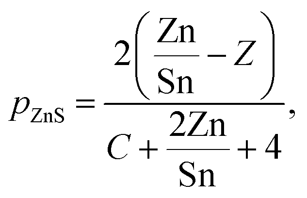 | (5) |
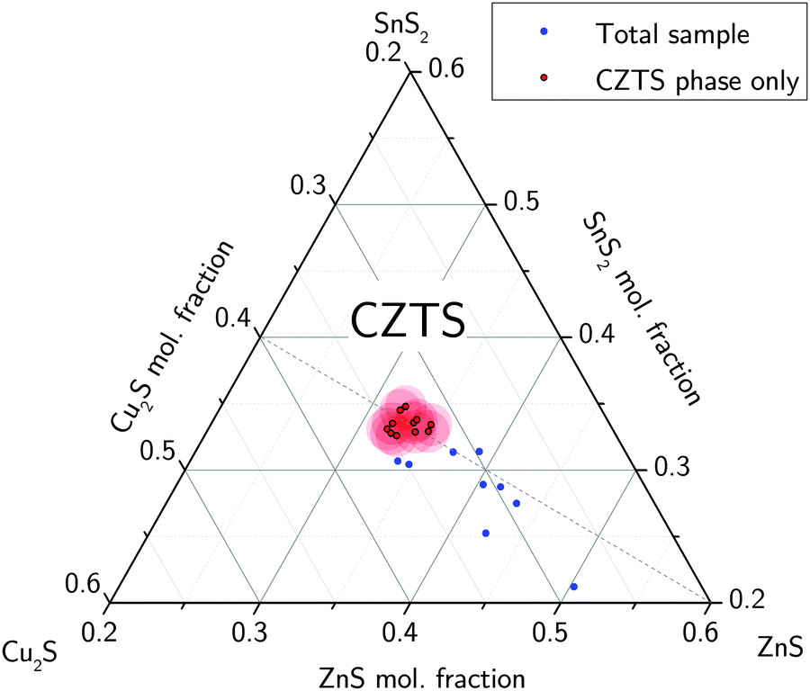 | ||
| Fig. 6 Total sample compositions of CZTS thin films as measured by XRF (blue) together with the actual composition of the CZTS-phase (red) as determined by a combination of XRF and XANES analysis. The uncertainty of the CZTS phase composition is shown in slightly transparent red circles. | ||
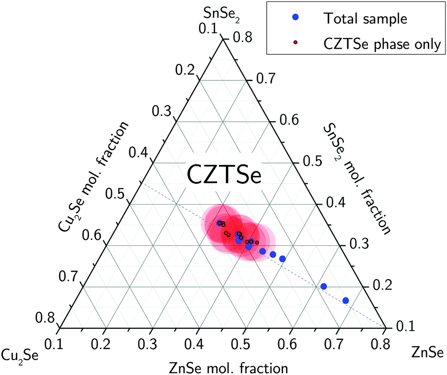 | ||
| Fig. 7 Total sample compositions of CZTSe thin films as measured by EDX (blue) together with the actual composition of the CZTSe-phase (red) as determined by a combination of EDX and XANES analysis. The uncertainty of the CZTSe phase composition is shown in slightly transparent red circles. | ||
The measured amount of copper sulfide in the same CZTS sample series as above is shown in Fig. 5 with respect to the Cu/Sn-ratio of the sample. Note that for samples where ZnS was also found, the amount of Zn and S which segregated in ZnS was subtracted from the sample composition as described above, such that pCuxS + pCZTS = 100%.
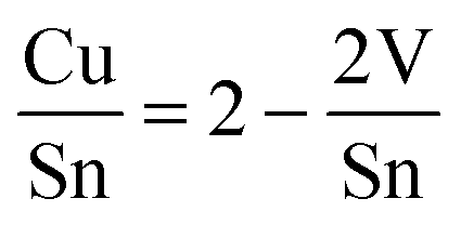
The amount of Cu in the CZTS phase is given by subtracting the copper which is consumed by CuxS from the total amount of copper:
| CuCZTS = Cutotal − CuCuxS = Cutotal − (2 − x)·pCuxS·Stotal | (6) |
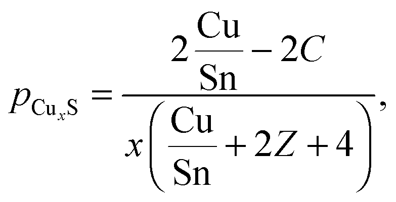 | (7) |
By subtracting copper and zinc which is segregated in the secondary phases CuxS, ZnS or ZnSe from the composition of the total sample using eqn (4) and (6) it is now possible to calculate the actual composition of the CZTS/CZTSe phase. Total sample compositions as well as the composition of the CZTS/CZTSe phase revealed by this analysis are shown together in Fig. 6 and 7, respectively. The uncertainty related to the determination of the CZTS/CZTSe composition is also shown. It was calculated by error propagation of the uncertainties of the XRF, EDX and XANES measurements. The shown uncertainty is a mean value of individual uncertainties determined for all used CZTS/CZTSe samples, respectively. It clearly can be seen that within the uncertainty, the composition of the CZTS or CZTSe phase coincides with the point of stoichiometry as it was determined by the least square fitting above. Therefore it can be concluded that it is not possible to form neither Cu-rich nor Zn-rich CZTS even if grown under Cu-rich or Zn-rich conditions, since in these cases excess copper or zinc will always segregate in secondary phases.
It has to be mentioned that it can be misleading to use the value of Cu/(Zn + Sn) to determine the Cu-richness of a sample, as is often done in the literature, because of the possible formation of ZnS. Most CZTS and CZTSe samples are synthesized in the Zn-rich region of the phase diagram and therefore exhibit ZnS segregations, which reduce the Zn-content of the CZTS/Se phase. Therefore the CZTS phase can be stoichiometric in copper even if the Cu/(Zn + Sn)-value is below one. Therefore we propose to use the Cu/Sn-ratio and the Zn/Sn-ratio to describe the sample composition and compare it with various electrical characterizations, as the Cu/Sn-value is unaffected by the formation of ZnS and thus reflects, more directly, the composition of the CZTS/Se phase.
Summary and conclusions
It was shown that ZnSe as a secondary phase in CZTSe thin film samples can be identified and quantified using X-ray near edge absorption spectroscopy at the K-edge of selenium. ZnSe and CZTSe single phase references show distinct features in the X-ray absorption near edge structure which enable the quantification of secondary phases in phase mixture systems by linear combination analysis. Due to a significant broadening of the absorption spectra at X-ray energies of the selenium K-edge, the quantification of ZnSe in CZTSe is not as precise as the quantification of ZnS in CZTS at the K-edge of sulfur, which has been demonstrated previously.14 We anticipate that with this method, ZnSe fractions down to at least 5% by volume can be quantified.It was shown that the segregation of ZnS, ZnSe or CuxS strongly correlates with the Zn/Sn and Cu/Sn-ratio of the total sample composition.
By a combination of X-ray absorption spectroscopy at the chalcogen K-edges of CZTS/CZTSe and X-ray fluorescence it was demonstrated that it is possible to determine the actual composition of the CZTS/Se phase in mixed phase thin film samples. The determined composition of the CZTS/Se phase significantly deviates from the total sample composition. The Zn/Sn-ratio of the CZTS and CZTSe phases was shown to be limited to around one for the case of Zn-rich sample compositions. As a result, all excess Zn within the sample segregates in ZnS/ZnSe as secondary phases.
Similarly, it was found that CuxS is formed in Cu-rich samples in such a way that the Cu/Sn-ratio of the CZTS phase is limited to two for Cu-rich total sample compositions. This shows that the single phase region of CZTS towards Cu-rich and Zn-rich compositions is rather small and coincides, within the measurement uncertainty, with the point of stoichiometry.
Conflict of interest
The authors declare no competing financial interest.Acknowledgements
We gratefully acknowledge the provision of beamtime by HASYLAB as well as the support at the beamlines by Edmund Welter, Michael Murphy and Adam Webb. Additionally, the authors would like to thank Lars Steinkopf at the HZB for providing substrates and support during the deposition of the samples.References
- T. Unold and H. W. Schock, Nonconventional (Non-Silicon-Based) Photovoltaic Materials, Annu. Rev. Mater. Res., 2011, 41, 297–321 CrossRef CAS.
- K. Ito, Copper Zinc Tin Sulfide-Based Thin Film Solar Cells, John Wiley & Sons, 2015 Search PubMed.
- K. Ito and T. Nakazawa, Electrical and Optical Properties of Stannite-Type Quaternary Semiconductor Thin Films, Jpn. J. Appl. Phys., 1988, 27, 2094 CrossRef CAS.
- S. Chen, A. Walsh, J.-H. Yang, X. G. Gong, L. Sun, P.-X. Yang, J.-H. Chu and S.-H. Wei, Compositional dependence of structural and electronic properties of CuZnSn(S,Se) alloys for thin film solar cells, Phys. Rev. B: Condens. Matter Mater. Phys., 2011, 83, 125201 CrossRef.
- W. Wang, et al. Device Characteristics of CZTSSe Thin-Film Solar Cells with 12.6% Efficiency, Adv. Energy Mater., 2014, 4, 1301465 Search PubMed.
- C. Persson, Electronic and optical properties of Cu2ZnSnS4 and Cu2ZnSnSe4, J. Appl. Phys., 2010, 107, 053710 CrossRef.
- D. M. Berg, et al. Discrimination and detection limits of secondary phases in Cu2ZnSnS4 using X-ray diffraction and Raman spectroscopy, Thin Solid Films, 2014, 569, 113–123 CrossRef CAS.
- M. Ganchev, et al. Phase composition of selenized Cu2ZnSnSe4 thin films determined by X-ray diffraction and Raman spectroscopy, Thin Solid Films, 2011, 519, 7394–7398 CrossRef CAS.
- P. A. Fernandes, P. M. P. Salomé and A. F. da Cunha, Growth and Raman scattering characterization of Cu2ZnSnS4 thin films, Thin Solid Films, 2009, 517, 2519–2523 CrossRef CAS.
- A. Redinger, et al. Detection of a ZnSe secondary phase in coevaporated Cu2ZnSnSe4 thin films, Appl. Phys. Lett., 2011, 98, 101907 CrossRef.
- E. A. Lund, H. Du, W. M. H. Oo, G. Teeter and M. A. Scarpulla, Investigation of combinatorial coevaporated thin film Cu2ZnSnS4(II): Beneficial cation arrangement in Cu-rich growth, J. Appl. Phys., 2014, 115, 173503 CrossRef.
- M. Grossberg, et al. Photoluminescence and Raman study of Cu2ZnSn(SexS1 − x)4 monograins for photovoltaic applications, Thin Solid Films, 2011, 519, 7403–7406 CrossRef CAS.
- X. Fontané, et al. In-depth resolved Raman scattering analysis for the identification of secondary phases: Characterization of Cu2ZnSnS4 layers for solar cell applications, Appl. Phys. Lett., 2011, 98, 181905 CrossRef.
- J. Just, D. Lützenkirchen-Hecht, R. Frahm, S. Schorr and T. Unold, Determination of secondary phases in kesterite Cu2ZnSnS4 thin films by X-ray absorption near edge structure analysis, Appl. Phys. Lett., 2011, 99, 262105 CrossRef.
- K. C. Mills, Thermodynamic data of Sulphides, Selenides and Tellurides, Butterworths, London, 1974 Search PubMed.
- B. Shin, et al. Thin film solar cell with 8.4% power conversion efficiency using an earth-abundant Cu2ZnSnS4 absorber, Prog. Photovoltaics, 2013, 21, 72–76 CAS.
- I. Repins, et al. Co-evaporated Cu2ZnSnSe4 films and devices, Sol. Energy Mater. Sol. Cells, 2012, 101, 154–159 CrossRef CAS.
- J. J. Scragg, et al. Rapid annealing of reactively sputtered precursors for Cu2ZnSnS4 solar cells, Prog. Photovoltaics, 2014, 22, 10–17 CAS.
- A. Redinger and S. Siebentritt, Coevaporation of Cu2ZnSnSe4 thin films, Appl. Phys. Lett., 2010, 97, 092111 CrossRef.
- H. Katagiri, K. Jimbo, M. Tahara, H. Araki and K. Oishi, The influence of the composition ratio on CZTS-based thin film solar cells, Mater. Res. Soc. Symp. Proc. 2009, 1165, M04-01.
- V. Kosyak, M. A. Karmarkar and M. A. Scarpulla, Temperature dependent conductivity of polycrystalline Cu2ZnSnS4 thin films, Appl. Phys. Lett., 2012, 100, 263903 CrossRef.
- S. Chen, A. Walsh, X.-G. Gong and S.-H. Wei, Classification of Lattice Defects in the kesterite Cu2ZnSnS4 and Cu2ZnSnSe4 Earth-Abundant Solar Cell Absorbers, Adv. Mater., 2013, 25, 1522–1539 CrossRef CAS PubMed.
- I. D. Olekseyuk, I. V. Dudchak and L. V. Piskach, Phase equilibria in the Cu2S–ZnS–SnS2 system, J. Alloys Compd., 2004, 368, 135–143 CrossRef CAS.
- A. Lafond, L. Choubrac, C. Guillot-Deudon, P. Deniard and S. Jobic, Crystal Structures of Photovoltaic Chalcogenides, an Intricate Puzzle to Solve: the Cases of CIGSe and CZTS Materials, Z. Anorg. Allg. Chem., 2012, 638, 2571–2577 CrossRef CAS.
- L. Choubrac, A. Lafond, C. Guillot-Deudon, Y. Moëlo and S. Jobic, Structure Flexibility of the Cu2ZnSnS4 Absorber in Low-Cost Photovoltaic Cells: From the Stoichiometric to the Copper-Poor Compounds, Inorg. Chem., 2012, 51, 3346–3348 CrossRef CAS PubMed.
- B.-A. Schubert, et al. Cu2ZnSnS4 thin film solar cells by fast coevaporation, Prog. Photovoltaics, 2011, 19, 93–96 CAS.
- V. A. Solé, E. Papillon, M. Cotte, P. Walter and J. Susini, A multiplatform code for the analysis of energy-dispersive X-ray fluorescence spectra, Spectrochim. Acta, Part B, 2007, 62, 63–68 CrossRef.
- T. Ericson, T. Kubart, J. J. Scragg and C. Platzer-Björkman, Reactive sputtering of precursors for Cu2ZnSnS4 thin film solar cells, Thin Solid Films, 2012, 520, 7093–7099 CrossRef CAS.
- E. Welter, Beamline A1 - Hasylab. AIP Conf Proc 955, 2010.
- W. Ki and H. W. Hillhouse, Earth-Abundant Element Photovoltaics Directly from Soluble Precursors with High Yield Using a Non-Toxic Solvent, Adv. Energy Mater., 2011, 1, 732–735 CrossRef CAS.
- C. M. Sutter-Fella, et al. Sodium Assisted Sintering of Chalcogenides and Its Application to Solution Processed Cu2ZnSn(S,Se)4 Thin Film Solar Cells, Chem. Mater., 2014, 26, 1420–1425 CrossRef CAS.
- S. Schorr, H.-J. Hoebler and M. Tovar, A neutron diffraction study of the stannite-kesterite solid solution series, Eur. J. Mineral., 2007, 19, 65–73 CrossRef CAS.
- R. Frahm, Beamline X – Hasylab, Rev. Sci. Instrum., 1989, 60, 2515–2518 CrossRef CAS.
- B. L. Henke, E. M. Gullikson and J. C. Davis, X-ray interactions: photoabsorption, scattering, transmission, and reflection at E = 50–30000 eV, Z = 1–92, At. Data Nucl. Data Tables, 1993, 54, 181–342 CrossRef CAS.
- M. O. Krause and J. H. Oliver, Natural widths of atomic K and L levels, Kα X-ray lines and several KLL Auger lines, J. Phys. Chem. Ref. Data, 1979, 8, 329–338 CrossRef CAS.
- M. Newville, IFEFFIT: interactive XAFS analysis and FEFF fitting, J. Synchrotron Radiat., 2001, 8, 322–324 CrossRef CAS PubMed.
- B. Ravel and M. Newville, ATHENA, ARTEMIS, HEPHAESTUS: data analysis for X-ray absorption spectroscopy using IFEFFIT, J. Synchrotron Radiat., 2005, 12, 537–541 CrossRef CAS PubMed.
- S. R. Hall, J. T. Szymanski and J. M. Stewart, Kesterite, Cu2(Zn,Fe)SnS4, and stannite, structurally similar but distinct minerals, Can. Mineral., 1978, 16, 131–137 CAS.
- S. Schorr, The crystal structure of kesterite type compounds: A neutron and X-ray diffraction study, Sol. Energy Mater. Sol. Cells, 2011, 95, 1482–1488 CrossRef CAS.
- S. Chen, J.-H. Yang, X. G. Gong, A. Walsh and S.-H. Wei, Intrinsic point defects and complexes in the quaternary kesterite semiconductor Cu2ZnSnS4, Phys. Rev. B: Condens. Matter Mater. Phys., 2010, 81, 245204 CrossRef.
- D. Han, et al. Deep electron traps and origin of p-type conductivity in the earth-abundant solar-cell material Cu2ZnSnS4, Phys. Rev. B: Condens. Matter Mater. Phys., 2013, 87, 155206 CrossRef.
Footnotes |
| † Electronic supplementary information (ESI) available. See DOI: 10.1039/c6cp00178e |
| ‡ Present address: Electrical Engineering and Computer Sciences, University of California, Berkeley, California 94720, USA. |
| This journal is © the Owner Societies 2016 |