
 Open Access Article
 This Open Access Article is licensed under a
 Creative Commons Attribution 3.0 Unported Licence
YSZ thin films with minimized grain boundary resistivity†
Edmund M.
Mills
a,
Matthias
Kleine-Boymann
b,
Juergen
Janek
b,
Hao
Yang
c,
Nigel D.
Browning
c,
Yayoi
Takamura
a and
Sangtae
Kim
*a
aUniversity of California Davis, Department of Chemical Engineering and Materials Science, 3001 Ghausi Hall, Davis California 95616, USA. E-mail: chmkim@ucdavis.edu
bJustus-Liebig-Universität Gießen, Physikalisch-Chemisches Institut, Heinrich-Buff-Ring 58, 35392 Gießen, Germany
cPacific Northwest National Laboratory, 902 Battelle Boulevard, Richland, WA, USA
First published on 31st March 2016
Abstract
In recent years, interface engineering of solid electrolytes has been explored to increase their ionic conductivity and improve the performance of solid oxide fuel cells and other electrochemical power sources. It has been observed that the ionic conductivity of epitaxially grown thin films of some electrolytes is dramatically enhanced, which is often attributed to effects (e.g. strain-induced mobility changes) at the heterophase boundary with the substrate. Still largely unexplored is the possibility of manipulation of grain boundary resistivity in polycrystalline solid electrolyte films, clearly a limiting factor in their ionic conductivity. Here we report that the ionic conductivity of yttria stabilized zirconia thin films with nano-columnar grains grown on a MgO substrate nearly reaches that of the corresponding single crystal when the thickness of the films becomes less than roughly 8 nm (smaller by a factor of three at 500 °C). Using impedance spectroscopy, the grain boundary resistivity was probed as a function of film thickness. The resistivity of the grain boundaries near the film–substrate interface and film surface (within 4 nm of each) was almost entirely eliminated. This minimization of grain boundary resistivity is attributed to Mg2+ diffusion from the MgO substrate into the YSZ grain boundaries, which is supported by time of flight secondary ion mass spectroscopy measurements. We suggest grain boundary “design” as an attractive method to obtain highly conductive solid electrolyte thin films.
Introduction
Solid oxide fuel cells (SOFCs) are electrochemical devices that convert chemical energy into electrical energy.1 Central to SOFC operation is the electrolyte, which lies between the anode and cathode where redox half-reactions occur. In order for the fuel (e.g. H2) to be oxidized at the anode, the electrolyte must allow sufficient ion diffusion so that the two half-reactions can be linked to complete the full reaction. Therefore ionic conductivity is the critical material property for electrolytes. Over the past decades various approaches have been taken to improve the ionic conductivity of electrolyte materials including exploration of novel materials, compositional optimization, and more recently, interface engineering.2Interface engineering shows promise for improving the ionic conductivity of electrolytes and performance of SOFCs.3,4 The local structural, electrical, and chemical properties of interfaces between two different materials, i.e. hetero-interfaces, or between two chemically identical materials, e.g. grain boundaries, deviate from those of the corresponding crystalline bulk. Consequently, the defect concentration and dynamics of ionic motion parallel to and perpendicular to the interface may be altered. For example, it has been known that in some prominent oxide- or proton-conducting solid electrolytes, ions are depleted to form a space charge region in the vicinity of the grain boundary core, leading to obstruction of ion transport across the grain boundaries and thus limiting the ionic conductivity of polycrystalline electrolytes (frequently designated as the space charge effect).5,6 On the other hand, interfaces may also be beneficial; considerable enhanced ionic conductivity relative to bulk materials has been observed at the hetero-interface of yttria stabilized zirconia (YSZ) thin film and a MgO substrate.7 Extensive efforts have been made to utilize such an “enhancement” effect in the design of advanced electrolyte materials with high ionic conductivity, e.g. through grain boundary modification8 or the design of composite materials.9
In recent years, there have been multiple reports of dramatically enhanced ionic conductivity in epitaxial thin film electrolytes.7,10,11 Different sources of this effect have been proposed, including strain,12 misfit dislocations,13 and disorder in the oxygen sub-lattice at the hetero-interface in thin films.11 It has been demonstrated that strain has a sizeable effect on the ionic conductivity of YSZ thin films, through modifying the volume available for oxygen-ion hopping, with compressive strain reducing conductivity and tensile strain enhancing it. Nevertheless, due to the variety of microstructures in thin films, the effect of other structural features and their interactions have yet to be untangled; the ionic conductivity may be modified by additional mechanisms.14
Grain boundaries are often formed during the growth of YSZ and other electrolyte thin films due to structural differences between the film and substrate, leading to polycrystalline – mostly even nanocrystalline films.15 As these grain boundaries are highly resistive to ionic conduction, the enhancement observed in epitaxial films can be nullified in polycrystalline films. Additionally, grain boundaries may relieve strain, reducing ionic conductivity enhancements due to strain.12 Research on the effect of grain boundaries on the ionic conductivity of thin films has begun, for example, examining the effect of grain orientation and grain boundary coherence on thin film ionic conductivity.16 One area yet to be explored is the intersection of grain boundaries and the hetero-interface between the thin film and the substrate. This is of practical importance, as such intersections will be relevant when attempting to utilize the thin film interface effect in SOFCs. If the high grain boundary resistivity at this point is unaltered, it will limit the conductivity of the electrolyte and obstruct the attempt to improve the ionic conductivity.
To investigate the ionic conductivity of grain boundaries near the hetero-interface, we synthesized YSZ thin films with nano-columnar grains and characterized their electrical properties using impedance spectroscopy. The thickness was varied to gain insight into the evolution of the ionic conductivity over the film thickness. The grain boundary resistance near the interface and extending approx. 8 nm into the film is almost completely eliminated; the thinnest nano-crystalline films show ionic conductivity comparable to single crystal YSZ. We attribute this reduction in grain boundary resistance to diffusion of Mg2+ from the substrate into the grain boundary cores. We us time of flight secondary ion mass spectrometry (ToF-SIMS) measurements to confirm diffusion of Mg2+ into the films, primarily along the grain boundaries.
Experimental
Pulsed laser deposition
YSZ thin films with thicknesses ranging from 4 to 900 nm were grown on (001)-oriented single crystal MgO substrates by pulsed laser deposition (PLD) using a KrF excimer laser with 248 nm wavelength. Films were grown from an 8YSZ target made with Tosoh YSZ powder. During growth, the substrate temperature was held at 700 °C and the oxygen pressure at 14 mTorr. A laser energy of 1.8 J cm−2 and a pulse rate of 5 Hz was used. Samples were cooled in 300 Torr oxygen pressure.X-ray diffraction and reflectivity
X-ray characterization was performed using a Bruker D8 Discover four-circle diffractometer utilizing Cu Kα1 radiation. The layer thickness, density, and roughness were determined by fitting the X-ray reflectivity (XRR) spectra using Bruker Leptos software.17Scanning transmission electron microscopy (STEM)
Aberration corrected FEI Titan (scanning) transmission electron microscopy was used to study the YSZ/MgO interface structure. The electron beam energy was 300 keV. STEM Z-contrast images were recorded using a high angle annular dark field (HAADF) detector. Cross section TEM specimen was prepared by mechanical grinding and ion milling using Gatan Precision Ion Polishing System.Time of flight secondary ion mass spectrometry (ToF-SIMS)
ToF-SIMS was performed using an ION-TOF TOF.SIMS V equipped with a 25 keV Bi primary ion gun and an O2 ion sputter gun. Depth profiles were measured in non-interlaced mode. For the 200 nm films the sputter gun was operated at 1 keV, for the 20 nm films it was set to 0.5 keV in order to adjust the erosion rate for the thinner film. The crater size was set to 200 × 200 μm² with an analysis area of 50 × 50 μm2 aligned in the center of the sputter crater. The total sputter dose did not exceed 2.4 × 10¹⁵ for both films.Impedance spectroscopy
Parallel platinum electrodes were sputtered onto the surface of the thin films, separated by 500 μm. Impedance spectroscopy measurements were carried out under air in the temperature range of 400–700 °C, using a Novocontrol Alpha-AN modulus analyzer in the frequency range from 10−1 to 107 Hz. Scribner Z-view was used to fit the data with an equivalent circuit composed of a resistor and capacitor in parallel. A custom MATLAB script was used to fit the conductivity data across all films and temperatures using a least squares method, discussed in more detail further on.Results and discussion
Thin film microstructure
Fig. 1(a) is an STEM Z-contrast image of a 20 nm thick YSZ film. The film has a columnar microstructure with an average grain diameter of 8.1 nm. Fig. 1(b) is a higher magnification STEM image showing the film/substrate interface, relative orientations of the grains, and a grain boundary. The STEM micrographs, along with the X-ray diffraction characterization (XRD), show that the films are fully crystalline with (111)-texture. The grains have four different in plane orientations with fourfold symmetry, with the YSZ〈11![[2 with combining macron]](https://www.rsc.org/images/entities/char_0032_0304.gif) 〉 directions parallel to the MgO〈110〉 directions. The film/substrate interface is sharp, without the presence of secondary phases. From XRR, it was determined that for all films, both the surface and interface have roughness less than one unit cell. Misfit dislocations have formed at the interface to fully relax the epitaxial strain. XRR indicated that the films had densities between 5.8 and 6.1 g cm−3, between 95% and 100% of theoretical density. Structural characterization shows the films are of high quality, and have a large number of vertical grain boundaries.
〉 directions parallel to the MgO〈110〉 directions. The film/substrate interface is sharp, without the presence of secondary phases. From XRR, it was determined that for all films, both the surface and interface have roughness less than one unit cell. Misfit dislocations have formed at the interface to fully relax the epitaxial strain. XRR indicated that the films had densities between 5.8 and 6.1 g cm−3, between 95% and 100% of theoretical density. Structural characterization shows the films are of high quality, and have a large number of vertical grain boundaries.
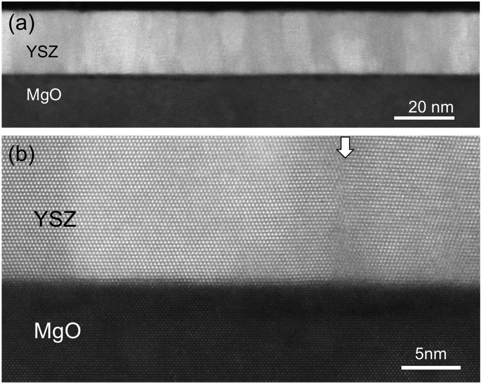 | ||
| Fig. 1 STEM HAADF images of a 20 nm YSZ thin film on a MgO substrate. (a) The low-mag image shows that the YSZ film has a nano-columnar microstructure with approximately 8.1 nm grain diameter and grain boundaries forming between grains. (b) High resolution image shows the relative crystal orientations between film and substrate, and the arrow indicates the presence of a grain boundary. | ||
Impedance characterization
The in-plane oxygen-ion conductivity of the films was then characterized with ac-impedance spectroscopy. Impedance spectroscopy uses the frequency domain to characterize different electrical processes in the sample, each with different characteristic frequency. The impedance spectra of a polycrystalline or nanocrystalline electrolyte is expected to appear as two semicircles when plotted as a Nyquist plot, representing charge transport in the bulk and grain boundary (ignoring electrode effects). However, as seen in Fig. 2(a), the impedance spectra of the YSZ thin films show only a single arc, due to the effect of the stray substrate capacitance: the substrate acts as a capacitor in parallel with the film, allowing the ac current to bypass the film at high frequencies due to the substrate's relatively high capacitance. This obscures the film's high frequency capacitive behavior and prevents the bulk and grain boundary contributions to the total impedance from being distinguished. The total resistance and substrate capacitance of each film were determined by fitting the impedance spectra with an equivalent circuit, composed of a resistor and constant phase element in parallel, corresponding to the film resistance and substrate capacitance, respectively. The measured capacitance for each sample was ∼2 × 10⁻¹² F, consistent with the expected stray substrate capacitance. Due to the large number of grain boundaries in the film, the bulk resistance is expected to be small compared to the grain boundary resistance. Therefore, the total resistance is controlled by the grain boundary resistance, and the electrical properties of the grain interiors are obscured.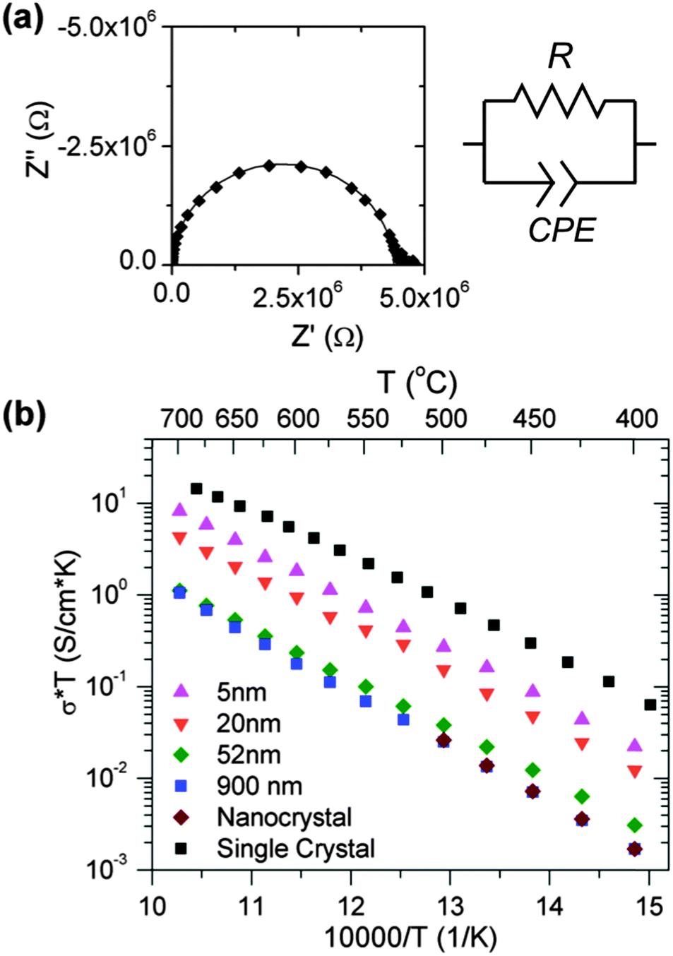 | ||
| Fig. 2 (a) A representative impedance spectrum of the YSZ thin films, of a 20 nm film at 500 °C. The impedance spectrum is composed of a single semi-circular arc corresponding to the film's impedance. Due to the sample geometry, the electrode contribution is small compared to that of the film. The spectrum has been fit by the equivalent circuit shown to the right, composed of a resistor and constant phase element in parallel. (b) An Arrhenius plot of the conductivity of representative thin films. As the film thickness is reduced, the conductivity increases from that of a nano-crystalline sample to close to that of a single-crystalline sample. | ||
Fig. 2(b) is an Arrhenius plot showing the total conductivity of representative films, from 400 °C to 700 °C. Also included in Fig. 2(b) are the bulk conductivity of YSZ (i.e. the conductivity equivalent to that of a YSZ single crystal) and total conductivity of a nanocrystalline YSZ (10 nm grains) ceramic for comparison. The latter is substantially lower than the former since it is almost entirely governed by the grain boundaries which block the ionic current in YSZ. The conductivity of the thicker films is consistent with that of the nanocrystalline ceramic as anticipated. However, as the film thickness decreases from 900 to 4 nm, the total conductivity of the film increases by approximately an order of magnitude.
Dependence of the impedance on film thickness
The relationship between the film thickness and conductivity can be understood with reference to the model shown in Fig. 3. The film is divided into two regions: a region of enhanced conductivity near the hetero-interface with thickness δ, and the remainder of the film with thickness d–δ. The resistance Rf corresponds to the total resistance of the film in this region, which is dominated by the grain boundary resistance. Ri corresponds to the resistance of the interfacial region. The two regions serve as parallel conduction pathways, represented by the equivalent circuit (Fig. 3). Their relative contributions to the total conductivity is determined by f, the fraction of the film composed by the interfacial region, δ/d. In the thicker films, with low f, the hetero-interface plays little role in the total conductivity of the films, such that conductivity similar to that of the corresponding nanocrystalline ceramic is observed. As f increases, the hetero-interface becomes more significant, and the total conductivity increases. When f reaches unity, when the film thickness is thinner than δ, the conductivity is determined solely by the interfacial region and is independent of thickness.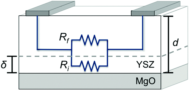 | ||
| Fig. 3 A schematic of the model used to understand the thickness dependence of the conductivity of the thin films. The film is divided into a region close to the interface with enhanced conductivity and the remainder of the film. The two regions contribute to the total conductivity as parallel conduction pathways. | ||
The behavior predicted by the model is readily apparent in Fig. 4(a), a plot of the conductivity vs. film thickness for representative temperatures. Here, in addition to the increase in conductivity with decreasing film thickness, a distinct plateau region is observed in the thinnest films.
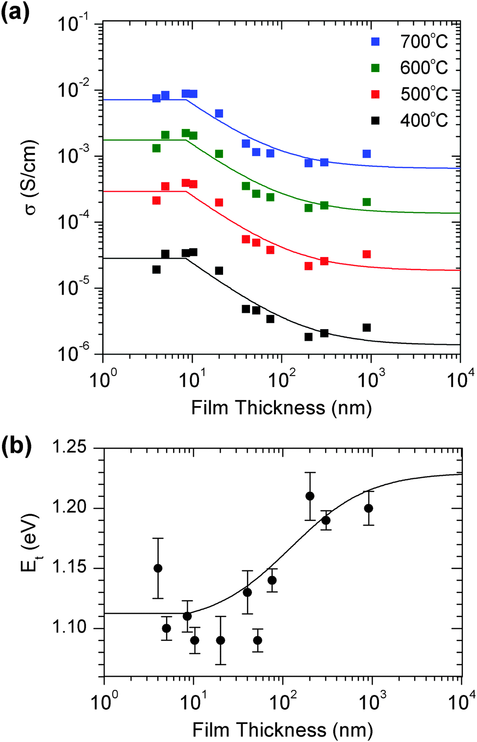 | ||
| Fig. 4 (a) A plot of the conductivity vs. film thickness for different temperatures. The conductivity increases as the film thickness is reduced, up to a limiting value. The fit of the model discussed is represented with solid lines, and fits the experimental data well. (b) A plot of the total activation energy Et of the films vs. film thickness. Again, the data are fit well by the model, again shown with the solid line. | ||
Using this model, the total conductivity of the film (σt) can be expressed quantitatively as
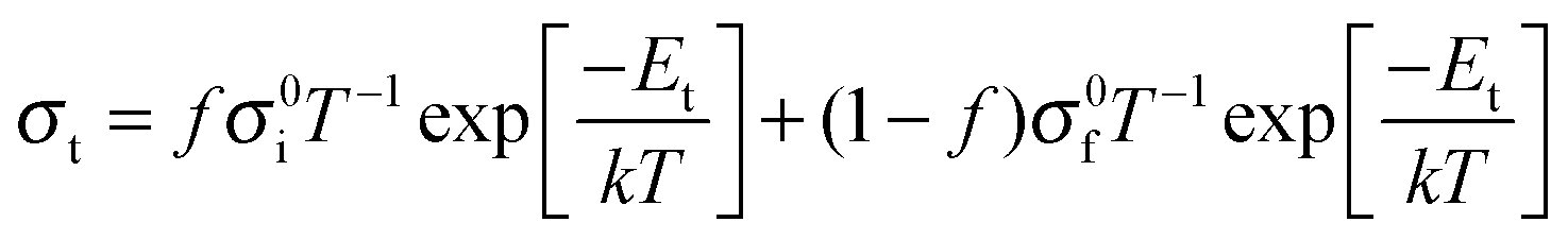 | (1) |
The activation energy of the film's total conductivity, Et, has been determined from the slope of the Arrhenius plot and is plotted in Fig. 4(b), with the activation energy for nanocrystalline YSZ as a reference. A decrease in Et is observed in the thinner films, as f is increased, with Et reaching Ei in the thinnest films. Using the results of the fit previously discussed, Et was determined from the temperature dependence of the predicted σt and are shown as the solid line. It is apparent that eqn (1) reproduces the change in Et with d reasonably well. The decrease in Et in the thinner films results from a lower activation energy in the regions of enhanced conductivity near the films' hetero-interface and surface.
Summarizing the results from the impedance characterization, we found that σt of the films was increased near the hetero-interface by an order of magnitude. In this region of thickness of δ, the grain boundary resistivity is significantly lower than in the rest of the film. The activation energy is also lower, whether due to a decrease in the grain boundary activation energy or an increased contribution of the bulk conductivity. The region of enhanced conductivity has a thickness of 7.6 nm. No structural differences extending roughly to δ, or 7.6 nm from the interface into the film could be identified from STEM. It is also unlikely that this effect is caused by a space-charge region at the hetero-interface, as the space-charge thickness in 8YSZ is less than 1 nm, or by structural differences immediately at the interface like misfit dislocations, as the extent of these effects is much smaller than δ.
Mg2+ diffusion into the grain boundary cores
We hypothesize that the grain boundary resistivity is reduced by the diffusion of Mg2+ from the MgO substrate into the grain boundary cores. Extrapolating from literature values for the diffusivity of Mg2+ in the bulk and grain boundaries of ZrO2 measured between 800 and 1000 °C, we anticipate that that Mg2+ could readily diffuse in the grain boundary cores but not in the grain interior at 700 °C, the highest temperature reached during thin film growth.18 This could modify the grain boundary resistivity: as mentioned earlier, the space charge effect may play a significant role in the high grain boundary resistivity of the YSZ films. Segregation of Mg2+ into the grain boundary core may result in reduction of the space-charge potential, leading to reduction in the grain boundary resistivity. This is also expected to lead to a reduction in the activation energy in these regions, as is evident in Fig. 4. This hypothesis is supported by previous research: Avila-Predes and Kim19 have demonstrated that segregation of metal cation impurities to the grain boundary cores in Gd-doped CeO2, a material similar to YSZ, reduces the grain boundary resistivity by up to an order of magnitude, while slightly reducing the activation energy. Litzelman et al.20 investigated the heterogeneous doping of nanocrystalline ceria thin films with Mg from a MgO substrate and an associated decrease in electronic conductivity. This was attributed to a reduction in the grain boundary potential, reducing the concentration of electrons in the grain boundary's space charge regions. For ionic conducting films, such a reduction of grain boundary potential would instead reduce the grain boundary resistance by reducing the potential barrier to oxygen vacancy migration across the grain boundaries. Thirdly, Suresh & Johnson21 reported an increase in the total conductivity of YSZ with Mg2+ doping, along with segregation of Mg2+ to the grain boundaries.To investigate whether such Mg2+ diffusion occurred in the YSZ thin films, ToF-SIMS was used to examine the distribution of Mg in 20 nm and 200 nm films. For comparison, reference films of the same thickness were deposited at room temperature by PLD. Mg2+ diffusion in these films is expected to be minimal due to the low deposition temperature and the lack of grain boundaries in the amorphous films. The hetero-interface was determined to be sharp by XRR. For both thicknesses, the Mg2+ profile extended further into the film from the interface region for the YSZ films deposited at 700 °C than the room temperature sample (Fig. 5). Therefore, the conclusion that Mg2+ diffuses into the film's grain boundary cores during film deposition is validated by the ToF-SIMS depth profiling measurements.
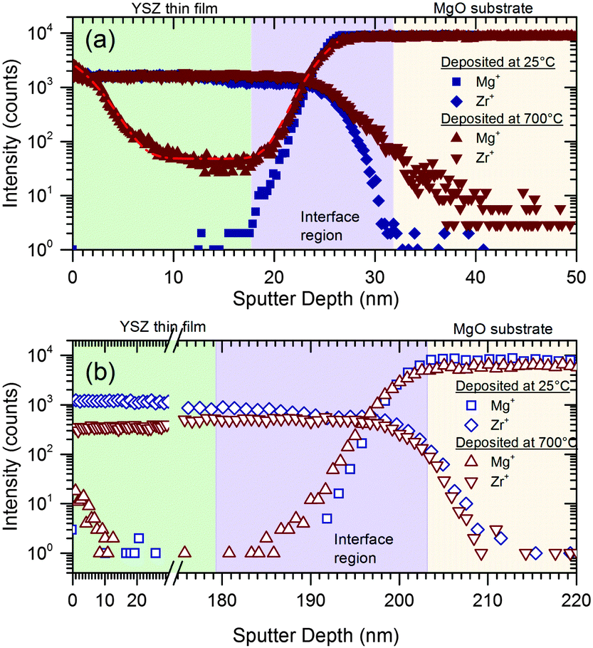 | ||
| Fig. 5 ToF-SIMS depth profile of the Mg+ and Zr+ secondary ion signal from (a) two 20 nm YSZ thin films as well as (b) two 200 nm thin films on MgO substrates. The depth scale is referring to the films deposited at 25 °C. The depth profiles of the thin films deposited at 700 °C were shifted, so that the interface regions in all depth profiles are aligned graphically in order to illustrate the differences in the depth profiles. The samples deposited at 700 °C (red triangles) show Mg diffusion into the YSZ thin films in the near interface region for both, the 200 nm and the 20 nm thin films. The red dashed and dash-dotted line are the fitted diffusion profiles at the interface and the surface respectively for the 20 nm sample. | ||
In addition to the diffusion from the interface, the depth profiles show Mg enrichment at the YSZ surface. We attribute this surface enrichment to fast surface diffusion of Mg2+ up the side of the films, across the film surface, and subsequent diffusion into the films’ grain boundaries, giving the observed depth profiles. The possibility of diffusion from the substrate through the grain boundaries and subsequent segregation at the surface can be eliminated, as the 200 nm films show significant Mg enrichment at the surface with undetectable Mg concentrations throughout the major part of the film. We expect that the Mg enrichment near the film surface, along with that at the hetero-interface, will reduce the local grain boundary resistance, giving rise to two regions of enhanced conductivity.
Having seen significant diffusion of Mg into the films, we can now compare the extent of Mg diffusion (i.e. the diffusion length) to δ, the thickness of the region of enhanced conductivity calculated from the conductivity measurements. The interfacial and surface profile were fitted with the infinite source solution for Fick's law to the ToF-SIMS data with a non-linear least mean square Levenberg–Marquardt routine, yielding diffusion lengths of 3.9 (±0.2) nm and 4.0 (±0.1) nm for diffusion from the interface and surface, respectively. This gives a combined diffusion length for Mg diffusion into the films of 7.9 nm, very close to the value calculated for δ of 7.6 nm. The adjusted R2 of the diffusion profiles was R2 = 0.995 for both interface and surface region.
Although the diffusion profiles at both the surface and the substrate interface are quite narrow, we tried to verify the presence of grain boundary diffusion by analysing the profiles with Whipple's solution for grain boundary diffusion, through plotting ln(I) vs. y6/5 for the 20 nm and 200 nm sample (see ESI†). Here I represents the measured intensity of Mg+ signal, neglecting matrix effects, proportional to the concentration of Mg cations and y represents the diffusion depth with respect to the interface under investigation. If diffusion from the MgO substrate primarily takes place in the grain boundaries, the profile gives a straight line for ln(I) vs. y6/5.22 At the surface of the 20 nm sample, the plot versus y6/5 indeed shows a linear course in the surface region. However, the interface diffusion profile does not show linear behaviour. The same holds for the interface profile of the 200 nm sample. The Mg intensity at the 200 nm sample surface was to narrow for any analysis. We conclude that there is clear evidence of grain boundary diffusion from the surface, but the mechanism of the diffusion from the substrate remains unclear. In view of the restricted data set, we consider these results with care and take this as highly interesting motivation to extend the diffusion studies and their analysis by SIMS. Thus, in order to gain deeper insight into the diffusion of Mg into the YSZ thin films further studies are required and planned. Notwithstanding, the width of the region of significant Mg concentration the diffusion length 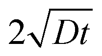 obtained from the infinite source solution is a good measure in order to quantify the thickness of the Mg enriched region – irrespective of the details of the quantitative analysis of the profiles. The good agreement between the two, the proposed model and the ToF-SIMS measurements provides strong evidence that the Mg diffusion is the source of the reduced grain boundary resistance and enhanced conductivity observed in these thin films.
Conclusions
In summary, thin films with nano-columnar grains were deposited and characterized. The conductivity in the thinnest films was enhanced by an order of magnitude relative to the thicker films and comparable to that of single crystal YSZ. The enhanced conductivity was attributed to a reduction of the grain boundary resistivity near the thin film interface in a region of roughly 8 nm. Based on this length-scale, surface and interfacial space-charge effects and structural differences were eliminated as the source of reduced grain boundary resistivity. We attribute the enhancement in conductivity to diffusion of Mg2+ from MgO substrate into the grain boundaries, which was verified by ToF-SIMS depth profiling. Future work in extending this effect to thicker films or bulk materials appears promising. These results demonstrate the importance of grain boundaries in understanding the ionic conductivity of electrolyte thin films, as well as the mitigation of their blocking effect due to chemical diffusion near the hetero-interface.Acknowledgements
We gratefully acknowledge many valuable discussions about ToF-SIMS measurements with Dr Marcus Rohnke. S. K. wishes to thank the US-Israel Binational Science Foundation for funding this research. Y. T. would like to acknowledge NSF for financial support (DMR 747896). JJ and MKB acknowledge financial support by DFG (Deutsche Forchungsgemeinschaft) within the project DFG Ja 648/21-1. N. B. acknowledges support through the Laboratory Directed Research and Development (LDRD) Program Chemical Imaging Initiative (CII) at Pacific Northwest National Laboratory (PNNL) and the Environmental Molecular Sciences Laboratory (EMSL), a national scientific user facility sponsored by DOE's Office of Biological and Environmental Research (BER) at PNNL. PNNL is a multiprogram national laboratory operated by Battelle for DOE under Contract DE-AC05-76RL01830.Notes and references
- E. D. Wachsman and K. T. Lee, Science, 2011, 334, 935–939 CrossRef CAS PubMed.
- H. Aydin, C. Korte, M. Rohnke and J. Janek, Phys. Chem. Chem. Phys., 2013, 15, 1944–1955 RSC.
- E. Fabbri, D. Pergolesi and E. Traversa, Sci. Technol. Adv. Mater., 2010, 11, 054503 CrossRef.
- B. Zhu, Int. J. Energy Res., 2009, 33, 1126–1137 CrossRef CAS.
- X. Guo and J. Maier, J. Electrochem. Soc., 2001, 148, E121 CrossRef CAS.
- X. Guo and R. Waser, Prog. Mater. Sci., 2006, 51, 151–210 CrossRef CAS.
- C. Korte, N. Schichtel, D. Hesse and J. Janek, Monats. Chem. – Chemical Monthly, 2009, 140, 1069–1080 CrossRef CAS PubMed.
- S. Jiang and J. B. Wagner Jr, J. Phys. Chem. Solids, 1994, 56, 1101–1111 CrossRef.
- X. Wang, Y. Ma, S. Li, A.-H. Kashyout, B. Zhu and M. Muhammed, J. Power Sources, 2011, 196, 2754–2758 CrossRef CAS.
- I. Kosacki, C. Rouleau, P. Becher, J. Bentley and D. Lowndes, Solid State Ionics, 2005, 176, 1319–1326 CrossRef CAS.
- J. Garcia-Barriocanal, A. Rivera-Calzada, M. Varela, Z. Sefrioui, E. Iborra, C. Leon, S. J. Pennycook and J. Santamaria, Science, 2008, 321, 676–680 CrossRef CAS PubMed.
- J. K. C. Korte, A. Peters, N. Schichtel, H. Aydin and J. Janek, Phys. Chem. Chem. Phys., 2014, 16, 24575 RSC.
- M. Sillassen, P. Eklund, N. Pryds, E. Johnson, U. Helmersson and J. Bøttiger, Adv. Funct. Mater., 2010, 20, 2071–2076 CrossRef CAS.
- J. Jiang and J. L. Hertz, J. Electroceram., 2013, 32, 37–46 CrossRef.
- A. Infortuna, A. S. Harvey and L. J. Gauckler, Adv. Funct. Mater., 2008, 18, 127–135 CrossRef CAS.
- T. J. K. Takanori Kiguchi, H. Funakubo, O. Sakurai and K. Shinozaki, J. Ceram. Soc. Jpn., 2013, 122, 72–77 CrossRef.
- Leptos Manual, Bruker AXS, WI, 2005.
- T. Bak, J. Nowotny, K. Prince, M. Rekas and C. C. Sorrell, J. Am. Ceram. Soc., 2002, 85, 2244–2250 CrossRef CAS.
- H. Avilaparedes and S. Kim, Solid State Ionics, 2006, 177, 3075–3080 CrossRef CAS.
- S. J. Litzelman, R. A. De Souza, B. Butz, H. L. Tuller, M. Martin and D. Gerthsen, J. Electroceram., 2008, 22, 405–415 CrossRef.
- M. B. Suresh and R. Johnson, Int. J. Energy Res., 2012, 36, 1291–1297 CrossRef CAS.
- D. Gryaznov, J. Fleig and J. Maier, Defect Diffus. Forum, 2005, 237–240, 1043–1048 CrossRef CAS.
Footnote |
| † Electronic supplementary information (ESI) available: Whipple analysis of SIMS depth profiles. See DOI: 10.1039/c5cp08032k |
| This journal is © the Owner Societies 2016 |